1Research Center for Intelligent Chips and Devices, Zhejiang Lab, Hangzhou 311100, China
2State Key Laboratory of Extreme Photonics and Instrumentation, College of Optical Science and Engineering, Zhejiang University, Hangzhou 310027, China
3ZJU-Hangzhou Global Scientific and Technological Innovation Center, Hangzhou 311200, China
【AIGC One Sentence Reading】:This study presents a method using two-photon polymerization direct laser writing to visualize vortex lines and fabricate chiral nanostructures from tightly focused multi-vortex beams, showing potential for optical sensing and information storage.
【AIGC Short Abstract】:This study presents a novel approach using two-photon polymerization direct laser writing to visualize and fabricate with tightly focused multi-vortex beams. By exploiting the unique properties of vortex lines, we record their nanoscale morphology and dynamics. Furthermore, we demonstrate the creation of stable three-dimensional chiral nanostructures exhibiting strong vortical dichroism. This technique offers exciting possibilities for optical sensing, chiral separation, and information storage applications.
Note: This section is automatically generated by AI . The website and platform operators shall not be liable for any commercial or legal consequences arising from your use of AI generated content on this website. Please be aware of this.
Abstract
Optical singularity is pivotal in nature and has attracted wide interest from many disciplines nowadays, including optical communication, quantum optics, and biomedical imaging. Visualizing vortex lines formed by phase singularities and fabricating chiral nanostructures using the evolution of vortex lines are of great significance. In this paper, we introduce a promising method based on two-photon polymerization direct laser writing (2PP-DLW) to record the morphology of vortex lines generated by tightly focused multi-vortex beams (MVBs) at the nanoscale. Due to Gouy phase, the singularities of the MVBs rotate around the optical axis and move towards each other when approaching the focal plane. The propagation dynamics of vortex lines are recorded by 2PP-DLW, which explicitly exhibits the evolution of the phase singularities. Additionally, the MVBs are employed to fabricate stable three-dimensional chiral nanostructures due to the spiral-forward property of the vortex line. Because of the obvious chiral features of the manufactured nanostructures, a strong vortical dichroism is observed when excited by the light carrying orbital angular momentum. A number of applications can be envisioned with these chiral nanostructures, such as optical sensing, chiral separation, and information storage.
1. INTRODUCTION
Vortex beams have been widely studied due to their phase distributions with singularities, a phenomenon first observed and revealed by Nye and Berry [1]. The vortex beam usually has a phase term denoted by , where is an integer so-called topological charge and is the azimuthal angle. In 1992, Allen et al. proposed that such vortex beams carry orbital angular momentum (OAM) [2], which has furthered the development of vortex beams in various fields, including optical telecommunications [3,4], optical tweezers [5], quantum physics [6,7], and bio-imaging [8–10].
For a conventional vortex beam, the main vortex near the optical axis forms an optical vortex line, which shows stable evolution when it propagates from the near-field to the far-field region in free space. More complex light fields composed of superposition of many plane waves propagating in different directions have been studied for their special vortex evolution trajectories in free space, which is also known as optical vortex knot. The optical knotted nodal lines, as singularities of the wave’s phase, determine the topology of the wave field in space. Recent studies have developed various approaches for generating optical vortex knots. In 2010, Dannie et al. applied a numerical optimization algorithm to increase the contrast in light intensity to observe several optical vortex knots [11]. Recently, Wang et al. designed metasurface holograms to generate optical vortex knots which have a size six orders of magnitude smaller than those produced by a spatial light modulator (SLM) [12].
Besides the generation of optical vortex lines and knots, it is equally important to characterize and visualize them. Previous studies have developed methods to characterize optical vortex lines or knots. The interference method is an efficient approach to measure the optical vortices but it requires complex configuration for measurement [13]. The saturated-intensity method [14,15] has a rapid speed to locate the optical vortex but loses accuracy compared with the interference method, which locates the positions of phase singularities by interferogram produced by the shaped vortex field and a reference plane wave. Recently, Zhong et al. utilized a numerical search algorithm to accurately locate the phase singular points and measure optical vortex links and knots based on digital holography [16].
Sign up for Photonics Research TOC. Get the latest issue of Photonics Research delivered right to you!Sign up now
All mentioned methods are used for the measurement and visualization of the vortex lines or knots nested in optical fields propagating in free space, and little attention has been paid to optical vortex lines or knots in tightly focused light fields. Moreover, it is hard for these methods to find optical vortices at the nanoscale. Therefore, there is a critical need for developing an efficient method to visualize the vortex line, especially in the nanoscale tightly focused light field.
Two-photon polymerization direct laser writing (2PP-DLW) is a promising way to print arbitrary three-dimensional (3D) nanostructures with complex geometry [17–20]. Traditionally, 2PP-DLW fabricates 3D structures in a point-to-point scanning strategy [21,22]. However, this scanning strategy limits fabrication efficiency. In recent years, SLMs have been utilized in 2PP-DLW to directly pattern the shaped light beam to the photoresists, which greatly increases the printing speed [23–25]. In principle, the region where the light intensity of the shaped 3D light field exceeds the power of the threshold of two-photon polymerization is cured to form a 3D structure. Therefore, it has also been employed to record the morphology of various kinds of tightly focused light fields. Up to now, much attention has been paid to fabricating 3D chiral nanostructure based on the optical field intensity distributions including spatially shifted vortex beams [26], double-helix beams [27], superposed Bessel beams [28], and multiramp helico-conical optical beams [29]. Thus, 3D nanostructures fabricated by a single exposure using 2PP-DLW can effectively record the intensity distribution in space. Naturally, this raises a question as to whether it is possible to record the vortex line and knot in 3D light field by means of 2PP-DLW.
In this work, we present a novel approach to visualizing the nanoscale tightly focused light fields of MVBs and fabricate 3D chiral nanostructures based on MVBs through single exposure 2PP-DLW. The structure of this paper is organized as follows. We first theoretically and experimentally investigate the tight focusing properties of the MVBs near the focal plane of an oil-immersed high numerical aperture (NA) objective based on Richards–Wolf vectorial diffraction integration. Second, by employing positive photoresist [30] combined with 2PP-DLW, the morphology of vortex lines can be directly recorded, which demonstrates the evolution of optical vortices at the nanoscale. Then we demonstrate efficient fabrications of 3D chiral nanostructures by single exposure on negative photoresist [31]. The diameters and rotation angles of the 3D chiral nanostructures can be flexibly adjusted by varying the parameters of MVBs. Finally, we experimentally measure the optical response of the prepared 3D chiral nanostructures. It is found that the 3D chiral nanostructures exhibit strong vortex dichroism when excited by the continuous laser beam carrying OAM, which may have great importance in optics sensing.
2. TIGHT FOCUSING PROPERTIES OF MVBS
A vortex beam with a helical phase wavefront carries chiral OAM information, but its intensity distribution is a donut-like shape. The vortex beams containing a pair of off-axis vortices at the initial phase plane also have been investigated extensively [32–38]. In this section, we introduce a kind of special vortex beams, named MVBs which possess multiple vortices. After being tightly focused by an oil-immersed high NA objective, the MVBs break the annular intensity distribution and create shaped 3D light fields. The complex field expression of the MVBs at the incident plane of the host Gaussian beam, with beam waist radius , is given by are the Cartesian coordinates of the incident plane. The MVB is formed by imprinting a phase factor, , onto a Gaussian beam, which can be expressed as [39] where is the topological charge and is the initial off-axis distance of each vortex. represents the sign function and represents absolute value function. is the azimuthal angle of the th singularity.
Figures 1(a1) and 1(a2) show the initial phase profiles of MVBs with different topological charges and , respectively. The separation and number of vortex cores are adjustable by parameters and . Each phase singularity also has a phase ramp from 0 to .
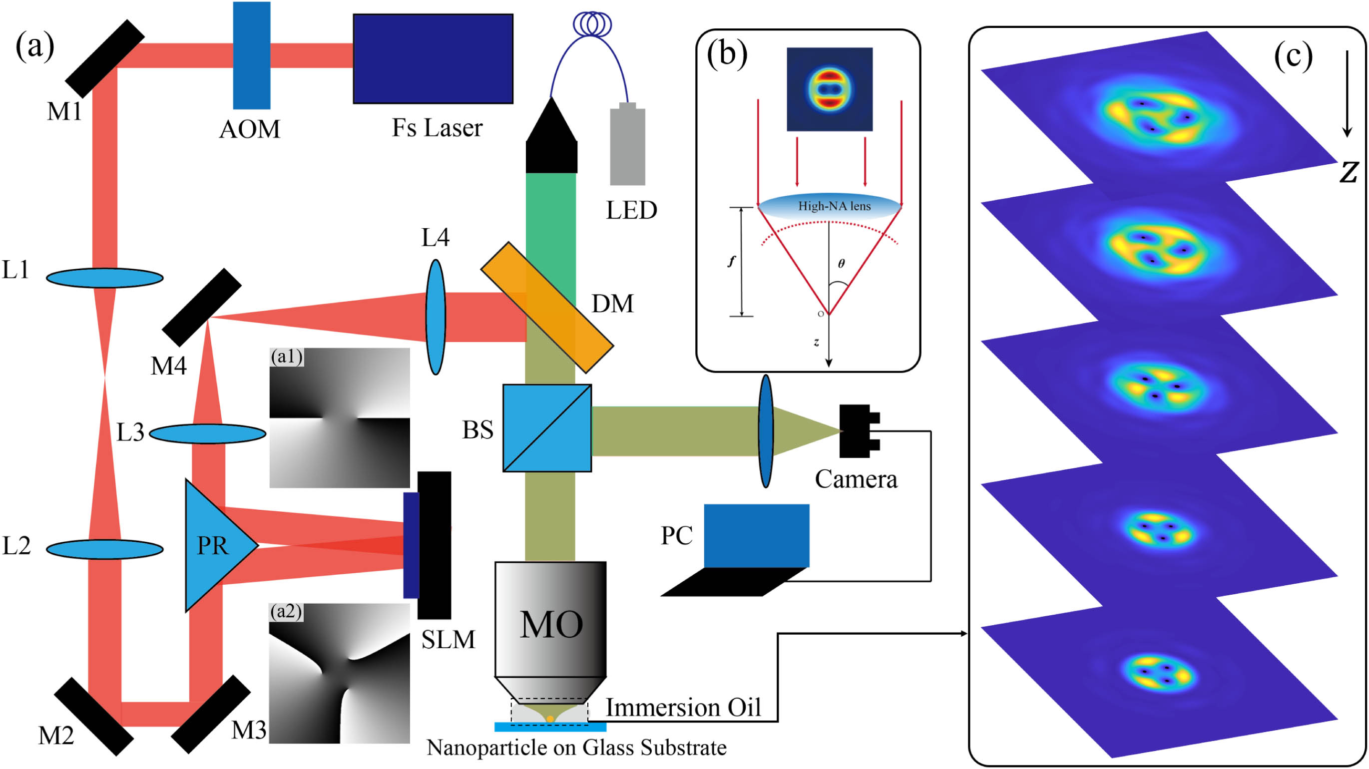
Figure 1.(a) Scheme of the experimental setup. The MVB is formed by applying phase-only modulation to a Gaussian beam. The initial phase distribution loaded on SLM is demonstrated here with , (a1) and (a2) as examples. Then, the generated MVB is coupled into a high NA immersion-type objective (MO) and focused onto the sample, consisting of a particle sitting on a glass substrate. The sample is embedded in immersion oil index matched to the substrate. The backward-scattered and reflected light is imaged with a camera. This is also the experimental setup for 2PP-DLW by MVBs. AOM, acousto-optic modulator; M, mirror; HWP, half-wave plate; PBS, polarized beam splitter; L, lens; PR, prism reflector; SLM, spatial light modulator; DM, dichroic mirror; BS, beam splitter. (b) Tight focusing system. (c) Simulated intensity distributions along the propagation direction in the focus region of an objective with NA of 1.45.
Figure 2.(a1)–(a4) Theoretical and (b1)–(b4) experimental intensity distributions of the MVBs at the focal plane () with an oil immersion objective (, ) and (a1), (b1) , ; (a2), (b2) , ; (a3), (b3) , ; (a4), (b4) , . Scale bar: 100 nm.
For visualization of the vortex line evolution at the nanoscale and fabrication of nanostructures based on 2PP-DLW, the MVBs need to be tightly focused by a high NA objective. Thus, the analysis of the tight focusing properties is critical. First of all, for simplifying the analysis of the MVBs, the time domain of the femtosecond pulsed beam is ignored. The tightly focusing system is shown in Fig. 1(b).
Given the vectorial nature of the MVBs, in this section, the Richards–Wolf diffraction theory is utilized to describe the tight focusing phenomenon of a high NA objective by calculating the three orthogonal field components , , and . According to the Richards–Wolf vectorial diffraction integration, the tightly focused field can be calculated by where are the coordinates of the output plane, is the focal length, and is the polar angle of the output pupil (). For the incident plane, and . is apodization function (for an aplanatic lens, ) and is the polarization vector, which is set as
To measure the deformation of the focal spot and reconstruct the focal field distribution, we use a scanning technique in which a gold nanosphere sitting on a glass substrate is utilized as a field probe [40]. The gold nanosphere is scanned through the focal plane by a 3D piezo stage. The objective collects the scattered and reflected light. For each position of the particle relative to the beam, the corresponding image is recorded with a camera. The measured data is utilized to directly showcase the deformation of the focal spot. The experimental setup is shown in Fig. 1(a). Suitable phase masks as shown in Figs. 1(a1) and 1(a2) for creating MVBs are produced using a computer-generated holography (CGH) technique and sent to an SLM. The SLM used in the experiment is a reflection-type phase-modulation SLM (SLM, LCOS-SLM, Hamamatsu, Japan) with , 12.5 μm pixel pitch. The active area is . The SLM is illuminated by a femtosecond laser with a center wavelength of 780 nm to produce the desired MVBs. The femtosecond laser source is a Ti:sapphire laser with dispersion precompensation (Chameleon Vision II, Coherent Inc., USA). The pulse duration time and repetition rate of the laser are 140 fs and 80 MHz, respectively.
Combining with Eqs. (1) and (3), the numerical integration allows us to visualize the tight focusing characteristics of the light field generated by MVBs. Figure 2 shows the theoretical and experimental intensity distributions of the MVBs with the indicated topological charge and initial off-axis distance at the focal plane with and . Comparing the initial phase distribution in Figs. 1(a1) and 1(a2) with the intensity distribution in Figs. 2(a1) and 2(a3), respectively, an intriguing phenomenon can be found whereby the two vortices of the incident beam locate in the horizontal direction while they locate in the vertical direction in the focal plane. During the tight focusing process by high NA objective, the phase vortices move towards each other when approaching the focal plane and rotate up to [33] in the focal plane due to Gouy phase shift [32].
Figure 3.(a) Visualization of numerically determined 3D evolution of phase vortices. The intensity distribution at the focal plane is also shown. The red dots here represent the vortices. (b) Top view of (a). (c) Numerical results for the evolution of MVBs at different propagation distance with and in the tight focusing system as shown in Fig. 1(b). Vortices are marked white dots with the indication of corresponding indices. (d) SEM photo of nanostructure of positive photoresist fabricated by single exposure 2PP-DLW recording the evolution of the phase vortices.
3. VORTEX EVOLUTION RECORDED BY POSITIVE PHOTORESIST
Phase singularities were first recognized as a general phenomenon of wave phase in a seminal paper by Nye and Berry [1]. Optical phase singularities have been a fashionable topic in optical physics for a long time, partly through their relationship with beams carrying orbital angular momentum [2], and a range of techniques have been developed to generate optical fields containing vortices [41]. The evolution of phase vortices where the intensity of the field is equal to zero during tight focusing is an intriguing phenomenon. We experimentally investigate the evolution of the phase vortices along the direction by patterning the light field in positive photoresist based on 2PP-DLW. The positive photoresist is a type of photoresist in which the portion of the photoresist exposed to light becomes soluble to the photoresist developer [30]. Thus, this kind of photoresist is utilized to record the vortex line evolution and investigate the propagation properties. The 2PP-DLW system in the experiment is schematically shown in Fig. 1(a), which is the same as the gold scanning experimental setup. The simulation and experimental results are shown in Fig. 3.
The numerically determined propagation dynamics of phase vortices are additionally illustrated in Fig. 3(a). Figure 3(b) shows the top view of Fig. 3(a). The phase vortices rotate during tight focusing. It can also be understood by Fig. 3(c) that the positions of the phase vortices denoted by white dots vary with the propagation distance . To directly demonstrate the evolution of phase singularities, the positive photoresist is employed here to record the 3D vortex line evolution of MVBs in the tight focusing system. Scanning electron microscopy (SEM) is tilted by 30° to show the 3D nanostructures fabricated by a positive photoresist. This nanostructure visualizes the 3D evolution of the vortex line in the space. The inset of Fig. 3(b) is the top view of Fig. 3(d), which is in good agreement with the theoretical results of the vortex line in Fig. 3(b). Despite the existence of aberration in the tightly focusing system, the evolution of phase singularities shown in SEM photos by single exposure on positive photoresist by 2PP-DLW is highly consistent with the numerical results in Fig. 3(b). Thus, it is straightforward to illustrate the 3D vortex line evolution by utilizing positive photoresist-based 2PP-DLW.
Furthermore, we also investigate the evolution of the phase vortices of MVB with , as shown in Fig. 4. Figure 4(a) shows the numerical calculation results of the 3D evolution of phase vortices. The single exposure results on positive photoresist are exhibited in Fig. 4(b). The nanostructure fabricated by positive photoresist is also identical to the theoretical results in Fig. 4.
Figure 4.(a) Numerically calculated results of the evolution of phase vortices with and . The vortices are marked red dots. (b) The 2PP-DLW single-exposure results are observed by SEM.
4. FABRICATION OF CHIRAL 3D NANOSTRUCTURE BASED ON 2PP-DLW
As mentioned in Section 2, the phase vortices rotate during the tight focusing process, forming the shaped 3D light field. Thus, in this section, negative photoresist is utilized to record the intensity evolution based on 2PP-DLW. In the 2PP-DLW experiment, the MVBs are projected into a photoresist sample and complex 3D structures can be fabricated by a single exposure instead of point-to-point scanning. Figures 5(a1), 5(b1), and 5(c1) show the theoretical results of 3D intensity distributions of the MVBs with indicated parameters. The chiral nanostructures and the corresponding arrays fabricated by MVBs are imaged by SEM as shown in Figs. 5(a2), 5(a3), 5(b2), 5(b3), 5(c2), and 5(c3). The single exposure time () is 200 ms and the laser power () is 10.7 mW. The chiral nanostructures recorded by the photoresist are consistent with the intensity profiles in the plane. The diameter () of the nanostructure is relative to the topological charge . μ with , μ with , and μ with . The diameters of the fabricated structures increase with the increase of . Furthermore, the subunit of the nanostructure rotates near the focal plane. The rotation angle is defined as . The measured rotation angle is equal to 180°, 118°, and 75° with , 3, and 5, respectively. The rotation angle is proportional to . Therefore, the number of the subunits of the nanostructure and the rotation angle are both dependent on . The increase of the diameter, number of subunits, and rotation angle match the theoretical results.
Figure 5.Propagation evolution and 3D intensity distributions of MVBs with and (a1) , (b1) , (c1) . SEM photos of the fabricated 3D chiral nanostructures and the corresponding arrays via tightly focused MVBs with and (a2), (a3) ; (b2), (b3) ; (c2), (c3) .
Figure 6 shows the effect of the laser power and single exposure time on the diameters of the fabricated structures. The detailed information on the diameter is demonstrated in Fig. 6(b). The diameters increase with the increase of and , respectively, but are not in a linear relationship. It is demonstrated in Refs. [18,42,43] that has a relationship as and , where is the threshold laser power of 2PP-DLW and is the threshold single exposure time of 2PP-DLW. It can be explained by the nonlinear process of two-photon polymerization.
Figure 6.(a) SEM photos of the fabricated 3D chiral nanostructures with different laser power and single exposure time. (b) Dependence of the diameters of the fabricated nanostructures on the laser power and exposure time.
The optical response is a significant property for 3D nanostructures. The optical response can be effectively enhanced by 3D nanostructures, which have been applied in various applications including broadband circular polarizers and near-infrared optical rotation devices [44,45]. It is obviously observed in Fig. 5 that the fabricated nanostructures have chiral spatial morphologies, which absolutely cause a strong optical response to OAM. The nanostructures exhibit different optical responses to incident light with opposite OAM. Here, the vortex dichroism is adopted to show such optical response, which is defined as [24] where and are the reflection intensity of chiral nanostructures under the topological charge of and . In the detection process, the vortex beams with a constant wavelength of 532 nm and a defined topological charge interact with the chiral nanostructure, causing the change of the discrete OAM spectrum and the generation of VD.
The measurement process of VD is shown in Fig. 7(a). The phase-only SLM is utilized here to modulate the incident continuous beam into a vortex beam. The vortex beam is tightly focused by the objective onto to the nanostructure and then the reflected light is collected by CCD. The measured VD spectrum of the nanostructure [SEM photo is exhibited in Fig. 8(b)] with μ and the glass substrate is shown in Fig. 8(a). The chiral nanostructure is fabricated by the MVB with , , the laser power is 40 mW, and the single exposure time is 200 ms. The finite difference time domain (FDTD) method is employed to simulate the light intensity distributions passing through the nanostructure. The results are shown in Figs. 7(b1) and 7(c1). The excitation incident vortex beam is with . Figures 7(b2) and 7(c2) exhibit the experimental results, which are highly consistent with the simulation. Obviously, the intensity profile with is stronger than that with . Thus, the optical vortex dichroism varies with topological charge.
Figure 7.Principle of measuring vortex dichroism spectra. (a) Experimental setup for measuring VD. The phase-only SLM is used to imprint the vortex phase onto a Gaussian incident continuous beam. Then the vortex beam is tightly focused on the chiral nanostructure through the objective, and the reflected light is collected by CCD. The simulation and experimental results of intensity distributions passing through the nanostructures with (b1), (b2) and (c1), (c2) are demonstrated, respectively.
Figure 8.(a) Optical vortical dichroism measurements of the chiral nanostructure versus topological charge . The insert is the SEM photo of the measured nanostructure with μ. (b) SEM photo of the nanostructure with different chiral properties in the inner area and outer area.
By scanning the topological charges of the incident vortex beam from to , the VD versus on the nanostructure is demonstrated in Fig. 8(a). The error of the signal is caused by factors such as uneven energy distributions of the excitation vortex beam, imperfect structural space symmetry, system aberration, system vibration, and shift. Nevertheless, the experimental results still well demonstrate the chiral nanostructure responses to the spiral phase. It can be seen that the VD peak occurs at the topological charge of 10. The magnitude of VD can approach approximately 42%. When , the magnitude of VD is negative, which means the total intensity of the vortex excitation beam with a positive topological charge is weaker than that with a negative one. This strange phenomenon results from the different chiral properties with various parts of the nanostructure. The chiral nanostructure can be divided into two parts, named inner and outer area, as shown in Fig. 8(b). The vortex beam spot generally increases with the increase of topological charge. Thus, the excitation vortex beams mainly pass through the inner area of the nanostructure. With the increase of , the excitation vortex beam and the nanostructure interact in the outer area. Then, the VD reaches the peak when the incident vortex beam has a topological charge near 10, which is affected by experimental errors. Finally, when the vortex beam focal spot is larger than the nanostructure, i.e., there is no interaction between the vortex beam and chiral nanostructure, the VD is therefore almost equal to zero.
After modulation by the fabricated nanostructure, it is necessary to analyze the optical properties of the reflected vortex beam. Thus, we intend to discuss the significant OAM spectrum of the modulated beam. The discrete OAM spectrum is employed here. The complex amplitude of the reflected beam can be expanded into an angular-harmonic series [46]:
The complex amplitude of each angular harmonic is given by where represents the weight of each angular harmonic and is an integer. The incident beam is a pure OAM beam with a definite topological charge and a perfect ring-like intensity profile. After interacting with the chiral nanostructure, the reflected beam retains the topological properties well. The discrete numerically calculated OAM spectrum is shown in Fig. 9. The reflected mode is in the superposition states of multiple eigenstates, but the weight of the incident mode is always higher than 0.8 [see in Figs. 9(a) and 9(b), or Figs. 9(c) and 9(d)]. Furthermore, the OAM spectrum of the reflected beams with opposite incident modes is not symmetrical, caused by the VD phenomenon.
Figure 9.OAM spectrum analysis of the reflected OAM beams with different incident topological charges: (a) ; (b) ; (c) ; (d) . The insert figures are the respective phase distributions.
In summary, we both theoretically and experimentally investigate the tightly focused light field of multi-vortex beams with various topological charges and off-axis distances. Due to Gouy phase shift, the vortices in the light field of MVBs move towards each other to the focal plane and rotate during the focusing process. The positive photoresist combined with single exposure based on 2PP-DLW is utilized to visualize the propagation dynamics of phase vortices at the nanoscale. The experimental results are highly consistent with the theoretical simulations. It is a new and efficient method to reveal the vortex line evolution at the nanoscale. According to the intriguing rotation properties of the phase vortices, to form the shaped 3D light fields, we employ the MVBs to efficiently fabricate 3D chiral nanostructures. The nanostructures and their arrays are manufactured by a single exposure on negative photoresist via 2PP-DLW. The dependence of the diameters of the fabricated structures on the laser power and single exposure time, and the rotation angle on the topological charge, are additionally demonstrated. Furthermore, the fabricated 3D chiral nanostructures exhibit strong vortex dichroism when excited by the vortex beams carrying OAM. The optical vortex dichroism is therefore measured. The fabrication strategy proposed in this paper can efficiently obtain 3D chiral nanostructures with a high throughput. This method can also be generalized to exploit more complex optical beams, for example, beams with specific polarization singularities. It may have wide applications in the fields of optical sensing, advanced functional devices, and so on.
Acknowledgment
Acknowledgment. The authors acknowledge constructive discussions from Dr. Shangting You and Dr. Xi Liu on result analysis.
 AI Video Guide
  AI Picture Guide
 AI One Sentence