• Photonics Research
  • Vol. 9, Issue 3, 395 (2021)
Haofei Xu1, Zhimin Zhu2, Jiancai Xue1, Qiuqiang Zhan2, Zhangkai Zhou1、3、*, and Xuehua Wang1、4、*
Author Affiliations
  • 1State Key Laboratory of Optoelectronic Materials and Technologies, School of Physics, Sun Yat-sen University, Guangzhou 510275, China
  • 2Centre for Optical and Electromagnetic Research, South China Academy of Advanced Optoelectronics, South China Normal University, Guangzhou 510006, China
  • 3e-mail: zhouzhk@mail.sysu.edu.cn
  • 4e-mail: wangxueh@mail.sysu.edu.cn
  • show less
    DOI: 10.1364/PRJ.414047 Cite this Article Set citation alerts
    Haofei Xu, Zhimin Zhu, Jiancai Xue, Qiuqiang Zhan, Zhangkai Zhou, Xuehua Wang. Giant enhancements of high-order upconversion luminescence enabled by multiresonant hyperbolic metamaterials[J]. Photonics Research, 2021, 9(3): 395 Copy Citation Text show less
    Novel properties of AHMM. (a) Schematic configuration of a nanopatterned Au−Al2O3 multilayer HMM with emitters inside the gaps. Multilayers consist of Au−Al2O3 stacks with a thickness period of 10 nm and 20 nm, and four periods in total. Whole structure dispersion relationship is shown in the above illustration. (b) Hyperbolic region of the AHMM. Alternative metal and dielectric, with thickness far smaller than the wavelength, are used to form the structure. Effective parallel (ε‖) and perpendicular permittivity (ε⊥) are given by the two formulas inserted. When they are with the opposite sign, the dispersion of the body structure transforms from elliptical to hyperbolic (blue area). εm and εd represent the dielectric constant of the metal and the medium, respectively, and ρ is the filling ratio of the metal. (c) Purcell factor calculation for a dipole placed in the AHMM gaps (red line) and near the uniform HMM (blue line). High intensity of Purcell factor and multiwavelength-enhanced modes are revealed in the AHMM situation. (d) Normalized dissipated power spectra for a perpendicular dipole at a distance of h=10 nm above a uniform Au−Al2O3 multilayer HMM. The color scales indicate normalized dissipated power intensity (on a logarithmic scale).
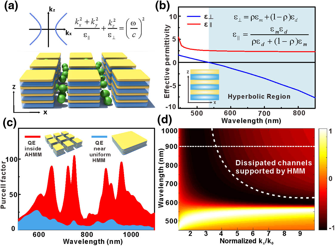
    Fig. 1. Novel properties of AHMM. (a) Schematic configuration of a nanopatterned AuAl2O3 multilayer HMM with emitters inside the gaps. Multilayers consist of AuAl2O3 stacks with a thickness period of 10 nm and 20 nm, and four periods in total. Whole structure dispersion relationship is shown in the above illustration. (b) Hyperbolic region of the AHMM. Alternative metal and dielectric, with thickness far smaller than the wavelength, are used to form the structure. Effective parallel (ε) and perpendicular permittivity (ε) are given by the two formulas inserted. When they are with the opposite sign, the dispersion of the body structure transforms from elliptical to hyperbolic (blue area). εm and εd represent the dielectric constant of the metal and the medium, respectively, and ρ is the filling ratio of the metal. (c) Purcell factor calculation for a dipole placed in the AHMM gaps (red line) and near the uniform HMM (blue line). High intensity of Purcell factor and multiwavelength-enhanced modes are revealed in the AHMM situation. (d) Normalized dissipated power spectra for a perpendicular dipole at a distance of h=10  nm above a uniform AuAl2O3 multilayer HMM. The color scales indicate normalized dissipated power intensity (on a logarithmic scale).
    Electric field distribution of AHMM. (a) Electric field distribution of the AHMM in XY and XZ planes within two cells inspired by plane wave in hyperbolic region (at 980 nm). Extensive EF hot spots are spread over the gap homogeneously. The array is with period of 220 nm and side length of 130 nm (i.e., gap distance of 90 nm). (b) Electric field distribution of the AHMM in XY and XZ planes with smaller gap (40 nm). A stronger and more homogeneous field distribution is formed as the gap becomes smaller. (c) Electric field distribution of the pure Au pillar array with the same size as in (b) XY and XZ planes (resonance 830 nm). (d) Gradient of electric field intensity from (a) in XY plane. Four gradients of XY plane are calculated with different Z values (position “Z=0” is marked in (a) with gray solid line).
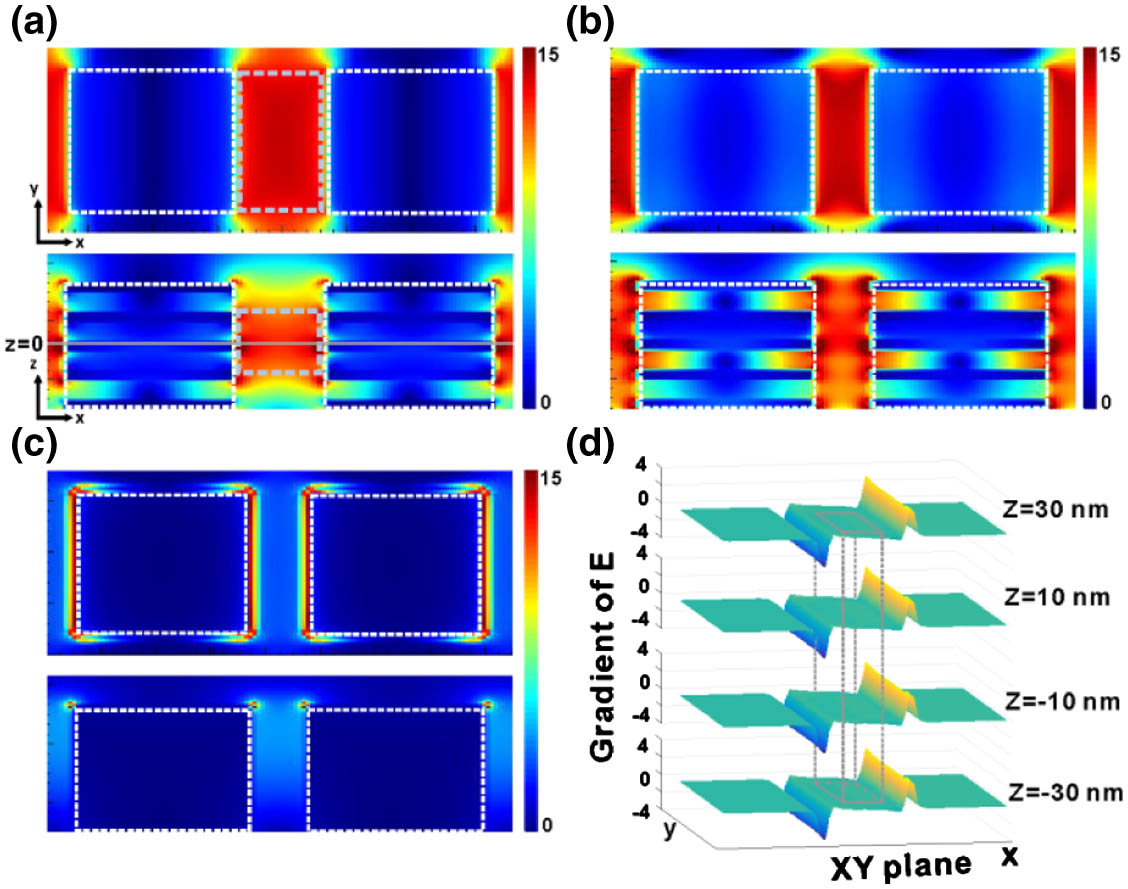
    Fig. 2. Electric field distribution of AHMM. (a) Electric field distribution of the AHMM in XY and XZ planes within two cells inspired by plane wave in hyperbolic region (at 980 nm). Extensive EF hot spots are spread over the gap homogeneously. The array is with period of 220 nm and side length of 130 nm (i.e., gap distance of 90 nm). (b) Electric field distribution of the AHMM in XY and XZ planes with smaller gap (40 nm). A stronger and more homogeneous field distribution is formed as the gap becomes smaller. (c) Electric field distribution of the pure Au pillar array with the same size as in (b) XY and XZ planes (resonance 830 nm). (d) Gradient of electric field intensity from (a) in XY plane. Four gradients of XY plane are calculated with different Z values (position “Z=0” is marked in (a) with gray solid line).
    Theoretical calculation of Purcell factor with different AHMM parameters. (a) Schematic of the AHMM structure in XY view. Dipole is placed at the center inside the gap, and the polarization is parallel to the X axis. Side a1 and a2 represent being parallel and perpendicular to the polarization direction of the dipole. (b) Purcell factor of the dipole with a1=a2 =130 nm, d=90 nm. Three obvious peaks, which correspond to the HMM modes, at 650 nm, 745 nm, and 980 nm are labeled in the order 1, 2, 3, respectively. (c) and (d) Distribution of three modes varies with side length of cell: (c) changing the side length of a1; (d) changing the side length of a2. There are individually adjustable modes by introducing pattern. (e) and (f) Distribution of three modes changes with HMM constituent: (e) changing the permittivity of dielectric; (f) changing the metal filling ratio. As the nature of the AHMM structure changes, all three modes move subsequently.
    Fig. 3. Theoretical calculation of Purcell factor with different AHMM parameters. (a) Schematic of the AHMM structure in XY view. Dipole is placed at the center inside the gap, and the polarization is parallel to the X axis. Side a1 and a2 represent being parallel and perpendicular to the polarization direction of the dipole. (b) Purcell factor of the dipole with a1=a2=130  nm, d=90  nm. Three obvious peaks, which correspond to the HMM modes, at 650 nm, 745 nm, and 980 nm are labeled in the order 1, 2, 3, respectively. (c) and (d) Distribution of three modes varies with side length of cell: (c) changing the side length of a1; (d) changing the side length of a2. There are individually adjustable modes by introducing pattern. (e) and (f) Distribution of three modes changes with HMM constituent: (e) changing the permittivity of dielectric; (f) changing the metal filling ratio. As the nature of the AHMM structure changes, all three modes move subsequently.
    Theoretical calculation of Purcell factor with different dipole positions. (a) Schematic of the AHMM in XZ view. Three representative positions of dipole are marked in the picture. (b) Purcell factor of dipole at different positions that correspond with (a). More enhanced modes can be found only when emitter is placed inside the gap of AHMM. (c) Spatial mapping of Purcell factor enhancement around the cell at three different wavelengths of the modes. Polarization of the used dipole is parallel to the X direction.
    Fig. 4. Theoretical calculation of Purcell factor with different dipole positions. (a) Schematic of the AHMM in XZ view. Three representative positions of dipole are marked in the picture. (b) Purcell factor of dipole at different positions that correspond with (a). More enhanced modes can be found only when emitter is placed inside the gap of AHMM. (c) Spatial mapping of Purcell factor enhancement around the cell at three different wavelengths of the modes. Polarization of the used dipole is parallel to the X direction.
    Preparation and characterization of samples. (a) Schematic of the fabrication process with electron beam evaporation and focused ion beam technology. (b) SEM image of AHMM structure at different magnification. Eight alternative layers can be seen clearly from insert. Roughness in the edge of array is mainly caused by the deposition and milling technology conducted at the subhundred nanometer scale. (c) Statistics of nanoparticle counts on silicon substrate and AHMM with different concentrations. (d) Optical microscope photograph including the AHMM with an excitation laser spot under 100× objective lens. (e) SEM image of UCNPs on (i) AHMM and (ii) silicon substrate with concentration C0 (12.5 mmol/L) and 10%C0, respectively. The area of view field is approximately the same as the laser spot in (d).
    Fig. 5. Preparation and characterization of samples. (a) Schematic of the fabrication process with electron beam evaporation and focused ion beam technology. (b) SEM image of AHMM structure at different magnification. Eight alternative layers can be seen clearly from insert. Roughness in the edge of array is mainly caused by the deposition and milling technology conducted at the subhundred nanometer scale. (c) Statistics of nanoparticle counts on silicon substrate and AHMM with different concentrations. (d) Optical microscope photograph including the AHMM with an excitation laser spot under 100× objective lens. (e) SEM image of UCNPs on (i) AHMM and (ii) silicon substrate with concentration C0 (12.5 mmol/L) and 10%C0, respectively. The area of view field is approximately the same as the laser spot in (d).
    Experimental emission measurements for UCNPs on different samples. (a) Upconversion mechanism in Yb3+/Tm3+ co-doped UCNPs under 980-nm excitation. (b) Design idea of AHMM. Blue solid line is the absorption spectrum of UCNPs, and red solid line is the Purcell factor of a dipole in AHMM. Peaks of Purcell factor are designed to match the excitation and emission wavelengths of the three- and four-photon processes. (c) Spectra of UCNPs on AHMM structure. Excitation power varies from 0.05 mW to 10.0 mW. (d) Excitation power dependence of UCNPs’ emission intensity presented in logarithm scale. Top left, UCNPs on AHMM; bottom right: UCNPs on Si substrate. (e) Enhancement factor of the upconversion processes. Descent occurs at 6.0 mW because the UCNPs on AHMM enter the supersaturation stage, while the UCNPs on Si substrate remain in the saturation region. (f) Emission ratios of 650 nm (triangle) and 745 nm (circle) to 800 nm on silicon substrate (blue line) and AHMM structure (red line). Ratios remain basically unchanged on the blank substrate and improve significantly in the AHMM structure as the power increases.
    Fig. 6. Experimental emission measurements for UCNPs on different samples. (a) Upconversion mechanism in Yb3+/Tm3+ co-doped UCNPs under 980-nm excitation. (b) Design idea of AHMM. Blue solid line is the absorption spectrum of UCNPs, and red solid line is the Purcell factor of a dipole in AHMM. Peaks of Purcell factor are designed to match the excitation and emission wavelengths of the three- and four-photon processes. (c) Spectra of UCNPs on AHMM structure. Excitation power varies from 0.05 mW to 10.0 mW. (d) Excitation power dependence of UCNPs’ emission intensity presented in logarithm scale. Top left, UCNPs on AHMM; bottom right: UCNPs on Si substrate. (e) Enhancement factor of the upconversion processes. Descent occurs at 6.0 mW because the UCNPs on AHMM enter the supersaturation stage, while the UCNPs on Si substrate remain in the saturation region. (f) Emission ratios of 650 nm (triangle) and 745 nm (circle) to 800 nm on silicon substrate (blue line) and AHMM structure (red line). Ratios remain basically unchanged on the blank substrate and improve significantly in the AHMM structure as the power increases.
    Haofei Xu, Zhimin Zhu, Jiancai Xue, Qiuqiang Zhan, Zhangkai Zhou, Xuehua Wang. Giant enhancements of high-order upconversion luminescence enabled by multiresonant hyperbolic metamaterials[J]. Photonics Research, 2021, 9(3): 395
    Download Citation