1State Key Laboratory of Optoelectronic Materials and Technologies, School of Physics, Sun Yat-sen University, Guangzhou 510275, China
2Centre for Optical and Electromagnetic Research, South China Academy of Advanced Optoelectronics, South China Normal University, Guangzhou 510006, China
Photonic nanostructures with resonant modes that can generate large electric field (EF) enhancements are applied to enhance light-matter interactions in nanoscale, bringing about great advances in both fundamental and applied science. However, a small hot spot (i.e., the regions with strong EF enhancements) and highly inhomogeneous EF distribution of the resonant modes usually hinder the enhancements of light-matter interactions in a large spatial scale. Additionally, it is a severe challenge to simultaneously generate multiple resonant modes with strong EF enhancements in a broadband spectral range, which greatly limits the capacity of a photonic nanostructure in boosting optical responses including nonlinear conversion, photoluminescence, etc. In order to overcome these challenges, we presented an arrayed hyperbolic metamaterial (AHMM). This AHMM structure is applied to simultaneously enhance the three-photon and four-photon luminescence of upconversion nanoparticles. Excitingly, the enhancement of the three-photon process is 1 order of magnitude larger than previous records, and for the enhancing four-photon process, we achieve an enhancement of 3350 times, greatly beneficial for overcoming the crucial problem of low efficiency in near infrared light upconversion. Our results demonstrated a promising platform for realizing giant enhancements of light-matter interactions, holding potential in constructing various photonics applications such as the nonlinear light sources.
1. INTRODUCTION
Boosting light-matter interactions in nanoscale by using photonic nanostructures lies at the heart of photonics-based science and technology, because related studies can not only enrich our basic understandings by discovering novel phenomena (such as room-temperature strong coupling at quantum limit, spaser, and giant nonlinear response) [1–3] but also have brought about advanced applications [4,5]. To enhance light-matter interactions, a large variety of photonic platforms, such as photonic crystals, dielectric microcavities, and plasmonic resonators, have been developed throughout the last decades [6,7], creating great value for various fields ranging from physics, chemistry, biology, and medicine to geology and art, cultivating fruitful applications like surface-enhanced Raman spectroscopy, photocatalysis, biosensors, and photothermal therapy [8–16].
Generally, the resonant modes of photonic structures can greatly enhance the electric field (EF) in hot spots (i.e., the regions with strong EF enhancements), and therefore they are extensively applied to enhance light-matter interactions [17]. Despite the remarkable advances made by the resonant modes, small hot spots and highly inhomogeneous EF distribution of the resonant modes greatly limit their capacity in enhancing light-matter interactions in a large scale. It is also difficult to simultaneously generate multiple resonant modes with strong EF enhancements in a broadband spectral range. This makes it very hard to realize strong optical enhancements simultaneously at the wavelengths of both pumping and radiation, and therefore limits the enhancement effects in various optical processes such as nonlinear conversion and photoluminescence [18–20]. To date, a photonic platform that can simultaneously address these problems is lacking.
To overcome the abovementioned challenges, we propose the arrayed hyperbolic metamaterials (AHMMs) consisting of two-dimensional periodic hyperbolic pillars. Hyperbolic metamaterials (HMMs) are famous for supporting the infinite photonic density of states (PDOS), large EF enhancements, and broadband electromagnetic manipulation [21,22], which enable the possibility of multiresonant modes in a broadband spectral range. Furthermore, due to the bulk material response [23], the hot spots of their resonant modes can be homogeneously distributed in the interstitial space of adjacent pillars. This also leads to a vast spatial overlapping inside the structure gaps, giving rise to the simultaneous functioning of these modes and benefiting multiwavelength applications. To demonstrate the promising potential of the AHMM, we applied the AHMM to enhance a high-order nonlinear response of rare-earth upconversion nanoparticles (UCNPs). The -photon upconversion emissions of rare-earth UCNPs, especially the high-order processes (i.e., ), offer a wide variety of applications including deep-tissue biophotonics, multioptical coding, and so on [24,25]. However, these high-order nonlinear processes are greatly suffering from their low intensities [26]. Herein, by using the AHMMs, we obtained giant enhancements of high-order nonlinear processes simultaneously (i.e., 1800 and 3350 times luminescence enhancements for three- and four-photon processes, respectively). These results validate the excellent performance of the AHMM in serving as a photonic platform for enhancing light-matter interactions, indicating promising potential in various applications, such as multiple frequency conversion, nanoscale lasers, and quantum information processing [27–30].
Sign up for Photonics Research TOC. Get the latest issue of Photonics Research delivered right to you!Sign up now
2. EXPERIMENT
A. Fabrication of the AHMM Structure
A clean silicon wafer was prepared as the primal substrate. Four pairs of Au and layers were alternatively deposited by using electron beam evaporation (Ohmiker-50B), with the thickness of Au and layers being and , respectively. The deposition rates of both materials were set to be 1.0 A/s, and the base pressure of the evaporation chamber was (1 Torr = 133.322 Pa). After that, nanopatterns were engraved into the uniform HMM by a focused ion beam system (AURIGA, ZEISS) to form the final structures. The dose of an ion beam was μ, and the beam current was 50 pA under 30 kV.
B. Synthesis of UCNPs
The designed UCNPs were synthesized following previously reported protocols with some modifications [31–33]. In this synthesis process, a (Ln = Y/Yb/Tm) stock solution (0.2 M, 1 M = 1 mol/L) was added into a 100 mL round bottom flask, followed by the addition of 7.5 mL oleic acid (OA) and 17.5 mL 1-octadecene (ODE). The mixture was heated to 150°C under stirring for 40 min to form the lanthanide-oleate precursor solution and then cooled down to room temperature. Then 10 mL of -methanol solution (0.4 M) and 2.5 mL of NaOH-methanol solution (1.0 M) were pipetted into a 15 mL centrifuge tube, and then the mixture solution was quickly injected into the flask. Subsequently, the mixture was heated to 50°C and kept at that temperature for at least 0.5 h. Then it was heated to 110°C under vacuum to remove methanol. After the methanol was evaporated, the mixture was heated to 300°C and incubated at that temperature for 1.5 h under an argon atmosphere, and then cooled down to room temperature. The UCNPs were precipitated by the addition of ethanol, followed by centrifugation at 7500 r/min for 5 min. The obtained UCNPs were washed several times using ethanol and cyclohexane and were finally redispersed into cyclohexane for subsequent use.
C. Optical Measurement
Photoluminescence (PL) spectra of the UCNPs were measured by a confocal microspectroscopic system. The pump laser, a continuous wavelength laser at 980 nm, was focused on the sample by a focusing lens (N.A. = 0.9) with a spot size of 3.8 μm in diameter. Then, the photoluminescence from samples was collected through the same focusing lens with a collecting angle of and a shortpass filter (900 nm) blocking the laser signal. Finally, a spectrometer (Princeton Instruments Acton SP2750) was applied to obtain the PL spectra.
D. Numerical Simulation
The simulation was performed using a commercial software, Lumerical FDTD Solutions. The refractive indexes of Au and were from the experimental data of CRC and Palik. The finest mesh size was set to be 0.5 nm inside and near the structure. A dipole source ranging from visible light to near infrared was used to get the Purcell factor () and external quantum efficiency (). The Purcell factor result is equivalent to dividing the power emitted by a dipole source in the environment by the power emitted by the dipole in a homogeneous environment (bulk material), since the emission rate is proportional to the local density of optical states (LDOS), and the LDOS is proportional to the power emitted by the source. The external quantum efficiency of a dipole source was defined as the division of radiative flux to the total photon flux. In FDTD Solutions, we could get the radiative flux by a large enough power monitor set in the far-field (more than a wavelength) and use the transmission box surrounding the dipole at the very near field scale (2 nm) to obtain the total photon flux. Then the value of was calculated by dividing them. The simulation time was set to 1000 fs to ensure the convergence of the results.
E. Theoretical Calculation for Normalized Dissipated Power Spectra
When a dipole emitter is placed at a distance of above the planar multilayer with the polarization perpendicular () or parallel () to the multilayer interface, the normalized dissipated power () of this dipole can be written as [34,35]where is the magnitude of the wavevector in a vacuum, is the wavevector component parallel to the multilayer surface normalized by the vacuum wavevector, is the component of the wavevector perpendicular to the multilayer interface, is the relative permittivity for the host material, and , are the reflection coefficient at the interfaces for a - or -polarized wave, respectively.
3. RESULT AND DISCUSSION
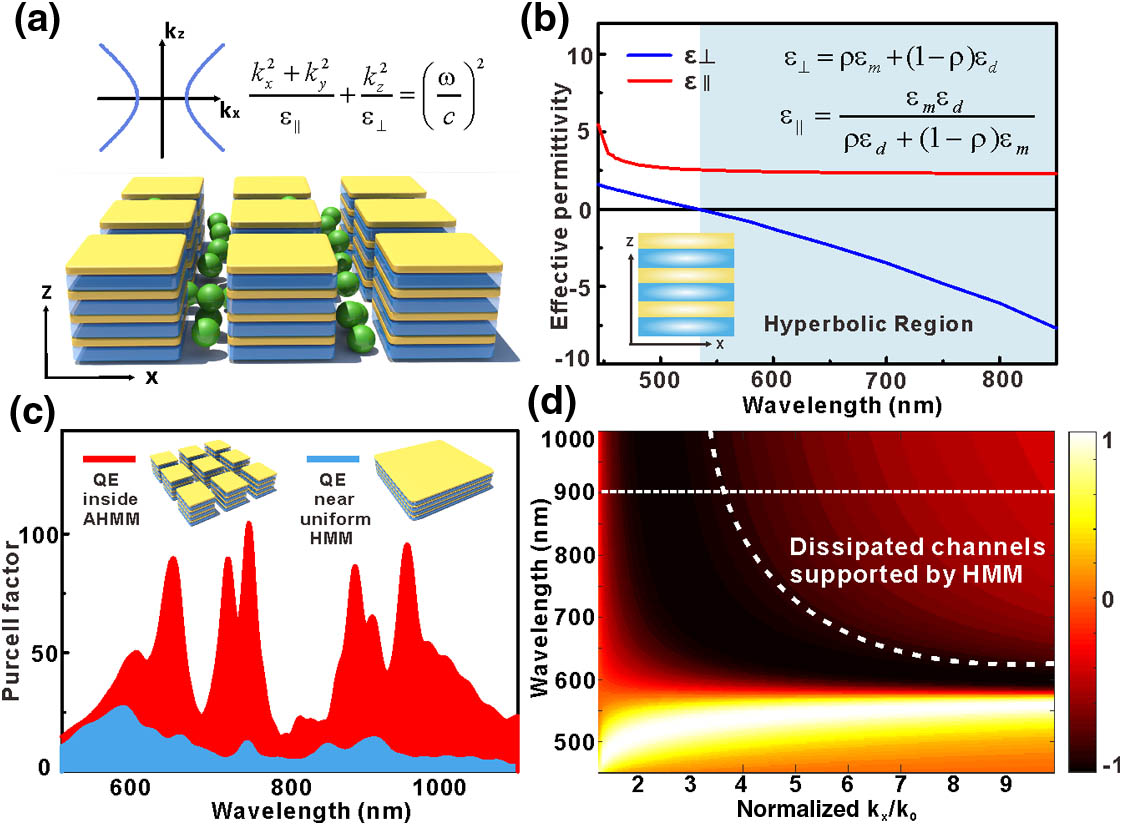
Figure 1.Novel properties of AHMM. (a) Schematic configuration of a nanopatterned multilayer HMM with emitters inside the gaps. Multilayers consist of stacks with a thickness period of 10 nm and 20 nm, and four periods in total. Whole structure dispersion relationship is shown in the above illustration. (b) Hyperbolic region of the AHMM. Alternative metal and dielectric, with thickness far smaller than the wavelength, are used to form the structure. Effective parallel () and perpendicular permittivity () are given by the two formulas inserted. When they are with the opposite sign, the dispersion of the body structure transforms from elliptical to hyperbolic (blue area). and represent the dielectric constant of the metal and the medium, respectively, and is the filling ratio of the metal. (c) Purcell factor calculation for a dipole placed in the AHMM gaps (red line) and near the uniform HMM (blue line). High intensity of Purcell factor and multiwavelength-enhanced modes are revealed in the AHMM situation. (d) Normalized dissipated power spectra for a perpendicular dipole at a distance of above a uniform multilayer HMM. The color scales indicate normalized dissipated power intensity (on a logarithmic scale).
With the consideration of our mature fabrication techniques, we set the thicknesses of Au and layers as 10 nm and 20 nm, respectively. Therefore, one can calculate that the hyperbolic region begins from 540 nm, where the AHMM shows much better performance in boosting light-matter interactions over uniform HMM. Similar to previous studies [36,37], the enhancement of the light-matter interaction discussed in this paper is also described by calculating the Purcell factor of a quantum emitter (QE, which is a dipole source) placed near our studied metamaterials [Fig. 1(c)]. In contrast with the results obtained by placing the QE near uniform HMM, the QE located in the gap of AHMM exhibits higher Purcell factors, and the value of the Purcell factors reaches multiple peaks under varied QE wavelengths. These peaks actually correspond to the resonant modes of HMM, which represent propagating modes within the HMM that result from hybridization of the individual surface plasmon polariton (SPP) modes associated with each metal-dielectric interface [38]. To further understand the broadband Purcell response, the normalized dissipated power spectra are calculated. Figure 1(d) shows the normalized dissipated power spectra for a perpendicular dipole placed 10 nm above the hyperbolic multilayer surface. The emission wavelength of this dipole varies from 450 nm to 1000 nm, and the calculation methods for the dissipated power with the varied wavelength are given in Section 2.E. The Purcell factor of a dipole can be calculated by integrating its dissipated power from 0 to wavevector [34,35]. For example, the Purcell factor of a dipole with an emission wavelength at 900 nm can be obtained by integrating the data marked by the white line in Fig. 1(d). As shown by Fig. 1(d), one can find that except for the spectral range around the instinct plasmon mode of Au at about 530 nm, the large dissipated power can also be found over a broadband spectral region in the high wavevector region (i.e., the top-right corner marked by a white-dashed line), which is a unique character for hyperbolic nanostructures [34]. Owing to the existence of this large dissipated power in the top-right corner, the hyperbolic multilayer can support large Purcell factors in a broadband spectral range. In short, the optical behavior of our AHMM can be attributed to the Bloch-like gap plasmon polaritons with high modal confinement inside the multilayer [37–39].
Figure 2.Electric field distribution of AHMM. (a) Electric field distribution of the AHMM in and planes within two cells inspired by plane wave in hyperbolic region (at 980 nm). Extensive EF hot spots are spread over the gap homogeneously. The array is with period of 220 nm and side length of 130 nm (i.e., gap distance of 90 nm). (b) Electric field distribution of the AHMM in and planes with smaller gap (40 nm). A stronger and more homogeneous field distribution is formed as the gap becomes smaller. (c) Electric field distribution of the pure Au pillar array with the same size as in (b) and planes (resonance 830 nm). (d) Gradient of electric field intensity from (a) in plane. Four gradients of plane are calculated with different values (position “” is marked in (a) with gray solid line).
Figure 3.Theoretical calculation of Purcell factor with different AHMM parameters. (a) Schematic of the AHMM structure in view. Dipole is placed at the center inside the gap, and the polarization is parallel to the axis. Side and represent being parallel and perpendicular to the polarization direction of the dipole. (b) Purcell factor of the dipole with , . Three obvious peaks, which correspond to the HMM modes, at 650 nm, 745 nm, and 980 nm are labeled in the order 1, 2, 3, respectively. (c) and (d) Distribution of three modes varies with side length of cell: (c) changing the side length of ; (d) changing the side length of . There are individually adjustable modes by introducing pattern. (e) and (f) Distribution of three modes changes with HMM constituent: (e) changing the permittivity of dielectric; (f) changing the metal filling ratio. As the nature of the AHMM structure changes, all three modes move subsequently.
Figure 4.Theoretical calculation of Purcell factor with different dipole positions. (a) Schematic of the AHMM in view. Three representative positions of dipole are marked in the picture. (b) Purcell factor of dipole at different positions that correspond with (a). More enhanced modes can be found only when emitter is placed inside the gap of AHMM. (c) Spatial mapping of Purcell factor enhancement around the cell at three different wavelengths of the modes. Polarization of the used dipole is parallel to the direction.
Figure 5.Preparation and characterization of samples. (a) Schematic of the fabrication process with electron beam evaporation and focused ion beam technology. (b) SEM image of AHMM structure at different magnification. Eight alternative layers can be seen clearly from insert. Roughness in the edge of array is mainly caused by the deposition and milling technology conducted at the subhundred nanometer scale. (c) Statistics of nanoparticle counts on silicon substrate and AHMM with different concentrations. (d) Optical microscope photograph including the AHMM with an excitation laser spot under objective lens. (e) SEM image of UCNPs on (i) AHMM and (ii) silicon substrate with concentration (12.5 mmol/L) and , respectively. The area of view field is approximately the same as the laser spot in (d).
Figure 6.Experimental emission measurements for UCNPs on different samples. (a) Upconversion mechanism in co-doped UCNPs under 980-nm excitation. (b) Design idea of AHMM. Blue solid line is the absorption spectrum of UCNPs, and red solid line is the Purcell factor of a dipole in AHMM. Peaks of Purcell factor are designed to match the excitation and emission wavelengths of the three- and four-photon processes. (c) Spectra of UCNPs on AHMM structure. Excitation power varies from 0.05 mW to 10.0 mW. (d) Excitation power dependence of UCNPs’ emission intensity presented in logarithm scale. Top left, UCNPs on AHMM; bottom right: UCNPs on Si substrate. (e) Enhancement factor of the upconversion processes. Descent occurs at 6.0 mW because the UCNPs on AHMM enter the supersaturation stage, while the UCNPs on Si substrate remain in the saturation region. (f) Emission ratios of 650 nm (triangle) and 745 nm (circle) to 800 nm on silicon substrate (blue line) and AHMM structure (red line). Ratios remain basically unchanged on the blank substrate and improve significantly in the AHMM structure as the power increases.
In order to strictly study the emission enhancing effect, we measured UCNPs with nearly the same particle number on the AHMM and Si substrate. Typical emission spectra of UCNPs on AHMM are presented in Fig. 6(c), where three emission peaks with , 650 nm, and 745 nm can be clearly observed. Through extracting the peak value with the corresponding power separately and taking them in logarithm, one can see that the slopes (, where and are the intensity of unconversion emission and excitation power, respectively) of the fitted curves are about 2, 3, and 4 when is below 0.15 mW (defined as region 1), presenting strong evidence for the two-, three-, and four-photon luminescence [Fig. 6(d)] [44]. Also, it is well-known that the upconversion luminescence of rare-earth UCNPs exhibits the phenomenon of saturated absorption, which has also been observed from Fig. 6(d). Since the number of ions in UCNPs that can be excited from the ground state is finite, when the exceeds a threshold, it is reasonable to find that almost all the ions have been pumped to the excited state. In such a case, the number of photons absorbed by UCNPs will be reduced. Thereby, the value will gradually decrease with the increasing of . In Fig. 6(d), except for region 1 when the UCNPs are unsaturated with excitation light, another two regions can be observed. For one region, the values are basically reduced to half of the original ones ( varying from 0.15 mW to 6 mW), suggesting that the UCNPs enter a saturated state (defined as region 2). For another, as the continues to increase (region 3, beyond 6 mW), the values of all the three curves further reduce until they are close to 0, indicating that the UCNPs have reached a supersaturated state, and the UCNPs no longer absorb more photons no matter how much the increases.
For the UCNPs on the Si substrate, the phenomenon of saturated absorption can also be noticed. When the excitation is lower than 1.4 mW, one can find the of two-photon upconversion (i.e., ) is 1.97. In this range, the intensity of three- and four-photon emissions is too weak to read, so their results are blank. With the increasing of , of two-photon upconversion decreases to 1.03, and we can observe the three- and four-photon emissions with measured of 1.46 and 1.9, respectively. Based on these results, one can conclude that the saturation threshold of UCNPs on the Si substrate is 1.4 mW, which is nearly 1 order of magnitude larger than that of UCNPs on AHMM. The huge decreasing of the saturation threshold caused by AHMM results because the AHMM can increase excitation efficiency by creating higher pumping photon flux to excite to the excite state [41]. Note that after our samples have experienced the PL measurements with increasing from low to high, its spectral intensity is reproducible under the same . This fact indicates that the applied excitation light has not damaged our samples.
Following the discussion of the saturation threshold changing caused by AHMM, we go further to investigate the emission intensity enhancements of UCNPs enabled by AHMM. The enhancement factor is defined as the ratio of emission peak value of UCNPs on AHMM to that of UCNPs on the Si substrate [Fig. 6(e)]. One can find that all the three multiphoton upconversion emissions have been enhanced by the AHMM. However, since the three- and four-photon processes (i.e., and 745 nm) have optical enhancement at both excitation and emission wavelengths, their enhancement factors are obviously larger than that of the two-photon process (i.e., ). The three-photon and four-photon processes achieved the highest enhancements of 1800 and 3350 times, respectively. Compared to previous studies, our enhancement result of the three-photon process in rare-earth UCNPs systems is 1 order of magnitude larger [48–51]. Furthermore, we obtained a record for the enhancement of the four-photon process (the related reports of four-photon process enhancement in rare-earth UCNPs systems are rare), providing an effective and inspired way for the future study of this field. In addition, one can see that the emission enhancement factors have a large decline when the is over 6.0 mW. The reason is that UCNPs on AHMM enter the supersaturation state under such high , and the values of their multiphoton processes become smaller than that of UCNPs on the Si substrate [see Fig. 6(d)]. Since the enhancement factors of three- and four-photon emissions are larger than that of two-photon upconversion, the luminous intensities of three- and four-photon emissions gradually increase to a level comparable to the two-photon process for the UCNPs on our AHMM. More digitally, we use the two ratios of and to describe this tendency. The different colors (red and blue) and symbols (circle and triangle) represent the ratios of three- and four-photon processes in the silicon substrate and AHMM in Fig. 6(f). It is intuitional that the blue line is always maintained at about 12%, while the red line increases from 14% to 50% as the power increases, indicating that our AHMM structure does help improve the efficiency of the high-order nonlinear process.
Sign up for Photonics Research TOC. Get the latest issue of Photonics Research delivered right to you!Sign up now
In order to more clearly reveal the emission enhancing origin in our AHMM system, the theoretical enhancement factors for the three- and four-photon emissions are theoretically analyzed. In our system, the emission enhancement () can be given by , where the and are the enhancement factors at excitation and emission wavelengths, respectively. In the nonlinear upconversion process, the follows the relationship of , where is the intensity of excitation light, is the EF enhancement, and equals the fitting slope of the emission intensity-excitation power dependence curve in a double logarithm (i.e., the parameter mentioned in this paper) [52,53]. On the other hand, the Purcell factor is proportional to the imaginary part of Green’s function in a medium [36], and it can be regarded as . Therefore, the can be given as , where and are the Purcell factors at the excitation and emission wavelengths, respectively. In addition, the absorption of AHMM should be considered. So, adding the external quantum efficiency (), we considered the theoretical in our system follows the relationship of . The values of are obtained by FDTD simulations, and detailed calculation methods are given in Section 2.D.
Based on our experimental results, the three- and four-photon processes actually occurred when the UCNPs are in the saturated region. According to their values, one can find that should be 1.5 and 2 for the three- and four-photon processes. Thus, taking the values of , , and at the required wavelengths [ at 650 nm and 745 nm are 4.8% and 1.3%, respectively; the values of are given in Fig. 6(d)], the for three- and four-photon emissions [i.e., and ] can be calculated as 2570 and 4580, respectively. These results are quite near the experimental results. Furthermore, we can compare the ratio of to from both the theoretical and the experimental aspects, and find the values are also quite similar (1.78 and 1.86, respectively). The good agreement of the theoretical and experimental results further confirms the correctness of our work. It is noticed that improving emission directivity can also enhance emission intensity. However, in our cases, we calculated the emission directivity of a point source (i.e., a dipole) placed on a Si substrate and the middle of AHMM, and find that over 92% power radiated from this dipole is confined in a radiation angle of 65° and 38°, respectively. Since the collecting angle of our optical measurement system is , it can be concluded that the improvement of emission directivity caused by AHMM only has limited contributions to the emission enhancement.
4. CONCLUSION
In summary, we demonstrated a novel AHMM structure with large and multiple resonant modes for boosting light-matter interactions. Besides, this AHMM structure not only enables homogeneous hot spots in the gap region but also makes the hot spots overlap well in space for different resonant modes. We applied the AHMM structure to simultaneously enhance the high-order nonlinear emissions of UCNPs. The enhancement of the three-photon process is 1 order of magnitude larger than previous records in the three-photon enhancement of rare-earth UCNPs, and we even achieve a 3350 times enhancement of four-photon emission. The reasons for these unprecedented results can be attributed to two advantages of our AHMM. First, the EF distributions of various hot spots in AHMM are homogeneous in the spatial area, providing an environment of strong EF enhancement covering the whole UCNP inside the AHMM. Second, the hot spots are extremely overlapped in space for resonant modes matching the excitation and emission wavelengths of the nonlinear optical process, ensuring the two resonant modes function simultaneously. Our findings demonstrated a promising platform for the giant enhancement of light-matter interaction, which has potential to construct a high-efficiency nonlinear light source and multiplex photonic devices, providing new thoughts in designing functional photonic nanostructures.
Acknowledgment
Acknowledgment. X.H.W. and Z.K.Z presented the concept, conceived the research outline, and supervised the project. H.F.X. performed the sample fabrications, characterizations, and optical measurements. Z.M.Z and Q.Q.Z. synthesized the UCNPs. H.F.X made the numerical simulations. H.F.X., Z.M.Z., Z.K.Z., J.C.X., and Q.Q.Z. analyzed the theoretical and experimental results. H.F.X., J.C.X., Z.K.Z., and X.H.W. co-wrote the paper with inputs from all the authors. All the authors discussed the results.