
Hailong Wang, Jialin Ma, Jianhua Zhao. Giant modulation of magnetism in (Ga,Mn)As ultrathin films via electric field[J]. Journal of Semiconductors, 2019, 40(9): 092501
- Journal of Semiconductors
- Vol. 40, Issue 9, 092501 (2019)
Abstract
1. Introduction
Attributed to its scaling down capability and potential advantage on significantly lowering the power consumption, electrical control of magnetism has been one of the hottest topics in the research of spintronics[
As one of the very first demonstrations, dilute magnetic semiconductors (DMS) have played a very critical role, due to their features of combining carrier-mediated ferromagnetism and relatively low carrier density together[
In principle, the main obstacles that restrict the electric-field effect on the magnetism in (Ga,Mn)As lie in two aspects: firstly, stronger ferromagnetism requires larger hole density, which will then decrease the penetration depth of the electric-field and limit the electric-field effect; secondly, thinning down the (Ga,Mn)As films to less than ~5 nm usually makes it insulating and even destroys its ferromagnetism. Correspondingly, two routes could be employed to partly figure out these problems: one is using advanced techniques that can apply larger electric-field than the upper limit of conventional gating method, which usually uses solid state dielectrics as the gate insulator and results in a highest breakdown strength of electric-field of ~ 1 V/nm[
In this work, by a special layer structure design which suppresses the hole depletion near the interface of (Ga,Mn)As and GaAs or (Al,Ga)As layers, we successfully grew ferromagnetic ultrathin (Ga,Mn)As films with thickness down to ~2 nm. Moreover, these samples maintain relatively high TC (~100 K) and metallic transport properties. Furthermore, by using ionic liquid as the gate dielectric, giant modulation of magnetism via electric-field in (Ga,Mn)As thin film was realized. As indicated by the transport measurements, the largest variation of TC exceeds 100 K, which is nearly 5-times larger than previous results. Our results provide a new pathway for the efficient electrical control of magnetism in (Ga,Mn)As.
2. Sample design and device fabrication
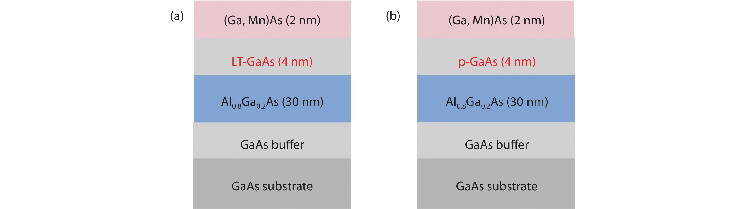
Two series of (Ga,Mn)As samples with thickness of ~2 nm were grown on GaAs (001) substrates by molecular-beam epitaxy (MBE), which are named as series-A and series-B samples, respectively. All the underlayers were deposited at ~560 °C, while the (Ga,Mn)As layer was grown at ~220 °C. In each set of samples, four (Ga,Mn)As samples with nominal Mn concentration of ~8%, 9%, 10% and 11% are prepared. The main difference between these two sets of samples is that the low-temperature grown GaAs or (Al,Ga)As underlayer in conventional layer structure were replaced by a heavily Be-doped GaAs layer. The layer structure is shown in Fig. 1, and the sample information is listed in Table 1. The doping concentration of the Be-doped GaAs is about 2 × 1019 cm–3, while its thickness is 4 nm, the same with the low-temperature GaAs layer. It is well known that the hole density in (Ga,Mn)As with TC higher than 100 K is usually in the range of 5 × 10¹⁹–2 × 1021 cm–3, which will be partly depleted at the interface, especially when the underlayer is low temperature grown n-type GaAs layer. This depletion phenomenon is not important when (Ga,Mn)As film is thick enough, but can be very crucial for ultrathin films, which might account for the insulating tendency of ultrathin (Ga,Mn)As films. Moreover, the hole-mediated ferromagnetism of (Ga,Mn)As will also be strongly weakened as a result of the hole depletion. For the above reasons, the heavily p-doped GaAs layers in series-B samples are expected to suppress the depletion of holes and the tendency of being insulating (or even loss of ferromagnetism) in (Ga,Mn)As ultrathin films.
![]()
Figure 1.(Color online) Schematic diagrams of the layer structure for (a) series-A and (b) series-B samples. The (Al,Ga)As buffer layer plays the role of an energy barrier, and the low-temperature grown n-type GaAs in series-A samples will deplete the holes in (Ga,Mn)As film to some extent, while the heavily-doped p-type GaAs layers in series-B samples are used to suppress the hole depletion.
Table Infomation Is Not EnableAfter being taken out from the MBE chamber, the (Ga,Mn)As samples were then annealed in the atmosphere at 220 °C for 1 h. Subsequently, 3-nm-thick HfO2 was deposited at 100 °C on (Ga,Mn)As by atomic layer deposition (ALD), during which the pulses of Hf(NMe2)4 and de-ionized water were alternatively generated with N2 purging between each period. The HfO2 can protect the ultrathin (Ga,Mn)As film from being damaged by the following device fabrication processes. The samples were then patterned into Hall-bar devices (10–30 μm wide) using photo-lithography and argon ion beam etching, following which an isolated Au/Cr electrode was formed by thermal evaporation and lift-off processes. Ionic liquid 1-ethyl-3-methyl imidazolium bis(trifluoromethylsulfonyl)imide (EMITFSI) was then dropped on the Hall device as the gate dielectric.
3. Magnetic and transport properties
Figs. 2(a) and 2(b) show the temperature dependent magnetization curves for these two series of heavily Mn-doped (Ga,Mn)As samples. A magnetic field of 20 Oe was applied along the GaAs [–110] direction, in order to cover the unknown influence of the residual magnetic field from the superconducting magnet in our magnetometer. As can be seen, all the samples exhibit well-defined ferromagnetism with their Curie temperatures ranging from around 80 to 135 K. It is clear that TC of both sets of samples increases with the increase of Mn content. However, no consistent enhancement of TC is observed for series-B samples, although they are expected to show stronger ferromagnetism due to the less depletion of holes near the interface. Notice that TC of sample B4 with 11% Mn content is higher than sample B3, but its magnetization at low temperature is smaller. The lower TC of sample B3 might be attributed to the strong compensation of holes by As antisites, while the lower magnetization for sample B4 can be ascribed to the antiferromagnetic Mn–Mn exchange interation (direct exchange without the assistance of holes).
![]()
Figure 2.(Color online) Temperature dependence of the magnetization for (a) series-A and (b) series-B samples. The magnetic field of 20 Oe is applied along the (Ga,Mn)As [–110] direction. An enhancement of
As for the transport properties, we mainly focus on the temperature dependence of longitudinal resistance (R–T curves). Figs. 3(a) and 4(b) plots the R–T curves for both series of samples, and the results are very different. For series-A samples, the sample resistances increase rapidly when decreasing the temperature and even become unmeasurable except sample A3 with 10% Mn content. On the contrast, the sample resistances of series-B samples increase first and then decrease with decreasing the temperature, similar with the typical behaviors of metallic thick (Ga,Mn)As films. In comparison with the transport results of series-A samples, we conclude that the heavily-doped p-GaAs underlayer does suppress the depletion of holes in (Ga,Mn)As to some extent, although it does not show observable influence on their magnetization data.
![]()
Figure 3.(Color online) (a) Longitudinal resistance as a function of temperature for series-A samples. (b) Temperature dependent longitudinal resistances of sample A4 under gate voltages, in which the peak shifts to lower (higher) temperature when the applied voltage is +2 V (–2 V).
![]()
Figure 4.(Color online) (a) Schematic of the device structure. (b) Longitudinal resistance as a function of temperature for series-B samples. (c, d) Temperature dependent longitudinal resistances for samples B4 and B1 under various gate voltages, in which clear peak shifts can be observed.
It is well established that the R–T curves of metallic (Ga,Mn)As sample can be used to estimate its TC, which is roughly corresponding to the metal-insulator transition temperature[
4. Giant electric-field effect on magnetism
The gate electric-field was applied between the isolated electrode and one of the current leads, as shown in Fig. 4(a). The R–T curve was then recorded with the gate voltage (VG) fixed at a certain value during the whole measurement process. Fig. 3(b) presents the results for sample A4 with 11% nominal Mn content, and clear change of the resistance can be observed when the gate voltage is changed from –2 to 2 V. Fortunately, all three curves show a transition peak despite the resistance becomes too large to show a good signal to noise ratio (SNR). Specifically, the peak of its R–T curve shifts to lower (higher) temperature when the applying VG is +2 V (–2 V), which can be ascribed to the depletion (accumulation) of holes in the ultrathin (Ga,Mn)As channel, and is consistent with previous theoretical and experimental results[
Fig. 4(c) shows the gating results for sample B4, which has the same nominal Mn content with sample A4. Similar shifts of the peak occurred, and in the whole temperature range good SNR ratios were obtained. Under the same gate voltage range, TC changes from ~92 to ~148 K, resulting in a variation magnitude of ~56 K. This is a further improvement of the gating capability, much larger than the values achieved in previous reports[
Finally, we want to discuss the details of the differences between the two series of samples qualitatively. At first, it should be pointed out that the annealing effect would probably be different, because the diffusion energy potential for the interstitial Mn2+ (Mnint) is not the same: for series-A samples, a large built-in electric-field in the (Ga,Mn)As/n-GaAs p–n junction would prevent the diffusion of the Mnint ions, while this effect is much weaker in (Ga,Mn)As/p-GaAs junction. Combining with the magnetic measurement results, it can be infer that the hole density in series-A samples is larger than that of series-B samples. However, according to the transport measurements, the effective thicknesses within which the hole density is large enough to maintain the ferromagnetism of the series-A samples should in general be smaller than the series-B samples (probably except sample A3). These two factors, i.e., the effective thickness and the hole density, interplay with each other, and result in the coexistence of similar magnetic behaviors and quite different transport properties.
5. Conclusion
In conclusion, by replacing the n-GaAs or (Al,Ga)As underlayers in conventional sample structures with p+-GaAs, we successfully grew ferromagnetic metallic ultrathin (Ga,Mn)As films with thickness down to ~2 nm. Furthermore, large interfacial electric-field near the (Ga,Mn)As layer was realized by using ionic liquid as the gate dielectric, which results in a giant modulation of magnetism in these ultrathin (Ga,Mn)As films. As indicated by the transport measurement, the largest variation of TC exceeds 100 K, in which a demagnetization in a wide temperature range was observed. Our results are nearly five times larger than previous results obtained by gating, and are also much larger than that achieved by using organic molecules. Our results prove the feasibility of enhancing the electric-field effect on magnetism by thinning down the (Ga,Mn)As samples, which provide a new pathway for the efficient electrical control of magnetism in (Ga,Mn)As.
Acknowledgements
This work is supported by MOST (Grant No. 2017YFB0405701), and NSFC (Grants Nos. U1632264 and 11704374), and the Key Research Project of Frontier Science of Chinese Academy of Science (Grant No. QYZDY-SSW-JSC015).
References
[1] F Matsukura, Y Tokura, H Ohno. Control of magnetism by electric fields. Nat Nanotech, 10, 209(2015).
[2] D C Ralph, M D Stiles. Spin transfer torques. J Magn Magn Mater, 320, 1190(2008).
[3] M Yamanouchi, D Chiba, F Matsukura et al. Current-induced domain-wall switching in a ferromagnetic semiconductor structure. Nature, 428, 539(2004).
[4] A Chernyshov, M Overby, X Y Liu et al. Evidence for reversible control of magnetization in a ferromagnetic material by means of spin-orbit magnetic field. Nat Phys, 5, 656(2009).
[5] I M Miron, G Gaudin, S Auffret et al. Current-driven spin torque induced by the Rashba effect in a ferromagnetic metal layer. Nat Mater, 9, 230(2010).
[6] H Ohno. Making nonmagnetic semiconductors ferromagnetic. Science, 281, 951(1998).
[7] T Dietl, H Ohno, F Matsukura et al. Zener model description of ferromagnetism in zinc-blende magnetic semiconductors. Science, 287, 1019(2000).
[8] T Jungwirth, J Sinova, J Masek et al. Theory of ferromagnetic (III,Mn)V semiconductors. Rev Mod Phys, 78, 809(2006).
[9] K Sato, L Bergqvist, J Kudrnovsky et al. First-principles theory of dilute magnetic semiconductors. Rev Mod Phys, 82, 1633(2010).
[10] T Dietl, H Ohno. Dilute ferromagnetic semiconductors: Physics and spintronic structures. Rev Mod Phys, 86, 187(2014).
[11] T Jungwirth, J Wunderlich, V Novak et al. Spin-dependent phenomena and device concepts explored in (Ga,Mn)As. Rev Mod Phys, 86, 855(2014).
[12] D Chiba, F Matsukura, H Ohno. Electric-field control of ferromagnetism in (Ga,Mn)As. Appl Phys Lett, 89, 162505(2006).
[13] D Chiba, M Sawicki, Y Nishitani et al. Magnetization vector manipulation by electric fields. Nature, 455, 515(2008).
[14] M Sawicki, D Chiba, A Korbecka et al. Experimental probing of the interplay between ferromagnetism and localization in (Ga,Mn)As. Nat Phys, 6, 22(2010).
[15] D Chiba, A Werpachowska, M Endo et al. Anomalous Hall effect in field-effect structures of (Ga,Mn)As. Phys Rev Lett, 104, 106601(2010).
[16] H L Wang, X L Wang, P Xiong et al. Control of magnetism in dilute magnetic semiconductor (Ga,Mn)As films by surface decoration of molecules. Front Phys, 4, 9(2016).
[17] M Endo, D Chiba, H Shimotani et al. Electric double layer transistor with a (Ga,Mn)As channel. Appl Phys Lett, 96, 022515(2010).
[18] H L Wang, J L Ma, X Z Yu et al. Electric-field assisted switching of magnetization in perpendicularly magnetized (Ga,Mn)As films at high temperatures. J Phys D, 50, 025003(2017).
[19] H Ohno. A window on the future of spintronics. Nat Mater, 9, 952(2010).
[20] X L Wang, H L Wang, D Pan et al. Robust manipulation of magnetism in dilute magnetic semiconductor (Ga,Mn)As by organic molecules. Adv Mater, 27, 8043(2015).
[21] X L Wang, H L Wang, J L Ma et al. Efficiently rotating the magnetization vector in magnetic semiconductor via organic molecules. ACS Appl Mater Interfaces, 11, 6615(2019).
[22] Y Nishitani, D Chiba, M Endo et al. Curie temperature versus hole concentration in field-effect structures of Ga1–
[23] A H MacDonald, P Schiffer, N Samarth. Ferromagnetic semiconductors: moving beyond (Ga,Mn)As. Nat Mater, 4, 195(2005).
[24] K F Eid, B L Sheu, O Maksimov et al. Nanoengineered Curie temperature in laterally patterned ferromagnetic semiconductor heterostructures. Appl Phys Lett, 86, 152505(2006).
[25] L Chen, X Yang, F H Yang et al. Enhancing the Curie temperature of ferromagnetic semiconductor (Ga,Mn)As to 200 K via nanostructure engineering. Nano Lett, 11, 2584(2011).
[26] H L Wang, X Z Yu, S L Wang et al. Simultaneous measurements of magnetization and electrical transport signal by a reconstructed superconducting quantum interference device magnetometer. Rev Sci Instrum, 84, 086103(2013).
[27] V Novak, K Olejnik, J Wunderlich et al. Curie point singularity in the temperature derivative of resistivity in (Ga,Mn)As. Phys Rev Lett, 101, 077201(2008).
[28] P Nemec, V Novak, N Tesarova et al. The essential role of carefully optimized synthesis for elucidating intrinsic material properties of (Ga,Mn)As. Nat Commun, 4, 1422(2013).


Set citation alerts for the article
Please enter your email address

© Copyright 2018-2021 | Chinese Laser Press. All Rights Reserved 沪ICP备15018463号-20