
Rui Chen, Xia Liu, Hong Wang, Weiyi Shi, Weinan Liu, Shaoji Jiang, Jianwen Dong. From subwavelength grating to metagrating: principle, design and applications[J]. Infrared and Laser Engineering, 2020, 49(9): 20201039
- Infrared and Laser Engineering
- Vol. 49, Issue 9, 20201039 (2020)
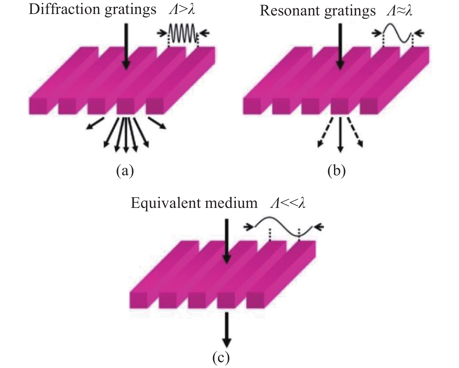
Fig. 1. Dielectric grating at different scales. (a) Diffraction gratings; (b) Resonant (subwavelength) gratings; (c) Equivalent dielectric films
![Proposal of metagratings[7]](/richHtml/irla/2020/49/9/20201039/img_2.jpg)
Fig. 2. Proposal of metagratings[7]
Fig. 4. Narrow-frequency sharp-angular transmission filter structures and the spectrum using cascaded metagratings[28]
Fig. 5. Analytical theory of optical gratings: mode expansion, resonant and interference. (a) Coupled-mode theory[31]; (b) Guided-mode resonance theory[33-34] ; (c) Generalized Kerker effect[35]
Fig. 8. Beam-steering using anisotropic or asymmetric metegrating
Fig. 9. Metagrating based on topology optimization
Fig. 11. (a) Schematic of microfluidic chip with nanostructured and spot-wise functionalized sensor field[78]; (b) Schematic and (c) optical image of the disposable GMR biosensor chip, consisting of a subwavelength grating (a one-dimensional TiO2 grating structure) on a cyclic olefin copolymer substrate and a microfluidic module for handing the injection of fluid sample into the sensing area[80]
Fig. 12. Nanohole array subwavelength grating filters. (a) Transmission spectra of the hole array filters with different side length (a1) 10 μm, (a2) 5 μm, (a3) 2.4 μm, (a4) 1.2 μm[87]; (b) Color logo based on the nanohole array filter[88]; (c) oNanohle array filter integrated with CMOS imaging sensor[89] ; (d) Si subwavelength grating color filters[90]
Fig. 13. One dimensional nanograting color filters. (a) Schematic diagram and (b) the spectra of the ultrathin Ag nanogratings color filters[98];(c) Schematic diagram of the nanograting color filters; (d) Relationship between color spectra and period of the color filter nanograting[100]
Fig. 14. (a) SEM images of silicon nanowire array; (b) Reflection spectra of color filter for different nanowire arrays[105]; (c) Concept schematic of photoelectric detectors based on vertical silicon nanowires; (d) Color image of test objects taken by silicon nanowire arrays[106]
Fig. 15. (a) Schematic configuration and (b) reflection spectral responses of the subtractive CMY color filters incorporating a Si-Al hybrid-ND metasurface formed on a Si substrate[108]; (c) Cross-shaped Si nanoantennas color filters and (d) its transmittance spectra[113]
Fig. 16. (a) Diagram and (b) absorption spectra of the subwavelength grating (sawtooth anisotropic metamaterial thin film)[118]; (c) Diagram of MICM (metal-insulator composite multilayer); (d) Comparison of absorption spectra for different structures[119]
Fig. 17. (a)Absorption spectra of subwavelength grating with nanodisk unit[123]; (b) Field intensity and energy loss of subwavelength grating with nanodisk unit[123]; (c) Absorption spectra of subwavelength grating absorber with multilayered metal-dielectric-metal resonant stacks [131]. (d) Subwavelength grating of Ti-SiO2-Al structure for solar energy absorption film[133]
Fig. 18. (a) Measured absorption spectra of fabricated Ag-SiO2-Ag cross structure of subwavelength grating with different parameters[135]; (b) Extinction spectra using crossed trapezoid array subwavelength metagraing[139]; (c) Absorption spectra of ring array structure[140]; (d) Absorption spectra of subwavelength grating of cone unit structure[145]

Set citation alerts for the article
Please enter your email address
© Copyright 2018-2021 | Chinese Laser Press. All Rights Reserved 沪ICP备15018463号-20