• Chinese Optics Letters
  • Vol. 19, Issue 12, 121404 (2021)
Lingrong Jiang1、2、3, Jianping Liu1、2、3、*, Lei Hu1、2、3, Liqun Zhang1、3, Aiqin Tian1、3, Wei Xiong1、3、4, Xiaoyu Ren1、3, Siyi Huang1、2、3, Wei Zhou1、3, Masao Ikeda1、3, and Hui Yang1、2、3
Author Affiliations
  • 1Suzhou Institute of Nano-tech and Nano-bionics, Chinese Academy of Sciences, Suzhou 215123, China
  • 2School of Nano-tech and Nano-bionics, University of Science and Technology of China, Hefei 230026, China
  • 3Key Laboratory of Nanodevices and Applications, Chinese Academy of Sciences, Suzhou 215123, China
  • 4Nano Science and Technology Institute, University of Science and Technology of China, Hefei 230026, China
  • show less
    DOI: 10.3788/COL202119.121404 Cite this Article Set citation alerts
    Lingrong Jiang, Jianping Liu, Lei Hu, Liqun Zhang, Aiqin Tian, Wei Xiong, Xiaoyu Ren, Siyi Huang, Wei Zhou, Masao Ikeda, Hui Yang. Reduced threshold current density of GaN-based green laser diode by applying polarization doping p-cladding layer[J]. Chinese Optics Letters, 2021, 19(12): 121404 Copy Citation Text show less

    Abstract

    Absorption induced by activated magnesium (Mg) in a p-type layer contributes considerable optical internal loss in GaN-based laser diodes (LDs). An LD structure with a distributed polarization doping (DPD) p-cladding layer (CL) without intentional Mg doping was designed and fabricated. The influence of the anti-waveguide structure on optical confinement was studied by optical simulation. The threshold current density, slope efficiency of LDs with DPD p-CL, and Mg-doped CL, respectively, were compared. It was found that LDs with DPD p-CL showed lower threshold current density but reduced slope efficiency, which were caused by decreasing internal loss and hole injection, respectively.

    1. Introduction

    Visible laser diodes (LDs) based on group III nitride materials have been employed as light sources in many fields such as full-color laser projection, laser lighting, under water communication, and material processing[15]. Despite their considerable commercial success in some areas, great efforts to further decrease threshold current density and to increase slope efficiency of LDs are needed to meet wider application requirements[6]. One of the obstacles hindering progress is the large optical internal loss, including absorption in p-doped layers, absorption by the passive regions, re-absorption of quantum wells (QWs), and absorption and scattering related to chip processing. It is believed that optical absorption loss caused by impurity doping, especially magnesium (Mg) doping, is the main source of internal loss[79]. Kioupakis et al. reported that acceptor-bound hole absorption was the dominant mechanism by theoretical calculation[8]. For the conventional structure of GaN-based LDs, Mg-doped AlGaN is applied as the electron blocking layer (EBL) and p-cladding layer (p-CL). These heavily doped layers have a large overlap with the modal optical field. Optical loss caused by Mg doping in visible LDs is approximately 1015cm1 based on the absorption coefficient data given by Sizov et al.[9], while the typical internal loss of the LDs is about 1530cm1, which means a majority of internal loss originates from the Mg doping layer. Thus, the performance improvements of visible LDs are limited by Mg doping induced internal loss. Decreasing the internal loss can be achieved by reducing the overlap of the waveguide mode with a Mg-doped layer, specifically, shifting the optical field away from the doped layer or decreasing the doping concentration. The movement of the optical field to the n-side may have detrimental impacts on the optical confinement factor of QWs and mode confinement, therefore leading to lower mode gain and a stronger substrate mode[10], respectively. Decreasing the Mg doping concentration directly will increase electrical resistance of the p-type layer because of the low ionization rate of Mg in nitride materials, which can increase forward voltage and decrease injection efficiency.

    Distributed polarization doping (DPD) is a newly proposed technique that can provide holes in nitride materials without Mg doping[11,12]; therefore, it is possible to reduce internal loss by suppressing the Mg doping concentration in p-CL and maintain enough hole concentration at the same time. Currently, the applications on DPD focus on p-CL in ultraviolet (UV) devices and show some inspirational results[1316]. However, decreasing internal loss by DPD in visible LDs has not been reported yet.

    In this article, we designed and fabricated GaN-based green LDs with low threshold current density by employing DPD p-CL. Optical simulations and calculations were introduced to design and analyze the LDs. Device measurements showed the threshold current density of green LDs was reduced by half (from 3.15kA/cm2 to 1.7kA/cm2), while the slope efficiency deteriorated. The possible reason for these changes has been explored.

    2. Experimental Details

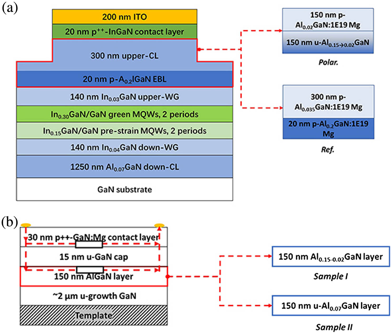
    Two LD structures (named Polar. and Ref. LDs, respectively) were designed, as shown in Fig. 1(a). Low growth temperature and a hybrid p-CL layer were used to suppress the thermal budget to QWs during p-CL growth, which was demonstrated in our previous work[1719]. The layer structure is the same for Ref. LDs and Polar. LDs except for the following part. For Ref. LDs, 300 nm Al0.035GaNp-CL with 1×1019cm3Mg doping and 20 nm Al0.2GaN EBL with 1×1019cm3Mg doping were adopted. For Polar. LDs, the EBL structure was removed, and p-CL consisted of 150 nm undoped AlGaN with Al composition grading from 0.15 to 0.02 and 150 nm Al0.02GaN with 1×1019cm3Mg doping.

    (a) Schematic structures of green Polar. and Ref. LDs, respectively. (b) Sample structure for Hall measurements, the dash line shows the current pathway in measurement.

    Figure 1.(a) Schematic structures of green Polar. and Ref. LDs, respectively. (b) Sample structure for Hall measurements, the dash line shows the current pathway in measurement.

    The theoretical hole concentration p in the DPD structure can be calculated as follows[20]: σ=Ptotal=PspAlGaN+PpzAlGaNPspGaN,PpzAlGaN=2(e31c13c33e33)(aGaNaAlGaNaAlGaN),p=ΔσqΔd,where Δσ is the deviation of net polarization charge densities in the graded layer, e is the piezoelectric constants, c is the elastic constants, a is the lattice constants, q is the elementary charge, and Δd is the layer thickness (in centimeters). Material parameters are taken from Refs. [2123]. According to Eqs. (1)–(3), we can deduce that p5.4×1013·ΔxΔdcm3,where Δx is the Al composition variation. According to Eq. (4), the estimated hole concentration in the designed DPD layer of Polar. LDs is about 4.7×1017cm3. In order to obtain the actual hole concentration of the DPD layer, two samples for Hall measurements are designed, as shown in Fig. 1(b). For sample I, the measured sheet carrier density p1 (7.46×1012cm2) consists of the sheet carrier density of the Al0.150.02GaN and GaN contact layers. For sample II, the measured sheet carrier density p2 (4.12×1012cm2) originates from the GaN contact layer. Then, the net sheet density carrier density of Al0.150.02GaN is p3=p1p2=3.34×1012cm2. The hole concentration in Al0.150.02GaN can be calculated as p=p3/dAlGaN=2.23×1017cm3, which is quite close to the one in conventional Mg doping AlGaN used in Ref. LDs[18] and even smaller than the calculated value.

    3. Results and Discussion

    As the composition-graded layer in Polar. LDs will lead to the anti-waveguide structure, which may influence the optical confinement factor (Γ) and substrate mode intensity, the distribution of the optical field was calculated by commercial optical simulation software named MODE SOLUTION developed by Lumerical Inc. More details on the optical simulations and refractive index data for nitride materials at the green wavelength range can be found in Ref. [10]. The simulation results are shown in Fig. 2. The optical confinement factors of QWs are 0.9143% for Polar. LDs and 0.9269% for Ref. LDs, respectively. The difference of Γ2QWs is quite small, and thus it will not have obvious impacts on the threshold current density or slope efficiency. We can also find that the intensity of the substrate mode increases from 2×10³ to 1.2×10², which means LDs with DPD p-CL may suffer from more severe mode leakage. On the one hand, as the absolute value of the leaked mode and the absorption coefficient of the Si-doped layer are small, the increased substrate mode intensity will not have an obvious impact on LD output power and threshold current density. On the other hand, the enhanced leaked mode will have a negative impact on the far-field pattern of LDs. Both the variation of Γ2QWs and substrate mode intensity can be explained by the prominent movement of the optical field to the n-side in Polar. LD as the result of higher average Al composition in the DPD layer.

    Simulated optical field distribution of (a) LDs with DPD p-CL and (b) LDs with Mg doping p-CL. Insets show the enlarged distribution around p-CL.

    Figure 2.Simulated optical field distribution of (a) LDs with DPD p-CL and (b) LDs with Mg doping p-CL. Insets show the enlarged distribution around p-CL.

    Polar. and Ref. structures, respectively, were grown by metal organic chemical vapor deposition. Inductively coupled plasma dry etching was used to form the ridge waveguide LDs. A 200 nm Si dioxide layer was deposited as the insulating layer using inductively coupled plasma chemical vapor deposition on both sides of the ridges. A 200 nm indium tin oxide (ITO) layer was then deposited on top of the ridge using electron beam evaporation. About 100/500 nm of titanium (Ti)/Au was then deposited on top of ITO as a p pad and 50/100/50/100 nm of Ti/Al/Ti/Au was deposited on the backside of the wafer to form the n electrode. The LD cavity facets were formed by cleaving among the m-plane of the GaN crystal and then depositing dielectric films. Then, the ridge LDs were measured under pulse operation at room temperature, and the results are shown in Fig. 3(a). The structure of LDs was the same as the one described above, and the facet reflectivities were 95% and 70%, respectively. The size of the ridge was 15μm×1200μm. As can be seen in Fig. 3(a), the threshold current density has been reduced obviously (from 3.15kA/cm2 to 1.7kA/cm2). However, the slope efficiency of Polar. LDs decreased greatly compared with that of Ref. LDs (0.07 W/A versus 0.35 W/A). Figure 3(b) shows the lasing spectra of these two LDs. The wavelength difference may be caused by composition variation in InGaN/GaN multi-QWs (MQWs) of these two samples.

    (a) Power-current (P-I) curves and (b) laser spectra of green LDs with DPD and conventional Mg doping p-CL, respectively. The solid line in (a) is a guide for the eye.

    Figure 3.(a) Power-current (P-I) curves and (b) laser spectra of green LDs with DPD and conventional Mg doping p-CL, respectively. The solid line in (a) is a guide for the eye.

    Then, the reason for improved threshold current density and deteriorative slope efficiency was explored. According to Refs. [24,25], the threshold current density and slope efficiency of the LDs could be expressed as follows: Jth=Jtrηiηinj·exp(αi+αmΓ2QWsg0),S.E.=hcqλ·αmαm+αi·ηiηinj,αm=12Lln(1R1R2),where Jtr, ηi, ηinjαi, L, R, g0, h, c, q, and λ are the transparent current density, internal quantum efficiency, injection efficiency, internal loss, cavity length (L=1200μm), reflectivity of facet, material gain coefficients, Planck constant, speed of light, electron charge, and wavelength of light, respectively. The transparent current density was assumed to be 0.4kA/cm2, which is higher than the reported one for blue LDs[26]. The values of injection efficiency and internal quantum efficiency were 90% and 75%, respectively, based on the measurements of our LDs. The material gain was set as 660cm1 according to our measurements and this value is close to the one demonstrated by Ref. [27]. For the absorption in p-doped, n-doped, and ITO layers, we assumed absorption coefficients α0 of 50cm1, 10cm1[28], and 2000cm1[19], respectively. Then, the total internal loss can be calculated by αi=Γ·α0.

    Applying Eq. (8), the total internal loss in Polar. and Ref. LDs was 4.67cm1 and 9.57cm1, respectively. It should be pointed out that only 150 nm conventional Mg doping p-CL near the QW side had been replaced by the DPD layer, and EBL had been removed, but the internal loss of Polar. LDs was almost 50% smaller than that of the Ref. LDs. These results can be well understood by the significant suppression of the overlap of the optical field and Mg doping layer. This indicated the great potential of DPD in decreasing internal loss in nitride LDs. Thus, the threshold current density and slope efficiency can be calculated by Eqs. (5)–(7): 1.67kA/cm2 and 0.43 W/A for Polar. LDs, 3.71kA/cm2 and 0.25 W/A for Ref. LDs, respectively. The predicted 50% reduction in threshold current density agrees well with the measurement results.

    Since we have confirmed Polar. LDs have smaller internal loss, it is reasonable to speculate that the decreasing injection efficiency is the reason for deteriorative slope efficiency according to Eq. (6). Figure 4 shows the temperature dependent photoluminescence (TDPL) result of Polar. LDs, which indicates that the internal quantum efficiency is 50%. Thus, the injection efficiency is 22%. This value is pretty low compared with the estimated one in the calculations (90%). Actually, GaN-based LDs with DPD p-CL show that very low injection efficiency have also been demonstrated in UV-C devices[29], although, in theory, DPD p-CL is expected to provide relatively high hole concentration without Mg doping[30]. It is worth noting that Hall measurements based on the Van der Pauw method are usually applied to extract the carrier information of a single layer. However, the information given by this method corresponds to horizontal transportation in the films, which is different from the situation in actual devices (carrier transport in vertical direction). Thus, even though we can obtain relatively good conductivity (high hole concentration and mobility) for single layers, the hole injection in the vertical direction may be a problem. Figure 5 presents the I-V curves of Polar. and Ref. LDs. It can be seen that the turn-on voltage of Polar. LDs is 6 V, which is about 2 V higher than that of the Ref. LDs. The higher turn-on voltage suggests that there are potential barriers in Polar. LDs.

    TDPL result of Polar. LD. The solid line is the result of Arrhenius fitting.

    Figure 4.TDPL result of Polar. LD. The solid line is the result of Arrhenius fitting.

    Current-voltage (I-V) curves of green LDs with DPD and Mg doping p-CL, respectively.

    Figure 5.Current-voltage (I-V) curves of green LDs with DPD and Mg doping p-CL, respectively.

    The cause for low injection efficiency has not been figured out yet, and some suppositions have been given in literatures. The consumption induced by point defects in Al-rich AlGaN had been attributed to one of the reasons in UV LDs[29]. However, considering the average Al composition is only about 8% for our samples, which is far less than that in UV devices, the material quality should not be the main problem. Another possible reason may be the carrier spillover. Sato et al. demonstrated that UV-B LDs with DPD p-CL had spontaneous subpeak emission, which could consume injected carriers by recombination at the potential minimum formed at the interface of the waveguide layer (WG) and EBL because of large polarization discontinuity[31]. Unfortunately, this interpretation cannot explain our cases, as the polarization discontinuity between WG and EBL (acted by the DPD p-CL because the Al composition near the WG is as large as 15%) in the Polar. LD is even smaller than that in the Ref. LD since the Al composition is smaller (15% versus 20%), and we also did not observe any subpeak in the photoluminescence measurement, as shown in Fig. 3(b). Reference [32] demonstrated that blue LEDs with DPD EBL showed higher turn-on voltage and lower injection efficiency compared with the reference samples, although high hole concentration in a composition-graded AlGaN had been observed clearly by separate Hall measurement[20]. It is believed that polarization charges at the interface can induce dips or spikes in energy band profiles, hindering holes injection. Then, the polarization doping concept was proposed, while the performances of LEDs with DPD are still inferior to the references at low injection currents. Since DPD is realized by inducing high concentration net negative polarization charges in film to attract holes, those fixed charges may have a detrimental effect on the carrier transportation, which needs further study to confirm. It is worth pointing out that the hole concentration for our structure is 2.23×1017cm3, which can be increased by applying larger Al composition. The increased hole concentration is helpful to improve hole injection.

    4. Conclusions

    GaN-based green LDs with DPD and Mg doping p-CL, respectively, were designed and fabricated. LDs with DPD p-CL showed reduced threshold current density but lower slope efficiency. Reduction of internal loss by DPD is the main reason for decreasing the threshold current density. The low slope efficiency is attributed to small low injection efficiency, which may be caused by poor hole transportation in the vertical direction. This research proves the possibility to decrease threshold current density by DPD, while further work to improve hole injection is needed.

    References

    [1] H. Wang, Y. Kawahito, R. Yoshida, Y. Nakashima, K. Shiokawa. Development of a high-power blue laser (445 nm) for material processing. Opt. Lett., 42, 2251(2017).

    [2] S. Nagahara. Three primary color LD module. SID Symp. Digest Tech. Papers, 48, 80(2017).

    [3] X. Liu, S. Yi, X. Zhou, Z. Fang, Z.-J. Qiu, L. Hu, C. Cong, L. Zheng, R. Liu, P. Tian. 34.5 m underwater optical wireless communication with 2.70 Gbps data rate based on a green laser diode with NRZ-OOK modulation. Opt. Express, 25, 27937(2017).

    [4] X. Huang, F. Yang, J. Song. Hybrid LD and LED-based underwater optical communication: state-of-the-art, opportunities, challenges, and trends. Chin. Opt. Lett., 17, 100002(2019).

    [5] L.-K. Chen, Y. Shao, R. Deng. Robust UOWC systems against bubble-induced impairments via transmit/receive diversities. Chin. Opt. Lett., 17, 100006(2019).

    [6] H. König, M. Ali, W. Bergbauer, J. Brückner, G. Brüderl, C. Eichler, S. Gerhard, U. Heine, A. Lell, L. Naehle, M. Peter, J. Ristic, G. Rossbach, A. Somers, B. Stojetz, S. Tautz, J. Wagner, T. Wurm, U. Strauss, M. Baumann, A. Balck, V. Krause. Visible GaN laser diodes: from lowest thresholds to highest power levels. Proc. SPIE, 10939, 109390C(2019).

    [7] E. Kioupakis, P. Rinke, C. G. Van de Walle. Determination of internal loss in nitride lasers from first principles. Appl. Phys. Express, 3, 082101(2010).

    [8] E. Kioupakis, P. Rinke, A. Schleife, F. Bechstedt, C. G. Van de Walle. Free-carrier absorption in nitrides from first principles. Phys. Rev. B, 81, 241201(2010).

    [9] D. Sizov, R. Bhat, C.-E. Zah. Optical absorption of Mg-doped layers and InGaN quantum wells on c-plane and semipolar GaN structures. J. Appl. Phys., 113, 203108(2013).

    [10] L. Jiang, J. Liu, L. Zhang, B. Qiu, A. Tian, L. Hu, D. Li, S. Huang, W. Zhou, M. Ikeda, H. Yang. Suppression of substrate mode in GaN-based green laser diodes. Opt. Express, 28, 15497(2020).

    [11] J. Simon, V. Protasenko, C. Lian, H. Xing, D. Jena. Polarization-induced hole doping in wide-band-gap uniaxial semiconductor heterostructures. Science, 327, 60(2010).

    [12] S. Li, M. E. Ware, J. Wu, V. P. Kunets, M. Hawkridge, P. Minor, Z. Wang, Z. Wu, Y. Jiang, G. J. Salamo. Polarization doping: reservoir effects of the substrate in AlGaN graded layers. J. Appl. Phys., 112, 053711(2012).

    [13] O. V. Khokhlev, K. A. Bulashevich, S. Y. Karpov. Polarization doping for III-nitride optoelectronics. Phys. Status Solidi A, 210, 1369(2013).

    [14] Z. Zhang, M. Kushimoto, T. Sakai, N. Sugiyama, L. J. Schowalter, C. Sasaoka, H. Amano. A 271.8 nm deep-ultraviolet laser diode for room temperature operation. Appl. Phys. Express, 12, 124003(2019).

    [15] K. Sato, S. Yasue, Y. Ogino, S. Tanaka, M. Iwaya, T. Takeuchi, S. Kamiyama, I. Akasaki. Light confinement and high current density in UVB laser diode structure using Al composition-graded p-AlGaN cladding layer. Appl. Phys. Lett., 114, 191103(2019).

    [16] D. Zhao. III-nitride based ultraviolet laser diodes. J. Semicond., 40, 120402(2019).

    [17] Z. Li, J. Liu, M. Feng, K. Zhou, S. Zhang, H. Wang, D. Li, L. Zhang, D. Zhao, D. Jiang, H. Wang, H. Yang. Suppression of thermal degradation of InGaN/GaN quantum wells in green laser diode structures during the epitaxial growth. Appl. Phys. Lett., 103, 152109(2013).

    [18] A. Tian, J. Liu, M. Ikeda, S. Zhang, Z. Li, M. Feng, K. Zhou, D. Li, L. Zhang, P. Wen, F. Zhang, H. Yang. Conductivity enhancement in AlGaN:Mg by suppressing the incorporation of carbon impurity. Appl. Phys. Express, 8, 051001(2015).

    [19] L. Hu, X. Ren, J. Liu, A. Tian, L. Jiang, S. Huang, W. Zhou, L. Zhang, H. Yang. High-power hybrid GaN-based green laser diodes with ITO cladding layer. Photon. Res., 8, 279(2020).

    [20] T. Yasuda, K. Yagi, T. Suzuki, T. Nakashima, M. Watanabe, T. Takeuchi, M. Iwaya, S. Kamiyama, I. Akasaki. Investigations of polarization-induced hole accumulations and vertical hole conductions in GaN/AlGaN heterostructures. Jpn. J. Appl. Phys., 52, 08JJ05(2013).

    [21] F. Bernardini, V. Fiorentini, D. Vanderbilt. Spontaneous polarization and piezoelectric constants of III-V nitrides. Phys. Rev. B, 56, R10024(1997).

    [22] M. Asif Khan, A. Bhattarai, J. N. Kuznia, D. T. Olson. High electron mobility transistor based on a GaN-AlxGa1−xN heterojunction. Appl. Phys. Lett., 63, 1214(1993).

    [23] K. Kim, W. R. L. Lambrecht, B. Segall. Elastic constants and related properties of tetrahedrally bonded BN, AlN, GaN, and InN. Phys. Rev. B, 53, 16310(1996).

    [24] L. A. Coldren, S. W. Corzine, M. L. Mašanović. A phenomenological approach to diode lasers. Diode Lasers and Photonic Integrated Circuits(2012).

    [25] M. Kawaguchi, O. Imafuji, S. Nozaki, H. Hagino, S. Takigawa, T. Katayama, T. Tanaka. Optical-loss suppressed InGaN laser diodes using undoped thick waveguide structure. Proc. SPIE, 9748, 974818(2016).

    [26] H. Y. Ryu, K. H. Ha, J. K. Son, S. N. Lee, H. S. Paek, T. Jang, Y. J. Sung, K. S. Kim, H. K. Kim, Y. Park, O. H. Nam. Determination of internal parameters in blue InGaN laser diodes by the measurement of cavity-length dependent characteristics. Appl. Phys. Lett., 93, 011105(2008).

    [27] D. J. Kunzmann, R. Kohlstedt, T. Uhlig, U. T. Schwarz. Critical discussion of the determination of internal losses in state-of-the-art (Al, In)GaN laser diodes. Proc. SPIE, 11280, 112800Y(2020).

    [28] M. Kuramoto, C. Sasaoka, N. Futagawa, M. Nido, A. A. Yamaguchi. Reduction of internal loss and threshold current in a laser diode with a ridge by selective re-growth (RiS-LD). Phys. Status Solidi A, 192, 329(2002).

    [29] Z. Zhang, M. Kushimoto, T. Sakai, N. Sugiyama, L. J. Schowalter, C. Sasaoka, H. Amano. Design and characterization of a low-optical-loss UV-C laser diode. Jpn. J. Appl. Phys., 59, 094001(2020).

    [30] Z. Zhang, M. Kushimoto, M. Horita, N. Sugiyama, L. J. Schowalter, C. Sasaoka, H. Amano. Space charge profile study of AlGaN-based p-type distributed polarization doped claddings without impurity doping for UV-C laser diodes. Appl. Phys. Lett., 117, 152104(2020).

    [31] K. Sato, S. Yasue, Y. Ogino, M. Iwaya, T. Takeuchi, S. Kamiyama, I. Akasaki. Analysis of spontaneous subpeak emission from the guide layers of the ultraviolet-B laser diode structure containing composition-graded p-AlGaN cladding layers. Phys. Status Solidi A, 217, 1900864(2020).

    [32] T. Yasuda, K. Hayashi, S. Katsuno, T. Takeuchi, S. Kamiyama, M. Iwaya, I. Akasaki, H. Amano. Polarization dilution in a Ga-polar UV-LED to reduce the influence of polarization charges. Phys. Status Solidi A, 212, 920(2015).

    Lingrong Jiang, Jianping Liu, Lei Hu, Liqun Zhang, Aiqin Tian, Wei Xiong, Xiaoyu Ren, Siyi Huang, Wei Zhou, Masao Ikeda, Hui Yang. Reduced threshold current density of GaN-based green laser diode by applying polarization doping p-cladding layer[J]. Chinese Optics Letters, 2021, 19(12): 121404
    Download Citation