Abstract
Full-color displays based on micro light-emitting diodes (μLEDs) can be fabricated on monolithic epitaxial wafers. Nanoring (NR) structures were fabricated on a green LED epitaxial wafer; the color of NR-μLEDs was tuned from green to blue through strain relaxation. An Al2O3 layer was deposited on the sidewall of NR-μLEDs, which improved the photoluminescence intensity by 143.7%. Coupling with the exposed multiple quantum wells through nonradiative resonant energy transfer, red quantum dots were printed to NR-μLEDs for a full-color display. To further improve the color purity of the red light, a distributed Bragg reflector is developed to reuse the excitation light.1. INTRODUCTION
The use of micro light-emitting diodes (μLEDs) and quantum dots (QDs) has expanded rapidly in recent years [1,2]. μLEDs and QDs are expected to replace thin-film transistor liquid crystal displays (TFT-LCDs) and organic LEDs due to their compact size, high efficiency, and reliability [3,4]. Full-color μLED displays can be assembled into red-green-blue (RGB) LED matrices through mass-transfer technology [5]. However, this technology is not ready for commercialization and mass production of μLEDs due to challenges, including low transfer yield, slow transfer time, high fabrication cost, difficulty of inspection, and difficulty of repair [6,7]. Consequently, some researchers have combined single-color (near UV) LED arrays and RGB QDs to avoid the mass-transfer process [8,9]. In addition to using QDs for color conversion, another method to manufacture LEDs of different colors is strain-induced engineering. The method of strain-induced engineering involves reducing the volume of the LEDs by an etching process, resulting in the release of strain and reduction of the quantum-confined Stark effect [10]. This effect simultaneously flattens the tilted energy band, increases the overlap of the quantum state distributions, and blueshifts the wavelength [11].
A previous study by the current authors demonstrated a wavelength tunable nanoring μLED (NR-μLED) by strain-induced engineering; that study demonstrated that the color of an NR-μLED could be precisely tuned from green to blue by controlling the wall width of the NR-μLED through etching [12]. Moreover, a color conversion method was designed to produce full-color high-quality μLED displays by combining UV μLEDs and RGB QDs [13,14]. Although these studies have gained considerable recognition, the performance of the devices in these studies can be further improved.
First, the studied NR-μLEDs had diameters smaller than 1 μm [12]. The peak external quantum efficiency (EQE) for a device of such a small diameter is markedly low [15]. This low EQE is due to the surface recombination and sidewall damage to the mesa from the plasma-assisted dry etching, which creates sidewall defects to produce recombination centers [16]. Sidewall passivation by using dielectric materials is an effective method to limit plasma damage in LEDs [17]. Compared with the conventional sidewall passivation approach using plasma-enhanced chemical vapor deposition, atomic layer deposition (ALD) can form a high-density dielectric film with a thickness of a few ångströms that acts as an effective passivation layer [18]. ALD provides a wide range of solutions to modern lighting industries to achieve superior device performance and long lifetimes.
Second, full-color displays in our previous studies [13,14] were based on UV μLEDs radiatively pumping RGB QDs with restricted color conversion efficiency due to considerable spatial separation between multiple quantum wells (MQWs) and QDs. To overcome this drawback, nonradiative resonant energy transfer (NRET) was proposed as another method for effective color conversion [19]. NRET is an interaction between acceptors and donors in which the excitation energy of a donor is transferred to an acceptor [20]. NRET requires three factors: (1) the acceptors’ absorption spectrum should overlap the donors’ fluorescence emission spectrum, (2) the transition of dipole orientation must be parallel, and (3) the separation of donor and acceptor excitons must be sufficiently small (typically ) [20,21]. In similar cases, the MQWs of a lighting device act as donors, whereas the QDs act as acceptors [20–23].
This study reports hybrid quantum dot nanoring micro LEDs (QD-NR-μLEDs) fabricated through electron beam (E-beam) lithography and QD printing. This device is composed of three parts, namely, a normal green LED, a blue NR-μLED, and a red QD-NR-μLED; each region can be regarded as a subpixel. Our previous study compared single-color LED arrays with wavelength-tunable nanoring LEDs produced by strain-induced engineering; that work provided a solution to create green and blue light using μLEDs [12]. Printing red QDs on blue NR-μLEDs is an excellent method to provide full-color μLED displays, allowing adjacent coupling between the QDs and the exposed InGaN/GaN MQW sidewalls through the NRET mechanism. To reduce the emissive intensity loss caused by sidewall defects, an ALD passivation layer can be introduced into the process. With ALD, the thickness of the ultrathin passivation layer between MQWs and QDs can be controlled; thus, NRET efficiency can be maintained. Therefore, color conversion from NR-μLEDs to QDs results in excellent optical properties and confers excellent color features on hybrid QD-NR-μLEDs.
2. EXPERIMENT
Figure 1 depicts the process flow of the hybrid QD-NR-μLEDs and the cross-sectional view of the completed device. In this process, the epitaxial layers of InGaN/GaN LEDs with an emission wavelength of 525 nm were grown on c-plane pattern sapphire substrates through metal organic chemical vapor deposition. The epitaxial structure consisted of a GaN buffer layer (3 μm), an n-GaN layer (1.5 μm), an undoped InGaN/GaN MQW active layer, and a p-GaN layer (150 nm). The MQWs were constructed using eight pairs of 4-nm-thick wells and a 12-nm-thick GaN barrier. The fabrication process started from the bare epitaxial wafer after standard cleaning, as shown in Fig. 1(a). The lithography process was conducted using an E-beam lithography system with a specialized photoresist. In the first step, an E-beam process was used to define an RGB region with negative photoresist. The area of each region of subpixels was , and each green subpixel was shaped in a normal rectangular mesa. The other two regions constituted the NR array (which had hexagonal close packing). The outer and inner diameters of an NR are 900 and 700 nm, respectively. Subsequently, nickel was deposited through E-beam evaporation, and then the photoresist was removed through a lift-off process to form a hard mask pattern. Next, inductively coupled plasma reactive ion etching (ICP-RIE) was used to etch the GaN-based material to define the active area, separate the pn layer, and isolate each subpixel. Then, HCl solution was used to remove the residual nickel. For the passivation layer of the hybrid QD-NR-μLEDs, the ALD technology was used in this experiment. The passivation layer was grown at 300°C in argon (Ar) ambience by applying the cycle for 0.1 s for trimethylaluminum (TMA) and for 0.1 s for , with 7 s of Ar purging. The passivation layer thickness could be accurately controlled using the cycle numbers. To create the color conversion layer, CdSe/ZnS red QDs were sprayed on a region of blue NR-μLED through the super-inkjet (SIJ) printing system (SIJ Technology, Inc.). The results of the aforementioned completion process are shown in Fig. 1(b), and the study uses samples from this step for optical analysis. After the color conversion layer process, spin-on glass (SOG) was used to protect the QD layer and isolate the pn electrodes. Next, a transparent conducting oxide (TCO) layer was sequentially deposited through the hole process by SOG etching and Ni/Au metal deposition for the pn electrodes with the lift-off process, as depicted in Fig. 1(c). Finally, a distributed Bragg reflector (DBR) was used to cover the red color region to filter out and recycle blue light, as illustrated in Fig. 1(d). Figure 1(e) depicts the full-color display panel composed of the proposed hybrid QD-NR-μLEDs, and Fig. 1(f) demonstrates the cross-sectional view for a single pixel.
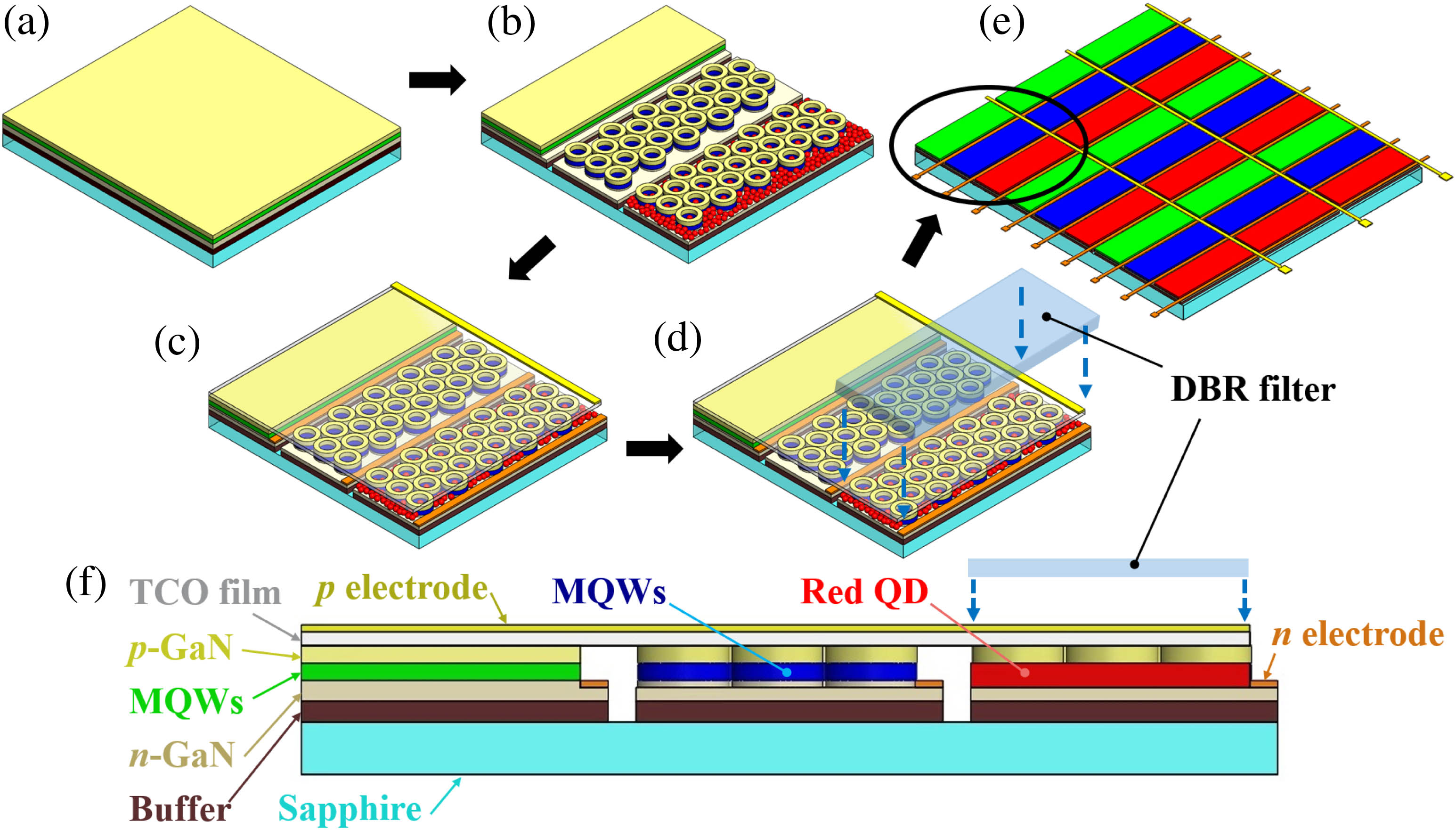
Figure 1.(a) Epitaxial wafer; (b) three subpixels of a green μLED, a blue NR-μLED, and a red QD-NR-μLED; (c) deposition of TCO film and pn electrodes; (d) covering DBR filter; (e) full-color display panel composed of the proposed hybrid QD-NR-μLEDs; (f) cross-sectional view of a single RGB pixel.
3. RESULTS AND DISCUSSION
For the optical characteristics, a photoluminescence (PL) system was implemented using a 375-nm solid-state laser source. Figure 2(a) illustrates the PL emission spectra of the blue NR-μLED with and without an passivation layer deposited through ALD. The emission intensity of the NR-μLED from 430 to 515 nm increased by 143.7% with a 1-nm-thick passivation layer. This increase could be explained by the reduction of the total internal reflection (TIR) from optical characteristics [18] and the reduction of nonradiative recombination caused by surface trapping and defects. The refractive index of the film deposited by ALD was 1.72, which was between that of air () and GaN (). The critical angle of TIR can be described as . is the critical angle for TIR to occur if the light incident on the border has an angle less than , is the refractive index of the medium of high refractive index, and is the refractive index of the medium of low refractive index. When the difference of refractive index between the two materials is reduced, increases, which indicates that light coming from a different angle could travel through the boundary.

Figure 2.(a) PL emission spectra of NR-μLEDs with and without ALD passivation; (b) TD-TRPL curves of NR-μLEDs with and without ALD passivation at 15 K and 300 K, respectively.
Moreover, Fig. 2(b) displays the temperature-dependent time-resolved photoluminescence (TD-TRPL) decay curve of NR-μLEDs with and without ALD passivation. TD-TRPL measurement was conducted at extremely low power (20 μW) for a very low excitation power density to prevent many-body effects, thus ensuring that excitonic recombination dominated InGaN/GaN MQWs. A pulse width-defined rise in the transmission signal followed by a PL decay indicates that this curve concurred with the double-exponential function resulting from multiple recombination centers [24]. The decay parameter can be extracted from a regular double-exponential fit, in which a two-component PL decay is described through two-influence elements. The first element is attributed to the relaxation of localized excitons, and the second element is the exciton relaxation of free-carriers and localized states, which is strongly related to defect recombination [25]. The normalized TRPL trace is given as follows: where and define the fraction of electron-hole pairs that do not undergo and do undergo NRET, respectively. The radiative and nonradiative terms and define the decay lifetime of two terms corresponding to localized excitons and exciton relaxation of free-carriers and localized states.
According to the exponential decay fitting, the total recombination time () of each curve was 10.40, 7.80, 3.03, and 2.28 ns, corresponding to the measurement temperatures at 15 K and 300 K for the NR-μLED without passivation and with passivation. In the 15 K environment, the radiative recombination mechanism was dominant, but the influence of nonradiative recombination centers still existed even when it declined. This explains why the lifetime of an NR-μLED at 15 K is longer than that of a device at 300 K (the freeze-out of the nonradiative recombination centers can be attributed to the surface defect state) [24]. The short lifetime at 15 K for the sample with passivation indicates a superior radiative recombination process because of the reduction of surface defects. The same results at 300 K were observed for a sample with passivation. However, nonradiative recombination centers dominated the recombination mechanism at 300 K [26]. Therefore, in Fig. 2(a), in addition to the blue peak enhancement of the NR-μLED with the passivation layer, the intensity of the long-wavelength peak (from 515 to 730 nm), which represents the contribution of defects in the spectrum, is weakened by 13.9%. The results show that, in addition to improving the reliability of electronic components, the ALD passivation process can considerably improve the optical-electric characteristics of μLEDs because the increase of the surface-to-volume ratio reduced the surface defect state.
In our previous study, the minimum linewidth of deposited QDs through aerosol jet printing was limited to 30–40 μm [14]. When the size of each subpixel is reduced to , the previous method would no longer be applicable. Therefore, we upgraded the QD spray method to improve the spray accuracy and reduce the deposition linewidth. Figure 3(a) displays NCTU (National Chiao Tung University), SCLAB (Semiconductor Laser and LED Laboratory), and XMU (Xiamen University) patterns printed in red QDs on glass with the latest SIJ printing system, and the linewidth of 1.65 μm was measured through fluorescence microscopy (FLOM). The FLOM image depicts a clear line shape and excellent uniformity. Moreover, the turning point was handled quite perfectly. Additionally, atomic force microscopy (AFM) results depicted in Fig. 3(b) display a 3D image that clearly demonstrates the surface profile of deposited QDs. Figure 3(b) precisely depicts that the deposited QDs (the bulged line) had a height of 56.3 nm and a linewidth of less than 2 μm. Therefore, using the SIJ printing system, we can accurately spray red QDs on a subpixel area of a blue NR-μLED to achieve red-light emission.
Figure 3.(a) FLOM image of patterns printed by red QDs on a glass by using the latest SIJ printing system (the inset depicts minimum linewidth); (b) AFM image of deposited QDs.
Figure 4 demonstrates the overlapping relationship of the electroluminescence (EL) spectrum of a blue NR-μLED and the absorption spectrum of red QDs. The emission wavelength of the blue NR-μLED is 467 nm and is in the range of intense QD absorption, indicating good spectral overlaps of MQWs with QD absorption and guaranteeing strong coupling between the excitons in MQWs and the absorption dipoles of QDs [20]. In addition, Fig. 4 displays the schematic of spraying red QDs on blue NR-μLEDs by using the SIJ printing system.
Figure 4.Absorption curve of red QDs and electroluminescence (EL) spectrum of blue NR-μLEDs (inset depicts a schematic configuration of spraying red QDs on blue NR-μLEDs using the SIJ printing system).
Investigation of fabricated NR-μLEDs was conducted through scanning electron microscopy (SEM). The SEM images are demonstrated in Figs. 5(a) and 5(b) with different scales and view angles. Furthermore, from transmission electron microscopy (TEM) images in Fig. 5(c), we could clearly observe that the sidewalls of InGaN/GaN MQWs were closely surrounded by QDs, as expected, which is essential for the NRET mechanisms. The morphology of red QDs with diameters of approximately 10 nm can be observed in the same figure. In addition, a 1-nm-thick layer of deposited on the sidewall of NR-μLEDs is evident in the TEM image in Fig. 5(d).
Figure 5.(a) SEM image of RGB pixel array (top view); (b) SEM image of NR-μLED with 30° tilt angle; (c) TEM image of the contact area between MQWs and QDs; (d) TEM image of 1 nm deposited on the sidewall of an NR-μLED through ALD.
Figure 6(a) presents the experimental observations of QD-NR-μLED energy transfer. For measurement and quantification of the transfer of energy from NR-μLEDs to QDs, the PL dynamics in the MQWs of NR-μLEDs were monitored using typical room temperature TRPL. The decay curve of a QD-NR-μLED was lower than that of the reference NR-μLED, as illustrated in Fig. 6(a). This tendency cannot be observed if no NRET mechanism is relevant [20]. The NRET coupling in QD-NR-μLEDs generates a variation in decay dynamics. The decay rate of InGaN/GaN MQWs can be defined as (which is equal to ) and is dependent on the radiative term () and nonradiative term (), indicated explicitly as follows: An additional energy transfer path is introduced to explore the NRET efficiency in detail, which indicates that the hybrid recombination rate requires modification for the NRET decay rate [27], indicated explicitly as follows: NRET efficiency, , can be determined from the decay rate between an NR-μLED and a QD-NR-μLED using the following equation [28]: From Fig. 6(a), the decay lifetime can be calculated based on fitting using Eq. (1); the decay lifetimes of and are 3.03 ns and 1.02 ns, respectively; and , given an energy transfer rate of through Eqs. (2) and (3). Moreover, the NRET rate is , which is superior to the MQW nonradiative decay rate of . It indicates that the efficient NRET process considerably reduced the nonradiative recombination losses [27]. In Fig. 6(a), the NRET efficiency of the QD-NR-μLED was 66.4%, while the NRET efficiency of the QD-NR-μLED with 1-nm passivation was 53.6% in Fig. 6(b). Additionally, in Figs. 6(a) and 6(b), 19.7% and 17.3% of the MQW exciton population is found to participate in NRET before and after the ALD passivation, respectively. These reductions in efficiency and population were caused by the increase in distance between MQWs and QDs; the dipole-dipole separation weakened the NRET. Notably, the 1-nm-thick passivation layer enhanced the blue light intensity by 143.7% and reduced the NRET efficiency and the population of electron-hole pairs undergoing NRET by only 12.8% and 2.4%, respectively. The NRET mechanism primarily depends on the coupling distance between donors and acceptors, namely, the QDs and MQWs of the NR-μLED in this case. The separated distance between donors and acceptors that can allow the NRET to occur is typically less than 10 nm [19,20,29]. In general, NRET efficiency is inversely proportional to the th power of the distance, and the value of (typically from 4 to 6) typically depends on the material dimensions of donors and acceptors [20,30]. This natural limitation highlights the importance of ALD, which enables precise control of deposition thickness and excellent passivation performance.
Figure 6.(a) Without ALD passivation, TRPL curves of NR-μLEDs with and without red QDs; (b) with 1-nm ALD passivation, TRPL curves of NR-μLEDs with and without red QDs.
To induce emission of pure red light from a QD-NR-μLED region, a DBR was covered on the region as a filter to increase the reuse of blue photons. Figure 7 displays the reflection spectrum of the DBR in the visible light region. The reflectance for 470 nm blue light is close to 95%, while the reflectance for 630 nm red light is only 8.3%. The reflectance curve of the DBR strongly indicates that the short-wavelength light reflected by the DBR can be used to re-excite the QDs, further improving the efficiency of color conversion [13,14].
Figure 7.Reflectance spectrum of the DBR.
The EL spectra of individual RGB color in hybrid QD-NR-μLEDs are shown in Fig. 8(a) with peak wavelengths at 630, 525, and 467 nm. Additionally, the peak EQEs of the green and blue subpixels are 16% and 15%, respectively. According to the EL spectra, the color coordinates of RGB full-color monolithic hybrid QD-NR-μLEDs are (0.6947, 0.3051), (0.2153, 0.6952), and (0.1313, 0.0708) in the CIE 1931 chromaticity diagram. Moreover, our proposed QD-NR-μLEDs can achieve a wide color gamut because of the narrow EL spectra [in Fig. 8(b)]. For example, the color gamut overlap of the National Television System Committee (NTSC) space is approximately 104.8% and that of Rec. 2020 is 78.2%; these values are sufficient to support full-color performance in display technology.
Figure 8.(a) EL spectra of RGB hybrid QD-NR-μLEDs; (b) color gamut of RGB hybrid QD-NR-μLEDs, NTSC, and Rec. 2020.
4. CONCLUSION
In conclusion, a hybrid QD-NR-μLED with an ALD passivation layer and efficient NRET has been fabricated to produce a monolithic RGB μLED device. Its ALD passivation layer provided excellent thickness control and surface defects repair capability to enhance the light-emitting intensity by 143.7%. A minimized separation of donor and acceptor excitons was generated using this novel structure design. Considerable reduction was achieved in the exciton recombination lifetime of the NR-μLEDs in the hybrid device because the NRET mechanism had been observed in the TRPL experiments. The obtained NRET efficiency values of the QD-NR-μLED with and without ALD passivation were 66.4% and 53.6%, respectively. Finally, a wide color gamut determined by the overlap area of NTSC and Rec. 2020 indicates excellent color performance of the hybrid QD-NR-μLED.
Acknowledgment
Acknowledgment. The authors would like to thank the MOST, PICOSUN for their ALD technical support, and the group of Prof. Ji-Lin Shen from Chung Yuan Christian University for the photoluminescence-related measurement support. The authors declare that there are no conflicts of interest related to this paper.
References
[1] Y. Shirasaki, G. J. Supran, M. G. Bawendi, V. Bulovic. Emergence of colloidal quantum-dot light-emitting technologies. Nat. Photonics, 7, 13-23(2013).
[2] H. X. Jiang, J. Y. Lin. Nitride micro-LEDs and beyond--a decade progress review. Opt. Express, 21, A475-A484(2013).
[3] H.-W. Chen, J.-H. Lee, B.-Y. Lin, S. Chen, S.-T. Wu. Liquid crystal display and organic light-emitting diode display: present status and future perspectives. Light Sci. Appl., 7, 17168(2017).
[4] F. Templier. GaN-based emissive microdisplays: a very promising technology for compact, ultra-high brightness display systems. J. Soc. Inf. Disp., 24, 669-675(2016).
[5] B. Corbett, R. Loi, W. D. Zhou, D. Liu, Z. Q. Ma. Transfer print techniques for heterogeneous integration of photonic components. Prog. Quantum Electron., 52, 1-17(2017).
[6] T. Z. Wu, C.-W. Sher, Y. Lin, C.-F. Lee, S. J. Liang, Y. J. Lu, S.-W. Huang Chen, W. J. Guo, H.-C. Kuo, Z. Chen. Mini-LED and micro-LED: promising candidates for the next generation display technology. Appl. Sci., 8, 1557(2018).
[7] L. L. Zheng, Z. Q. Guo, W. Yan, Y. Lin, Y. J. Lu, H. C. Kuo, Z. Chen, L. H. Zhu, T. Z. Wu, Y. L. Gao. Research on a camera-based microscopic imaging system to inspect the surface luminance of the micro-LED array. IEEE Access, 6, 51329-51336(2018).
[8] K. J. Chen, H. C. Chen, K. A. Tsai, C. C. Lin, H. H. Tsai, S. H. Chien, B. S. Cheng, Y. J. Hsu, M. H. Shih, C. H. Tsai, H. H. Shih, H. C. Kuo. Resonant-enhanced full-color emission of quantum-dot-based display technology using a pulsed spray method. Adv. Funct. Mater., 22, 5138-5143(2012).
[9] K. H. Lee, C. Y. Han, H. D. Kang, H. Ko, C. Lee, J. Lee, N. Myoung, S. Y. Yim, H. Yang. Highly efficient, color-reproducible full-color electroluminescent devices based on red/green/blue quantum dot-mixed multilayer. ACS Nano, 9, 10941-10949(2015).
[10] J. H. Ryou, P. D. Yoder, J. P. Liu, Z. Lochner, H. Kim, S. Choi, H. J. Kim, R. D. Dupuis. Control of quantum-confined Stark effect in InGaN-based quantum wells. IEEE J. Sel. Top. Quantum Electron., 15, 1080-1091(2009).
[11] Q. Wang, J. Bai, Y. P. Gong, T. Wang. Influence of strain relaxation on the optical properties of InGaN/GaN multiple quantum well nanorods. J. Phys. D, 44, 395102(2011).
[12] S. W. Wang, K. B. Hong, Y. L. Tsai, C. H. Teng, A. J. Tzou, Y. C. Chu, P. T. Lee, P. C. Ku, C. C. Lin, H. C. Kuo. Wavelength tunable InGaN/GaN nano-ring LEDs via nano-sphere lithography. Sci. Rep., 7, 42962(2017).
[13] H. V. Han, H. Y. Lin, C. C. Lin, W. C. Chong, J. R. Li, K. J. Chen, P. C. Yu, T. M. Chen, H. M. Chen, K. M. Lau, H. C. Kuo. Resonant-enhanced full-color emission of quantum-dot-based micro LED display technology. Opt. Express, 23, 32504-32515(2015).
[14] H. Y. Lin, C. W. Sher, D. H. Hsieh, X. Y. Chen, H. M. P. Chen, T. M. Chen, K. M. Lau, C. H. Chen, C. C. Lin, H. C. Kuo. Optical cross-talk reduction in a quantum-dot-based full-color micro-light-emitting-diode display by a lithographic-fabricated photoresist mold. Photon. Res., 5, 411-416(2017).
[15] F. Olivier, S. Tirano, L. Dupre, B. Aventurier, C. Largeron, F. Templier. Influence of size-reduction on the performances of GaN-based micro-LEDs for display application. J. Lumin., 191, 112-116(2017).
[16] D. Hwang, A. Mughal, C. D. Pynn, S. Nakamura, S. P. DenBaars. Sustained high external quantum efficiency in ultrasmall blue III-nitride micro-LEDs. Appl. Phys. Express, 10, 032101(2017).
[17] W. J. Chen, G. H. Hu, J. L. Lin, J. L. Jiang, M. G. Liu, Y. B. Yang, G. W. Hu, Y. Lin, Z. S. Wu, Y. Liu, B. J. Zhang. High-performance, single-pyramid micro light-emitting diode with leakage current confinement layer. Appl. Phys. Express, 8, 032102(2015).
[18] M. S. Wong, D. Hwang, A. I. Alhassan, C. Lee, R. Ley, S. Nakamura, S. P. DenBaars. High efficiency of III-nitride micro-light-emitting diodes by sidewall passivation using atomic layer deposition. Opt. Express, 26, 21324-21331(2018).
[19] Z. Zhuang, X. Guo, B. Liu, F. Hu, Y. Li, T. Tao, J. Dai, T. Zhi, Z. Xie, P. Chen, D. Chen, H. Ge, X. Wang, M. Xiao, Y. Shi, Y. Zheng, R. Zhang. High color rendering index hybrid III-nitride/nanocrystals white light-emitting diodes. Adv. Funct. Mater., 26, 36-43(2016).
[20] M. Achermann, M. A. Petruska, S. Kos, D. L. Smith, D. D. Koleske, V. I. Klimov. Energy-transfer pumping of semiconductor nanocrystals using an epitaxial quantum well. Nature, 429, 642-646(2004).
[21] S. Chanyawadee, P. G. Lagoudakis, R. T. Harley, M. D. B. Charlton, D. V. Talapin, H. W. Huang, C. H. Lin. Increased color-conversion efficiency in hybrid light-emitting diodes utilizing non-radiative energy transfer. Adv. Mater., 22, 602-606(2010).
[22] S. Chanyawadee, P. G. Lagoudakis, R. T. Harley, D. G. Lidzey, M. Henini. Nonradiative exciton energy transfer in hybrid organic-inorganic heterostructures. Phys. Rev. B, 77, 193402(2008).
[23] C. Y. Liu, T. P. Chen, J. K. Huang, T. N. Lin, C. Y. Huang, X. L. Li, H. C. Kuo, J. L. Shen, C. Y. Chang. Enhanced color-conversion efficiency of hybrid nanostructured-cavities InGaN/GaN light-emitting diodes consisting of nontoxic InP quantum dots. IEEE J. Sel. Top. Quantum Electron., 23, 2000607(2017).
[24] H. Sun, M. K. Shakfa, M. M. Muhammed, B. Janjua, K.-H. Li, R. Lin, T. K. Ng, I. S. Roqan, B. S. Ooi, X. Li. Surface-passivated AlGaN nanowires for enhanced luminescence of ultraviolet light emitting diodes. ACS Photon., 5, 964-970(2018).
[25] Q. Dai, Q. F. Shan, J. Wang, S. Chhajed, J. Cho, E. F. Schubert, M. H. Crawford, D. D. Koleske, M. H. Kim, Y. Park. Carrier recombination mechanisms and efficiency droop in GaInN/GaN light-emitting diodes. Appl. Phys. Lett., 97, 133507(2010).
[26] C. Zhao, T. K. Ng, R. T. ElAfandy, A. Prabaswara, G. B. Consiglio, I. A. Ajia, I. S. Roqan, B. Janjua, C. Shen, J. Eid, A. Y. Alyamani, M. M. El-Desouki, B. S. Ooi. Droop-free, reliable, and high-power InGaN/GaN nanowire light emitting diodes for monolithic metal-optoelectronics. Nano Lett., 16, 4616-4623(2016).
[27] R. Smith, B. Liu, J. Bai, T. Wang. Hybrid III-nitride/organic semiconductor nanostructure with high efficiency nonradiative energy transfer for white light emitters. Nano Lett., 13, 3042-3047(2013).
[28] J. J. Rindermann, G. Pozina, B. Monemar, L. Hultman, H. Amano, P. G. Lagoudakis. Dependence of resonance energy transfer on exciton dimensionality. Phys. Rev. Lett., 107, 236805(2011).
[29] S. Kos, M. Achermann, V. I. Klimov, D. L. Smith. Different regimes of Forster-type energy transfer between an epitaxial quantum well and a proximal monolayer of semiconductor nanocrystals. Phys. Rev. B, 71, 205309(2005).
[30] B. P. Maliwal, Z. Gryczynski, J. R. Lakowicz. Long-wavelength long-lifetime luminophores. Anal. Chem., 73, 4277-4285(2001).


