
Daniel M. Maclure, Jonathan J. D. McKendry, Mohamed Sufyan Islim, Enyuan Xie, Cheng Chen, Xiaobin Sun, Xudong Liang, Xiaohui Huang, Hanaa Abumarshoud, Johannes Herrnsdorf, Erdan Gu, Harald Haas, Martin D. Dawson, "10 Gbps wavelength division multiplexing using UV-A, UV-B, and UV-C micro-LEDs," Photonics Res. 10, 516 (2022)
- Photonics Research
- Vol. 10, Issue 2, 516 (2022)
Abstract
1. INTRODUCTION
Optical wireless communication (OWC) has seen much attention as a possible solution to the predicted “data crunch” facing radio frequency (RF) communications [1,2]. The visible and ultraviolet regions of the electromagnetic spectrum are license-free and largely unexploited thus far and, as a result, offer additional frequency bandwidth to complement RF communications.
Ultraviolet (UV) communication is an important emerging area of OWC, as it can be used in a wide range of applications such as secure communications and non-line of sight (NLOS) communications. A significant benefit of operating at deep UV (DUV) wavelengths, i.e., in the UV-B (280–315 nm) or UV-C (100–280 nm) spectral bands, is that sunlight at these wavelengths is absorbed by the upper atmosphere, resulting in an essentially noiseless environment for terrestrial DUV communication [3]. Furthermore, it also benefits secure intersatellite communications, as the space-based ultraviolet signal is obscured from ground observers. UV light is also strongly scattered by air, allowing for NLOS wireless optical communication over/around physical obstacles such as buildings. This is due to the fact that the strength of Rayleigh scattering is inversely proportional to
UV sources have seen significant improvements recently. Previously, mercury lamps with kHz optical modulation bandwidths were the primary sources available, meaning it was impossible to achieve high data rates. These sources are also bulky and fragile, and contain toxic materials. DUV lasers have also attracted interest due to their high bandwidth and high power [4]. However, their highly directional emission and eye safety requirements [5,6] and challenges in fabricating laser diodes emitting at wavelengths below 315 nm hamper their wide-scale adoption in real-world applications [7]. On the other hand, with improving semiconductor material quality, output power, and efficiency, UV light-emitting diodes (LEDs) are becoming the source of choice for various applications, including sterilization and UV optical communications.
Sign up for Photonics Research TOC. Get the latest issue of Photonics Research delivered right to you!Sign up now
In this work, we use micrometer scale (
This paper demonstrates wavelength division multiplexing (WDM) using three UV μLEDs with peak emission at 285, 317, and 375 nm, respectively. WDM allows optical data to be encoded separately in different wavelength bands and transmitted in parallel to increase throughput. Using orthogonal frequency division multiplexing (OFDM) and quadrature amplitude modulation (QAM) encoding, data rates of 4.17, 3.02, and 3.13 Gbps from the 285, 317, and 375 nm μLEDs, respectively, were demonstrated, giving a total aggregate data rate of 10.32 Gbps transmitted over 0.5 m. This, to the best of our knowledge, is the highest data rate yet reported using UV LEDs and for the first time that WDM has been used for OWC across the UV spectrum.
2. μLED DEVICES
In this work, three μLED arrays with peak emission wavelengths within the UV-C (285 nm), UV-B (317 nm), and UV-A (375 nm) regions of the spectrum were fabricated from commercial-grade III-nitride LED wafers grown on 2 in. c-plane sapphire substrates. Details of the wafer structures for the UV-C and UV-A devices can be found in our previous work [14–16].
The UV-B wafer was custom fabricated for this work by Zhixin Semiconductor Co., Ltd. on a 2 in. sapphire substrate. The wafer contained a 2000 nm thick AlN buffer, a 1000 nm thick undoped AlGaN layer, and two 500 nm n-doped layers of AlGaN:Si with Al concentrations of 50% and 55%, respectively. The active region contained a multiple quantum well (MQW) region and consisted of AlGaN with Al concentration of 15%/40%, a 50 nm thick electron blocking layer (EBL) of AlGaN:Mg with Al composition of 50%, and, finally, a 300 nm p-doped region of GaN:Mg and a 10 nm thick GaN:Mg p-contact region.
The design and fabrication process of these μLED arrays were similar to those reported in our previous work [17]. As shown in Fig. 1, each array consists of eight trapezoidal-shaped μLED pixels in a flip-chip configuration, with each pixel having an emission area of
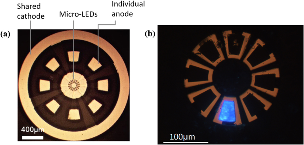
Figure 1.(a) Top-down micrograph image representation of a micro-LED array, showing the eight concentric and individually addressable pixels. (b) UV-C pixel in operation.
The light output power versus current (L-I) and current versus voltage (I-V) relationships were measured from representative pixels from each device. The I-V characteristics were measured using a Yokogawa GS610 source measure unit, and the L-I characteristics were measured by placing the pixels in close proximity to a calibrated Thorlabs S120VC power meter head. The results are shown in Fig. 2.
![]()
Figure 2.
The maximum output powers per pixel are approximately 0.48, 0.14, and 1.32 mW for the UV-C, UV-B, and UV-A devices, respectively. The most efficient device was the UV-A, which was expected, as this material technology is the most mature, and issues such as defects are minimized. The relatively low output power of the UV-B device may be attributed to the relative lack of development of material at these wavelengths, as there is currently no high-volume application for LEDs emitting in this range [18].
The forward voltages at 10 mA were 18.4, 22.0, and 4.4 V for the UV-C, UV-B, and UV-A devices, respectively. The higher turn-on voltages for the UV-B and UV-C devices can be attributed to the poor electrical conductivity of AlGaN layers, resulting in inferior carrier injection [18] and difficulties in creating low-resistance Ohmic contacts at higher Al mole fractions. These are prevalent issues in DUV material, and devices with higher turn-on voltages also being reported in the literature [5,19].
The EL spectra of the devices as a function of current were measured using a spectrometer and fiber optic (Avantes Avaspec-20482 spectrometer and Ocean Optics QP600-2-SR-BX fiber) (see Fig. 3). The peak wavelengths for each device were measured to be 281.7, 316.5, and 373.4 nm, respectively, when operating at 10 mA.
![]()
Figure 3.EL spectra of the three devices at 10 mA.
The spectra of the devices demonstrated different redshifts with the increasing current. This suggests heating effects were a more prominent issue in the UV-C device, which demonstrated a shift in the peak wavelength of 3.5 nm (from 281.7 to 285.2 nm) with increasing current from 0 to 30 mA. The shift is not as prominent in the other devices, with shifts of 1.2 nm being recorded for the UV-B over a current range of 0–12 mA and 1.16 nm being recorded in the UV-A devices, over the same range of current as the UV-C device. The measured spectra helped inform what filters and mirrors would be used in the WDM setup, which will be discussed in Section 3. It was noted that there was spectral overlap between the UV-C and UV-B devices, which could result in a degree of crosstalk between these WDM channels.
Finally, the frequency responses of the devices were measured using an avalanche photodiode (APD, Hamamatsu C5668 8867) with a bandwidth range of 100 kHz to 1 GHz, following a similar procedure, as outlined in our previous work [16]. Values for each device’s
Conventionally, when plotted on a logarithmic frequency scale, the frequency response of an LED should appear flat at low frequencies before gradually rolling off above a certain cut-off frequency. The
![]()
Figure 4.Frequency response of the UV-C μLED measured at 20 mA (black). The response at 1 MHz (indicated by the blue horizontal dotted line) is used as the low-frequency reference point to estimate the E-E
Our approach was to arbitrarily set the response at 1 MHz as the low-frequency reference and define the μLED bandwidth as the frequency at which the response declined to
![]()
Figure 5.Electrical-to-electrical bandwidth response versus current for the respective wavelengths.
The corresponding E-E bandwidths were found to be 960, 780, and 140 MHz, respectively. It is worth noting that the APD bandwidth (1 GHz) is close to that of the UV-B and -C μLEDs and, as a consequence, may have affected the estimated bandwidths. The further development of high-bandwidth UV/DUV sensitive APDs is urgently needed to facilitate the full measurement of μLED devices such as those reported here. Compared with their UV-A counterparts, the high modulation bandwidths and lower output power of the UV-B and -C devices may be attributed to higher defect densities and thus increased nonradiative recombination at shorter wavelengths. This would lead to lower output power and higher bandwidth via a reduced carrier recombination lifetime. We speculate that the saturation and decrease of the bandwidth as seen in the UV-B and UV-C, respectively, may be attributed to device heating and thermally mediated effects such as carrier overflow reducing the carrier density in the quantum wells, thus increasing the average carrier lifetime and reducing the bandwidth [20].
3. WDM EXPERIMENTAL SETUP
The WDM optical setup consists of the three UV μLED arrays and two long-pass dichroic mirrors with cut-on wavelengths of 355 nm (Semrock Di01-R355-
![]()
Figure 6.Spectra (red curves) of the dichroic mirrors used in the setup, and the spectra (blue data points) of the devices with each device operated at 10 mA.
![]()
Figure 7.Schematic diagram of the optical and electrical setup used for the WDM transmission experiments.
The emission from each μLED array was focused using a separate 2 in. diameter lens [Edmund Eptics 84340, focal length 40 mm for the UV-C and UV-B μLEDs, Thorlabs ACL50832U-A lens (
A MATLAB code was used to generate the DC-biased optical (DCO)-OFDM data similar to our previous work [16,21,22]. This code allowed for the evaluation and control of the setup’s performance, such as the peak-to-peak voltage, OFDM signal clipping, modulation bandwidth, number of subcarriers, cyclic prefix (CP) length, and the target bit error rate (BER) for adaptive bit and energy loading algorithm, which determined the final data rates achieved. Before transmitting the OFDM signal, a sinusoidal waveform was used to find an appropriate bias point with suitable peak-to-peak voltage and avoid any severe nonlinear distortion or saturation. After analyzing the performance, the following parameters were used: CP length of 20, normalized clipping level set to 3.2 of the signal standard deviation, corresponding PAPR of 10.1 dB, an FFT size of 2048, and a training length of 1504 QAM OFDM frames.
Next, a channel and signal-to-noise ratio (SNR) estimation procedure is executed, where 4QAM symbols are supplied to all subcarriers as the pilot signals. After an FFT (fast Fourier transform) operation, the detected symbols were compared with the original pilot symbols to estimate the channel gain and SNR for each subcarrier. The SNR information enables the use of an adaptive bit and energy loading algorithm [12], which selects the most suitable QAM constellation and transmission power for each subcarrier so that the eventual achieved BER will converge to a predefined threshold, thus maximizing the achievable data rate.
Next, the payload OFDM signal is transmitted. The QAM constellation and power control on each subcarrier are defined based on the adaptive bit and energy loading result. On the receiver side, the detected frequency-domain symbols are equalized using the estimated channel. Finally, the equalized symbols are decoded and compared with the original binary bits for BER calculation. The BER target used here is
In the WDM experiment, one μLED at a time was modulated with an OFDM signal, while the code simultaneously generated interfering signals in the other two μLED channels in order to simulate a real-world system with multiple parallel data streams. Furthermore, three amplifiers (one SFHS126A and two Minicircuits FL-1000LN+ amplifiers) were connected between the AWG and the bias TEE to amplify the RF signal and increase the signal modulation depth. The SFHS126A amplifier, with a gain of 29 dB, was connected to the μLED sending the desired OFDM signal. The receiver was situated 0.5 m from the transmitter. According to Ref. [23], the absorption and scattering coefficients at these wavelengths are on the order of
4. EXPERIMENTAL RESULTS
Before carrying out the main WDM experiment, the effect of the optical setup on the performance of the individual devices was examined. The performance of individual channels was evaluated where only one channel was operating at a time, and the performance was compared with and without a filter in front of the receiver. When filters were applied, a decrease in the SNR of each channel was observed due to optical losses from the filters. The decrease in SNR translated to an increase in the BER and thus a decrease of the maximum data rate.
![]()
Figure 8.(a) Comparison of BER when filters are applied to single pixels. (b) SNR of the devices in the WDM setup. (c) BER of three devices in the WDM setup. The dashed horizontal line in (a) and (c) corresponds to a BER of
M-QAM constellation diagrams from each WDM channel are shown in Fig. 9. As shown, the largest constellation sizes used were 32, 16, and 16 for the UV-C, -B, and -A channels, respectively, with corresponding BERs of
![]()
Figure 9.Maximum
The maximum data rates recorded were 4.17, 3.02, and 3.13 Gbps for the UV-C, -B, and -A devices, respectively, as can be seen in Fig. 8(c). The data rates per channel are also given in Table 1, at a BER of approximately
The performance of the devices behaved as expected based on the characterization measurements, with the UV-B showing the lowest maximum data rate. As shown in Fig. 2, the UV-B device emits the lowest output power among the three devices shown here. A small fraction of this output power is also lost when combining the three devices’ emission together for WDM, due to the less than 100% transmission of the “Alluxa” mirror, as shown in Fig. 6. It also has lower bandwidth than the UV-C device. These factors all contribute to the comparatively low data rate achieved by the UV-B device, even though this device had a higher bandwidth than the UV-A device.
When comparing the BER of the single pixels operating individually with the WDM values, the UV-C device produces similar results in both the WDM and the single device configuration. This can be attributed to the fact that the UV-C experienced the least crosstalk, as the filters and mirrors removed the unwanted light from the UV-B and -A devices. Conversely, the UV-B and UV-A channels show a marked improvement when only one pixel is on. This is due to the spectral overlap resulting in interference from adjacent channels affecting them, which is especially clear in the UV-A channel. The average received powers were estimated using a calibrated optical power meter to be 0.25, 0.03, and 0.10 mW for the UV-A, -B, and -C, respectively. However, due to the difference in active area between the power meter sensor and APD (9 and 0.5 mm diameter, respectively), the actual average received powers are likely to be significantly lower than this.
To the best of our knowledge, the highest optical wireless data rate reported for a single DUV μLED was 2 Gbps obtained by Zhu
5. CONCLUSION
This work has demonstrated a three-channel UV-WDM setup using μLEDs with peak emission in the UV-A (375 nm), UV-B (317 nm), and UV-C (285 nm) regions of the ultraviolet spectrum. Using OFDM and QAM modulation schemes and forward error correction, we achieved data rates of 4.17, 3.02, and 3.13 Gbps from the UV-C, UV-B, and UV-A devices, respectively. The data rates from each individual channel, taken in isolation, represent, to our best knowledge, the highest rates yet reported for a UV μLED and, added together, result in a combined data rate of 10.32 Gbps, demonstrating an LED-based UV optical wireless link exceeding 10 Gbps.
Acknowledgment
Acknowledgment. We acknowledge Zhixin Semiconductor Co., Ltd. for the LED wafer material. We acknowledge Fraunhofer UK Research Ltd. for DM’s PhD studentship funding. All authors declare there are no competing financial interests involved in this work.
References
[1] H. Haas. LiFi is a paradigm-shifting 5G technology. Rev. Phys., 3, 26-31(2017).
[2] D. O’Brien, S. Rajbhandari, H. Chun. Transmitter and receiver technologies for optical wireless. Philos. Trans. R. Soc. A, 378, 20190182(2020).
[3] R. J. Drost, B. M. Sadler. Survey of ultraviolet non-line-of-sight communications. Semicond. Sci. Technol., 29, 084006(2014).
[4] G. Chen, Z. Xu, B. M. Sadler. Experimental demonstration of ultraviolet pulse broadening in short-range non-line-of-sight communication channels. Opt. Express, 18, 10500-10509(2010).
[5] A. Vavoulas, H. G. Sandalidis, N. D. Chatzidiamantis, Z. Xu, G. K. Karagiannidis. A survey on ultraviolet C-band (UV-C) communications. Commun. Surveys Tuts., 21, 2111-2133(2019).
[6] Z. Xu, B. M. Sadler. Ultraviolet communications: potential and state-of-the-art. IEEE Commun. Mag., 46, 67-73(2008).
[7] Z. Zhang, M. Kushimoto, T. Sakai, N. Sugiyama, L. Schowalter, C. Sasaoka, H. Amano. A 271.8 nm deep-ultraviolet laser diode for room temperature operation. Appl. Phys. Express, 12, 8-12(2019).
[8] H. S. Wasisto, J. D. Prades, J. Gülink, A. Waag. Beyond solid-state lighting: miniaturization, hybrid integration, and applications of GaN nano-and micro-LEDs. Appl. Phys. Rev., 6, 041315(2019).
[9] G.-R. Lin, H.-C. Kuo, C.-H. Cheng, Y.-C. Wu, Y.-M. Huang, F.-J. Liou, Y.-C. Lee. Ultrafast 2 × 2 green micro-LED array for optical wireless communication beyond 5 Gbit/s. Photon. Res., 9, 2077-2087(2021).
[10] D. Peng, K. Zhang, Z. Liu. Design and fabrication of fine-pitch pixelated-addressed micro-LED arrays on printed circuit board for display and communication applications. IEEE J. Electron Devices Soc., 5, 90-94(2017).
[11] R. P. Green, J. J. D. McKendry, D. Massoubre, E. Gu, M. D. Dawson, A. E. Kelly. Modulation bandwidth studies of recombination processes in blue and green InGaN quantum well micro-light-emitting diodes. Appl. Phys. Lett., 102, 091103(2013).
[12] M. S. Islim, R. X. Ferreira, X. He, E. Xie, S. Videv, S. Viola, S. Watson, N. Bamiedakis, R. V. Penty, I. H. White, A. E. Kelly, E. Gu, H. Haas, M. D. Dawson. Towards 10 Gb/s orthogonal frequency division multiplexing-based visible light communication using a GaN violet micro-LED. Photon. Res., 5, A35-A43(2017).
[13] S. Zhu, P. Qiu, Z. Qian, X. Shan, Z. Wang, K. Jiang, X. Sun, X. Cui, G. Zhang, D. Li, P. Tian. 2 Gbps free-space ultraviolet-C communication based on a high-bandwidth micro-LED achieved with pre-equalization. Opt. Lett., 46, 2147-2150(2021).
[14] C. Jeon, H. W. Choi, E. Gu, M. D. Dawson, S. Member. High-density matrix-addressable AlInGaN-based 368-nm microarray light-emitting diodes. IEEE Photon. Technol. Lett., 16, 2421-2423(2004).
[15] B. Guilhabert, D. Massoubre, E. Richardson, J. J. D. McKendry, G. Valentine, R. K. Henderson, I. M. Watson, E. Gu, M. D. Dawson. Sub-micron lithography using InGaN micro-LEDs: mask-free fabrication of LED arrays. IEEE Photon. Technol. Lett., 24, 2221-2224(2012).
[16] X. He, E. Xie, M. S. Islim, A. A. Purwita, J. J. D. McKendry, E. Gu, H. Haas, M. D. Dawson. 1 Gbps free-space deep-ultraviolet communications based on III-nitride micro-LEDs emitting at 262 nm. Photon. Res., 7, B41-B47(2019).
[17] R. X. G. Ferreira, E. Xie, J. J. D. McKendry, S. Rajbhandari, H. Chun, G. Faulkner, S. Watson, A. E. Kelly, E. Gu. High bandwidth GaN-based micro-LEDs for multi-Gb/s visible light communications. IEEE Photon. Technol. Lett., 28, 2023-2026(2016).
[18] H. Amano, R. Collazo, C. D. Santi, S. Einfeldt, M. Funato, J. Glaab, S. Hagedorn, A. Hirano, H. Hirayama, R. Ishii, Y. Kashima, R. Kirste, M. Kneissl, R. W. Martin, F. Mehnke, M. Meneghini, A. Ougazzaden, P. Parbrook, S. Rajan, P. Reddy. The 2020 UV emitter roadmap. J. Phys. D, 53, 503001(2020).
[19] M. Kneissl, T. Y. Seong, J. Han, H. Amano. The emergence and prospects of deep-ultraviolet light-emitting diode technologies. Nat. Photonics, 13, 233-244(2019).
[20] S. W. H. Chen, Y.-M. Huang, Y.-H. Chang, Y. Lin, F.-J. Liou, Y.-C. Hsu, J. Song, J. Choi, C.-W. Chow, C.-C. Lin, R.-H. Horng, Z. Chen, J. Han, T. Wu, H.-C. Kuo. High-bandwidth green semipolar (20-21) InGaN/GaN micro light-emitting diodes for visible light communication. ACS Photon., 7, 2228-2235(2020).
[21] D. Tsonev, H. Chun, S. Rajbhandari, J. J. D. McKendry, S. Videv, E. Gu, M. Haji. A 3-Gb/s single-LED OFDM-based wireless VLC link using a gallium nitride μLED. IEEE Photon. Technol. Lett., 26, 637-640(2014).
[22] J. F. C. Carreira, E. Xie, R. Bian, J. Herrnsdorf, H. Haas, E. Gu, M. J. Strain, M. D. Dawson. Gigabit per second visible light communication based on AlGaInP red micro-LED micro-transfer printed onto diamond and glass. Opt. Express, 28, 12149-12156(2020).
[23] H. Ding, G. Chen, A. K. Majumdar, B. M. Sadler, Z. Xu. “Modeling of non-line-of-sight ultraviolet scattering channels for communication. IEEE J. Sel. Areas Commun., 27, 1535-1544(2009).
[24] X. Liu, Z. Wei, M. Li, L. Wang, Z. Liu, C. Yu, L. Wang, Y. Luo, H. Y. Fu. Experimental investigation of 16.6 Gbps SDM-WDM visible light communication based on a neural network receiver and tricolor mini-LEDs. Opt. Lett., 46, 2888-2891(2021).
[25] G. Cossu, A. M. Khalid, P. Choudhury, R. Corsini, E. Ciaramella. 3.4 Gbit/s visible optical wireless transmission based on RGB LED. Optics Express, 20, B501-B506(2012).
[26] X. Sun, Z. Zhang, A. Chaaban, T. K. Ng, C. Shen, R. Chen, J. Yan, H. Sun, X. Li, J. Wang, J. Li, M.-S. Alouini, B. S. Ooi. 71-Mbit/s ultraviolet-B LED communication link based on 8-QAM-OFDM modulation. Opt. Express, 25, 23267-23274(2017).


Set citation alerts for the article
Please enter your email address

© Copyright 2018-2021 | Chinese Laser Press. All Rights Reserved 沪ICP备15018463号-20