• Photonics Research
  • Vol. 10, Issue 2, 535 (2022)
Weiqiang Xie1、2、†, Chao Xiang1、†, Lin Chang1, Warren Jin1, Jonathan Peters1, and John E. Bowers1、*
Author Affiliations
  • 1Department of Electrical and Computer Engineering, University of California, Santa Barbara, Santa Barbara, California 93106, USA
  • 2Current address: Department of Electronic Engineering, Shanghai Jiao Tong University, Shanghai 200240, China
  • show less
    DOI: 10.1364/PRJ.446898 Cite this Article Set citation alerts
    Weiqiang Xie, Chao Xiang, Lin Chang, Warren Jin, Jonathan Peters, John E. Bowers. Silicon-integrated nonlinear III-V photonics[J]. Photonics Research, 2022, 10(2): 535 Copy Citation Text show less
    AlGaAs-Si heterogeneous nonlinear photonics integration. (a) Schematic of the AlGaAs-Si integration architecture. (b) Simulated TE0 mode profile of AlGaAs waveguide on SOI with spacer oxide and air trench. (c) Photograph of the fabricated chip containing 100G FSR devices diced from a 100 mm diameter SOI wafer. (d) False-colored SEM image of a fabricated suspended AlGaAs microring. (e) Optical microscope image of the Si-AlGaAs taper.
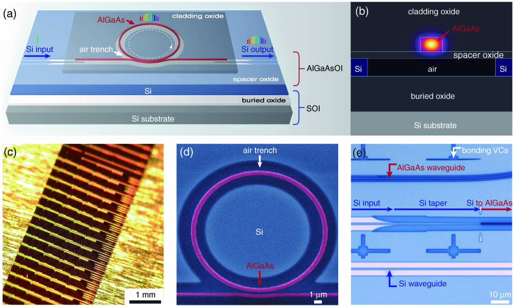
    Fig. 1. AlGaAs-Si heterogeneous nonlinear photonics integration. (a) Schematic of the AlGaAs-Si integration architecture. (b) Simulated TE0 mode profile of AlGaAs waveguide on SOI with spacer oxide and air trench. (c) Photograph of the fabricated chip containing 100G FSR devices diced from a 100 mm diameter SOI wafer. (d) False-colored SEM image of a fabricated suspended AlGaAs microring. (e) Optical microscope image of the Si-AlGaAs taper.
    Simplified schematic of the device fabrication process. (a) Device process overview and cross sectional SOI wafer and AlGaAs epi layer details. (b) Cross sectional schematics of the full process including: Si waveguide formation, Si taper/air trench/VC formation, AlGaAs bonding, GaAs substrate removal, AlGaAs taper/ring formation, and SiO2 cladding deposition.
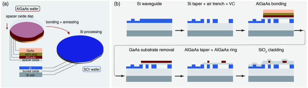
    Fig. 2. Simplified schematic of the device fabrication process. (a) Device process overview and cross sectional SOI wafer and AlGaAs epi layer details. (b) Cross sectional schematics of the full process including: Si waveguide formation, Si taper/air trench/VC formation, AlGaAs bonding, GaAs substrate removal, AlGaAs taper/ring formation, and SiO2 cladding deposition.
    Characterization of AlGaAs-Si integrated devices. (a) Measured transmission spectra of waveguides with pairs of Si-AlGaAs tapers together with the transmission of a Si waveguide for reference. Inset: simulated transmission of the Si-AlGaAs taper under different lateral misalignments. (b) Measured transmission at 1550 nm versus number of Si-AlGaAs tapers. (c) Dispersion of the TE0 mode as a function of relative mode number for a 0.5 THz FSR microring. Transmission spectra and measured intrinsic Q0 factors of resonances at 1532.86 nm and 1521.72 nm for (d) microring with a radius of 12 μm and width of 650 nm and (e) microring with a radius of 143 μm and width of 650 nm, respectively.
    Fig. 3. Characterization of AlGaAs-Si integrated devices. (a) Measured transmission spectra of waveguides with pairs of Si-AlGaAs tapers together with the transmission of a Si waveguide for reference. Inset: simulated transmission of the Si-AlGaAs taper under different lateral misalignments. (b) Measured transmission at 1550 nm versus number of Si-AlGaAs tapers. (c) Dispersion of the TE0 mode as a function of relative mode number for a 0.5 THz FSR microring. Transmission spectra and measured intrinsic Q0 factors of resonances at 1532.86 nm and 1521.72 nm for (d) microring with a radius of 12 μm and width of 650 nm and (e) microring with a radius of 143 μm and width of 650 nm, respectively.
    Frequency comb spectra measured from Si waveguide edge coupler for two AlGaAs microrings: 1 THz ring at pump powers of (a) 0.25 mW, (b) 0.4 mW, and (c) 3 mW; (d) 90 GHz ring at pump power of 15.8 mW. Inset in (d): close-up of the comb spectrum in a selected wavelength range.
    Fig. 4. Frequency comb spectra measured from Si waveguide edge coupler for two AlGaAs microrings: 1 THz ring at pump powers of (a) 0.25 mW, (b) 0.4 mW, and (c) 3 mW; (d) 90 GHz ring at pump power of 15.8 mW. Inset in (d): close-up of the comb spectrum in a selected wavelength range.
    Weiqiang Xie, Chao Xiang, Lin Chang, Warren Jin, Jonathan Peters, John E. Bowers. Silicon-integrated nonlinear III-V photonics[J]. Photonics Research, 2022, 10(2): 535
    Download Citation