
Weiqiang Xie, Chao Xiang, Lin Chang, Warren Jin, Jonathan Peters, John E. Bowers, "Silicon-integrated nonlinear III-V photonics," Photonics Res. 10, 535 (2022)
- Photonics Research
- Vol. 10, Issue 2, 535 (2022)
Abstract
1. INTRODUCTION
Silicon photonics based on silicon-on-insulator (SOI) substrates has been rapidly growing over the past two decades, providing various on-chip passive/active photonic functionalities (waveguide-based passive components, modulators, photodetectors, etc.) by taking advantage of mature planar CMOS technology, leading to the development of Si photonic integrated circuits (PICs) [1–4]. Moreover, III–V-on-Si (III-V/Si) heterogeneous integration techniques have been developed to address the laser source issue for Si photonics and have now been adopted in scalable state-of-the-art CMOS-compatible processes [5]. Today, Si photonics is playing a leading role in the community of integrated photonics and has found applications in a large number of areas including optical interconnects [6,7], telecommunications [8], computing [9], and so on [10]. Meanwhile, significant progress spanning the last decade on integrated nonlinear photonics has emerged as a new paradigm for both nonlinear optics research and applications. An intriguing offering of integrated nonlinear photonics is its capability of generating new classes of coherent, ultra-broadband light sources (i.e., microcombs) in nonlinear waveguides [11,12], which is not attainable from linear photonics systems. Microcombs have triggered widespread use of chip-scale nonlinear devices in applications [13] including ultrahigh-capacity coherent telecommunications [14,15], optical frequency synthesis [16], optical atomic clocks [17], quantum optics [18], etc. In the past few years, significant technological advances have enabled ultralow-loss nonlinear waveguides and ultrahigh-quality-factor (
Therefore, it is naturally desired to embed nonlinear functionalities in relatively mature Si PICs for complete chip-scale nonlinear photonics with the ability of direct signal generation and processing. However, Si has inherent disadvantages regarding many nonlinear applications, such as its small-bandgap-induced strong two-photon absorption (TPA) and related free-carrier losses at telecom wavelengths and insignificant
Here, we further extend the integration of AlGaAs nonlinear photonics onto an SOI substrate with the goal of bridging “the silicon of nonlinear optical materials” and Si PICs. To achieve this goal, we propose a general heterogeneous architecture to combine the two types of PICs with fabrication compatibility and integration scalability. We demonstrate low-loss AlGaAs-on-SOI waveguides and microresonators with
Sign up for Photonics Research TOC. Get the latest issue of Photonics Research delivered right to you!Sign up now
2. DESIGN AND FABRICATION
Figure 1(a) depicts the proposed device configuration whereby light in the bottom SOI layer is coupled to the top AlGaAs layer and vice versa via evanescent coupling aided by a pair of inverse tapers of Si and AlGaAs waveguides. The two device layers are spaced by an oxide layer of certain thickness (200 nm in current case). In practice, this structure can be realized by low-temperature (typically
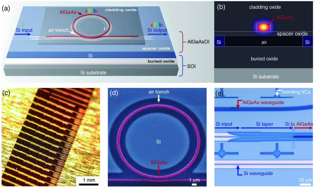
Figure 1.AlGaAs-Si heterogeneous nonlinear photonics integration. (a) Schematic of the AlGaAs-Si integration architecture. (b) Simulated TE0 mode profile of AlGaAs waveguide on SOI with spacer oxide and air trench. (c) Photograph of the fabricated chip containing 100G FSR devices diced from a 100 mm diameter SOI wafer. (d) False-colored SEM image of a fabricated suspended AlGaAs microring. (e) Optical microscope image of the Si-AlGaAs taper.
In Fig. 2, we present the simplified fabrication process. The overall fabrication consists of three major steps: Si waveguide patterning on the SOI wafer, AlGaAs epi wafer bonding, and AlGaAs waveguide patterning [Fig. 2(a)]. The details of the process flow are shown in Fig. 2(b). For the entire process, a 248 nm deep ultraviolet (DUV) stepper was used for photolithography, which is well suited for scalable integration and volume fabrication. The fabrication started with the deposition of 200 nm oxide on a 100-mm-diameter SOI wafer using plasma-enhanced chemical vapor deposition (PECVD). The oxide layer was then patterned and dry etched with chemistries of
![]()
Figure 2.Simplified schematic of the device fabrication process. (a) Device process overview and cross sectional SOI wafer and AlGaAs epi layer details. (b) Cross sectional schematics of the full process including: Si waveguide formation, Si taper/air trench/VC formation, AlGaAs bonding, GaAs substrate removal, AlGaAs taper/ring formation, and
3. DEVICE CHARACTERIZATION
We first characterized the transmission spectral response of our devices. TE polarized light from a tunable laser was coupled into one Si waveguide through a lensed fiber, and the output was collected by another lensed fiber from the other Si waveguide edge coupler, as denoted in Fig. 1(a). The transmitted power was detected with a high-speed photodetector, and the response was recorded using an oscilloscope. The spectral resolution of our measurement is 0.01 pm. The input power can be further adjusted with a variable optical attenuator. Figure 3(a) shows the transmission spectra of several waveguides with the same input/output Si edge couplers connected by a series of Si-AlGaAs tapers (two, four, and six tapers) and a pure Si waveguide (zero tapers) for reference. We extracted the taper loss at the wavelength of 1550 nm with a linear fit of the transmission as a function of the number of tapers in dB scale and show the results in Fig. 3(b), indicating a Si-AlGaAs taper loss of 0.87 dB, e.g., a coupling efficiency of 82%. For comparison, we also show the simulated taper transmission in the inset of Fig. 3(a) with a theoretical coupling efficiency of 95% at 1550 nm. Additionally, the effect of lateral misalignment between the tapers is also simulated, indicating a tolerance of at least 100 nm for
![]()
Figure 3.Characterization of AlGaAs-Si integrated devices. (a) Measured transmission spectra of waveguides with pairs of Si-AlGaAs tapers together with the transmission of a Si waveguide for reference. Inset: simulated transmission of the Si-AlGaAs taper under different lateral misalignments. (b) Measured transmission at 1550 nm versus number of Si-AlGaAs tapers. (c) Dispersion of the TE0 mode as a function of relative mode number for a 0.5 THz FSR microring. Transmission spectra and measured intrinsic
The waveguide dispersion and the
To further highlight the capability of efficient nonlinear applications in the developed AlGaAs-SOI platform, we performed a frequency comb generation experiment, in which the pump laser was injected to the AlGaAs ring through the input Si waveguide edge coupler, and the comb spectrum was collected from the output Si waveguide edge coupler. For the ring with an FSR of 1 THz, we pumped a resonance at
![]()
Figure 4.Frequency comb spectra measured from Si waveguide edge coupler for two AlGaAs microrings: 1 THz ring at pump powers of (a) 0.25 mW, (b) 0.4 mW, and (c) 3 mW; (d) 90 GHz ring at pump power of 15.8 mW. Inset in (d): close-up of the comb spectrum in a selected wavelength range.
Additionally, we estimated the comb threshold power theoretically, using the expression [60]
4. CONCLUSION
In summary, we demonstrated a general architecture for efficient integration between two important integrated photonics platforms, i.e., a mature SOI waveguide platform and an emerging nonlinear III-V platform. We showcase efficient
Acknowledgment
Acknowledgment. We thank Justin C. Norman, Chenlei Li, and Joel Guo for helpful discussions.
References
[1] M. Lipson. Guiding, modulating, and emitting light on silicon-challenges and opportunities. J. Lightwave Technol., 23, 4222-4238(2005).
[2] R. Soref. The past, present, and future of silicon photonics. IEEE J. Sel. Top. Quantum Electron., 12, 1678-1687(2006).
[3] W. Bogaerts, R. Baets, P. Dumon, V. Wiaux, S. Beckx, D. Taillaert, B. Luyssaert, J. Van Campenhout, P. Bienstman, D. Van Thourhout. Nanophotonic waveguides in silicon-on-insulator fabricated with CMOS technology. J. Lightwave Technol., 23, 401-412(2005).
[4] A. E.-J. Lim, J. Song, Q. Fang, C. Li, X. Tu, N. Duan, K. K. Chen, R. P.-C. Tern, T.-Y. Liow. Review of silicon photonics foundry efforts. IEEE J. Sel. Top. Quantum Electron., 20, 405-416(2013).
[5] R. Jones, P. Doussiere, J. B. Driscoll, W. Lin, H. Yu, Y. Akulova, T. Komljenovic, J. E. Bowers. Heterogeneously integrated InP/silicon photonics: fabricating fully functional transceivers. IEEE Nanotechnol. Mag., 13, 17-26(2019).
[6] Y. Arakawa, T. Nakamura, Y. Urino, T. Fujita. Silicon photonics for next generation system integration platform. IEEE Commun. Mag., 51, 72-77(2013).
[7] D. Dai, J. E. Bowers. Silicon-based on-chip multiplexing technologies and devices for peta-bit optical interconnects. Nanophotonics, 3, 283-311(2014).
[8] C. R. Doerr. Silicon photonic integration in telecommunications. Front. Phys., 3, 37(2015).
[9] W. Bogaerts, D. Pérez, J. Capmany, D. A. Miller, J. Poon, D. Englund, F. Morichetti, A. Melloni. Programmable photonic circuits. Nature, 586, 207-216(2020).
[10] N. Margalit, C. Xiang, S. M. Bowers, A. Bjorlin, R. Blum, J. E. Bowers. Perspective on the future of silicon photonics and electronics. Appl. Phys. Lett., 118, 220501(2021).
[11] M. A. Foster, A. C. Turner, M. Lipson, A. L. Gaeta. Nonlinear optics in photonic nanowires. Opt. Express, 16, 1300-1320(2008).
[12] A. L. Gaeta, M. Lipson, T. J. Kippenberg. Photonic-chip-based frequency combs. Nat. Photonics, 13, 158-169(2019).
[13] T. J. Kippenberg, A. L. Gaeta, M. Lipson, M. L. Gorodetsky. Dissipative Kerr solitons in optical microresonators. Science, 361, eaan8083(2018).
[14] P. Marin-Palomo, J. N. Kemal, M. Karpov, A. Kordts, J. Pfeifle, M. H. P. Pfeiffer, P. Trocha, S. Wolf, V. Brasch, M. H. Anderson, R. Rosenberger, K. Vijayan, W. Freude, T. J. Kippenberg, C. Koos. Microresonator-based solitons for massively parallel coherent optical communications. Nature, 546, 274-279(2017).
[15] H. Hu, F. Da Ros, M. Pu. Single-source chip-based frequency comb enabling extreme parallel data transmission. Nat. Photonics, 12, 469-473(2018).
[16] D. T. Spencer, T. Drake, T. C. Briles. An optical-frequency synthesizer using integrated photonics. Nature, 557, 81-85(2018).
[17] D. T. Spencer, T. Drake, T. C. Briles, J. Stone, L. C. Sinclair, C. Fredrick, Q. Li, D. Westly, B. R. Ilic, A. Bluestone, N. Volet, T. Komljenovic, L. Chang, S. H. Lee, D. Y. Oh, M.-G. Suh, K. Y. Yang, M. H. P. Pfeiffer, T. J. Kippenberg, E. Norberg, L. Theogarajan, K. Vahala, N. R. Newbury, K. Srinivasan, J. E. Bowers, S. A. Diddams, S. B. Papp. Architecture for the photonic integration of an optical atomic clock. Optica, 6, 680-685(2019).
[18] M. A. Guidry, D. M. Lukin, K. Y. Yang, R. Trivedi, J. Vučković. Quantum optics of soliton microcombs. Nat. Photonics, 16, 52-58(2022).
[19] X. Ji, F. A. S. Barbosa, S. P. Roberts, A. Dutt, J. Cardenas, Y. Okawachi, A. Bryant, A. L. Gaeta, M. Lipson. Ultra-low-loss on-chip resonators with sub-milliwatt parametric oscillation threshold. Optica, 4, 619-624(2017).
[20] M. Zhang, C. Wang, R. Cheng, A. Shams-Ansari, M. Lončar. Monolithic ultra-high-
[21] W. Xie, L. Chang, H. Shu, J. C. Norman, J. D. Peters, X. Wang, J. E. Bowers. Ultrahigh-
[22] J. Liu, G. Huang, R. N. Wang, J. He, A. S. Raja, T. Liu, N. J. Engelsen, T. J. Kippenberg. High-yield, wafer-scale fabrication of ultralow-loss, dispersion-engineered silicon nitride photonic circuits. Nat. Commun., 12, 2236(2021).
[23] M. W. Puckett, K. Liu, N. Chauhan, Q. Zhao, N. Jin, H. Cheng, J. Wu, R. O. Behunin, P. T. Rakich, K. D. Nelson, D. J. Blumenthal. 422 million intrinsic quality factor planar integrated all-waveguide resonator with sub-MHz linewidth. Nat. Commun., 12, 934(2021).
[24] J. Liu, A. S. Raja, M. Karpov, B. Ghadiani, M. H. P. Pfeiffer, B. Du, N. J. Engelsen, H. Guo, M. Zervas, T. J. Kippenberg. Ultralow-power chip-based soliton microcombs for photonic integration. Optica, 5, 1347-1353(2018).
[25] B. Stern, X. Ji, Y. Okawachi, A. L. Gaeta, M. Lipson. Battery-operated integrated frequency comb generator. Nature, 562, 401-405(2018).
[26] A. S. Raja, A. S. Voloshin, H. Guo, S. E. Agafonova, J. Liu, A. S. Gorodnitskiy, M. Karpov, N. G. Pavlov, E. Lucas, R. R. Galiev, A. E. Shitikov, J. D. Jost, M. L. Gorodetsky, T. J. Kippenberg. Electrically pumped photonic integrated soliton microcomb. Nat. Commun., 10, 680(2019).
[27] B. Shen, L. Chang, J. Liu, H. Wang, Q.-F. Yang, C. Xiang, R. N. Wang, J. He, T. Liu, W. Xie, J. Guo, D. Kinghorn, L. Wu, Q.-X. Ji, T. J. Kippenberg, K. Vahala, J. E. Bowers. Integrated turnkey soliton microcombs. Nature, 582, 365-369(2020).
[28] W. Jin, Q.-F. Yang, L. Chang, B. Shen, H. Wang, M. A. Leal, L. Wu, M. Gao, A. Feshali, M. Paniccia, K. J. Vahala, J. E. Bowers. Hertz-linewidth semiconductor lasers using CMOS-ready ultra-high-
[29] C. Xiang, J. Liu, J. Guo, L. Chang, R. N. Wang, W. Weng, J. Peters, W. Xie, Z. Zhang, J. Riemensberger, J. Selvidge, T. J. Kippenberg, J. E. Bowers. Laser soliton microcombs heterogeneously integrated on silicon. Science, 373, 99-103(2021).
[30] M. A. Foster, A. C. Turner, J. E. Sharping, B. S. Schmidt, M. Lipson, A. L. Gaeta. Broad-band optical parametric gain on a silicon photonic chip. Nature, 441, 960-963(2006).
[31] J. Leuthold, C. Koos, W. Freude. Nonlinear silicon photonics. Nat. Photonics, 4, 535-544(2010).
[32] C. Xiang, W. Jin, J. Guo, C. Williams, A. M. Netherton, L. Chang, P. A. Morton, J. E. Bowers. Effects of nonlinear loss in high-
[33] D. J. Moss, R. Morandotti, A. L. Gaeta, M. Lipson. New CMOS-compatible platforms based on silicon nitride and hydex for nonlinear optics. Nat. Photonics, 7, 597-607(2013).
[34] B. J. Eggleton, B. Luther-Davies, K. Richardson. Chalcogenide photonics. Nat. Photonics, 5, 141-148(2011).
[35] C. Xiong, W. Pernice, K. K. Ryu, C. Schuck, K. Y. Fong, T. Palacios, H. X. Tang. Integrated GaN photonic circuits on silicon (100) for second harmonic generation. Opt. Express, 19, 10462-10470(2011).
[36] C. Xiong, W. H. P. Pernice, X. Sun, C. Schuck, K. Y. Fong, H. X. Tang. Aluminum nitride as a new material for chip-scale optomechanics and nonlinear optics. New J. Phys., 14, 095014(2012).
[37] U. D. Dave, B. Kuyken, F. Leo, S.-P. Gorza, S. Combrie, A. De Rossi, F. Raineri, G. Roelkens. Nonlinear properties of dispersion engineered InGaP photonic wire waveguides in the telecommunication wavelength range. Opt. Express, 23, 4650-4657(2015).
[38] C. Wang, C. Langrock, A. Marandi, M. Jankowski, M. Zhang, B. Desiatov, M. M. Fejer, M. Lončar. Ultrahigh-efficiency wavelength conversion in nanophotonic periodically poled lithium niobate waveguides. Optica, 5, 1438-1441(2018).
[39] D. M. Lukin, C. Dory, M. A. Guidry, K. Y. Yang, S. D. Mishra, R. Trivedi, M. Radulaski, S. Sun, D. Vercruysse, G. H. Ahn, J. Vučković. 4H-silicon-carbide-on-insulator for integrated quantum and nonlinear photonics. Nat. Photonics, 14, 330-334(2020).
[40] D. J. Wilson, K. Schneider, S. Hönl, M. Anderson, Y. Baumgartner, L. Czornomaz, T. J. Kippenberg, P. Seidler. Integrated gallium phosphide nonlinear photonics. Nat. Photonics, 14, 57-62(2020).
[41] H. Jung, S.-P. Yu, D. R. Carlson, T. E. Drake, T. C. Briles, S. B. Papp. Tantala Kerr nonlinear integrated photonics. Optica, 8, 811-817(2021).
[42] M. Pu, L. Ottaviano, E. Semenova, K. Yvind. Efficient frequency comb generation in AlGaAs-on-insulator. Optica, 3, 823-826(2016).
[43] L. Chang, W. Xie, H. Shu, Q.-F. Yang, B. Shen, A. Boes, J. D. Peters, W. Jin, C. Xiang, S. Liu, G. Moille, S.-P. Yu, X. Wang, K. Srinivasan, S. B. Papp, K. Vahala, J. E. Bowers. Ultra-efficient frequency comb generation in AlGaAs-on-insulator microresonators. Nat. Communications, 11, 1331(2020).
[44] M. A. Afromowitz. Refractive index of Ga1-
[45] G. Stegeman, A. Villeneuve, J. Kang, J. Aitchison, C. Ironside, K. Al-Hemyari, C. Yang, C.-H. Lin, H.-H. Lin, G. Kennedy, R. S. Grant, W. Sibbett. AlGaAs below half bandgap: the silicon of nonlinear optical materials. Int. J. Nonlinear Opt. Phys., 3, 347-371(1994).
[46] J. S. Aitchison, D. Hutchings, J. Kang, G. Stegeman, A. Villeneuve. The nonlinear optical properties of AlGaAs at the half band gap. IEEE J. Quantum Electron., 33, 341-348(1997).
[47] S. Ho, C. Soccolich, M. Islam, W. Hobson, A. Levi, R. Slusher. Large nonlinear phase shifts in low-loss Al
[48] K. Dolgaleva, W. C. Ng, L. Qian, J. S. Aitchison. Compact highly-nonlinear AlGaAs waveguides for efficient wavelength conversion. Opt. Express, 19, 12440-12455(2011).
[49] J. J. Wathen, P. Apiratikul, C. J. Richardson, G. A. Porkolab, G. M. Carter, T. E. Murphy. Efficient continuous-wave four-wave mixing in bandgap-engineered AlGaAs waveguides. Opt. Lett., 39, 3161-3164(2014).
[50] J. McPhillimy, S. May, C. Klitis, B. Guilhabert, M. D. Dawson, M. Sorel, M. J. Strain. Transfer printing of AlGaAs-on-SOI microdisk resonators for selective mode coupling and low-power nonlinear processes. Opt. Lett., 45, 881-884(2020).
[51] H. El Dirani, C. Monat, S. Brision, N. Olivier, C. Jany, X. Letartre, M. Pu, P. D. Girouard, L. H. Frandsen, E. Semenova, L. K. Oxenløwe, K. Yvind, C. Sciancalepore. SiNOI and AlGaAs-on-SOI nonlinear circuits for continuum generation in Si photonics. Proc. SPIE, 10535, 1053508(2018).
[52] J. Chiles, N. Nader, E. J. Stanton, D. Herman, G. Moody, J. Zhu, J. C. Skehan, B. Guha, A. Kowligy, J. T. Gopinath, K. Srinivasan, S. A. Diddams, I. Coddington, N. R. Newbury, J. M. Shainline, S. W. Nam, R. P. Mirin. Multifunctional integrated photonics in the mid-infrared with suspended AlGaAs on silicon. Optica, 6, 1246-1254(2019).
[53] E. J. Stanton, L. Chang, W. Xie, A. Malik, J. Peters, J. Chiles, N. Nader, G. Navickaite, D. Sacchetto, M. Zervas, K. Srinivasan, J. E. Bowers, S. B. Papp, S. W. Nam, R. P. Mirin. On-chip polarization rotator for type I second harmonic generation. APL Photon., 4, 126105(2019).
[54] E. J. Stanton, J. Chiles, N. Nader, G. Moody, N. Volet, L. Chang, J. E. Bowers, S. W. Nam, R. P. Mirin. Efficient second harmonic generation in nanophotonic GaAs-on-insulator waveguides. Opt. Express, 28, 9521-9532(2020).
[55] B. Kuyken, M. Billet, F. Leo, K. Yvind, M. Pu. Octave-spanning coherent supercontinuum generation in an AlGaAs-on-insulator waveguide. Opt. Lett., 45, 603-606(2020).
[56] G. Moille, L. Chang, W. Xie, A. Rao, X. Lu, M. Davanco, J. E. Bowers, K. Srinivasan. Dissipative Kerr solitons in a III-V microresonator. Laser Photon. Rev., 14, 2000022(2020).
[57] H. Shu, B. Shen, L. Chang, W. Xie, J. Qin, M. Jin, X. Zhang, X. Wang, J. E. Bowers. Mode-locked dark-pulse Kerr combs in normal-dispersion AlGaAs-on-insulator microresonators. Conference on Lasers and Electro-Optics, STu2G.4(2021).
[58] T. J. Steiner, J. E. Castro, L. Chang, Q. Dang, W. Xie, J. Norman, J. E. Bowers, G. Moody. Ultrabright entangled-photon-pair generation from an AlGaAs-on-insulator microring resonator. PRX Quantum, 2, 010337(2021).
[59] S. Zhang, J. M. Silver, L. Del Bino, F. Copie, M. T. Woodley, G. N. Ghalanos, A. Ø. Svela, N. Moroney, P. Del’Haye. Sub-milliwatt-level microresonator solitons with extended access range using an auxiliary laser. Optica, 6, 206-212(2019).
[60] A. B. Matsko, A. A. Savchenkov, D. Strekalov, V. S. Ilchenko, L. Maleki. Optical hyperparametric oscillations in a whispering-gallery-mode resonator: threshold and phase diffusion. Phys. Rev. A, 71, 033804(2005).


Set citation alerts for the article
Please enter your email address

© Copyright 2018-2021 | Chinese Laser Press. All Rights Reserved 沪ICP备15018463号-20