• Chinese Optics Letters
  • Vol. 21, Issue 3, 032501 (2023)
Tiancai Wang1、2, Peng Cao1、2, Hongling Peng1、3、*, Chuanwang Xu1、2, Haizhi Song4, and Wanhua Zheng1、3、5、6、**
Author Affiliations
  • 1Laboratory of Solid-State Optoelectronics Information Technology, Institute of Semiconductors, Chinese Academy of Sciences, Beijing 100083, China
  • 2College of Electronic and Communication Engineering, University of Chinese Academy of Sciences, Beijing 100049, China
  • 3State Key Laboratory on Integrated Optoelectronics, Institute of Semiconductors, Chinese Academy of Sciences, Beijing 100083, China
  • 4Southwest Institute of Technology Physics, Chengdu 610041, China
  • 5Center of Materials Science and Optoelectronics Engineering, University of Chinese Academy of Sciences, Beijing 100049, China
  • 6Weifang Academy of Advanced Opto-electronic Circuits, Weifang 261021, China
  • show less
    DOI: 10.3788/COL202321.032501 Cite this Article Set citation alerts
    Tiancai Wang, Peng Cao, Hongling Peng, Chuanwang Xu, Haizhi Song, Wanhua Zheng. High-uniformity 2 × 64 silicon avalanche photodiode arrays with silicon multiple epitaxy technology[J]. Chinese Optics Letters, 2023, 21(3): 032501 Copy Citation Text show less
    Key fabrication process of the silicon APD array and microscope photograph of partial fabricated arrays. (a) Epitaxial wafer growth; (b) implantation of P-stopper; (c) implantation of guard-ring and rapid thermal annealing; (d) implantation for ohm contact and rapid thermal annealing; (e) antireflection film deposited and etched; (f) TiAu deposition and patterning; (g) CMP on the back side; (h) metallization on the back side; (i) microscope photograph of partial fabricated arrays.
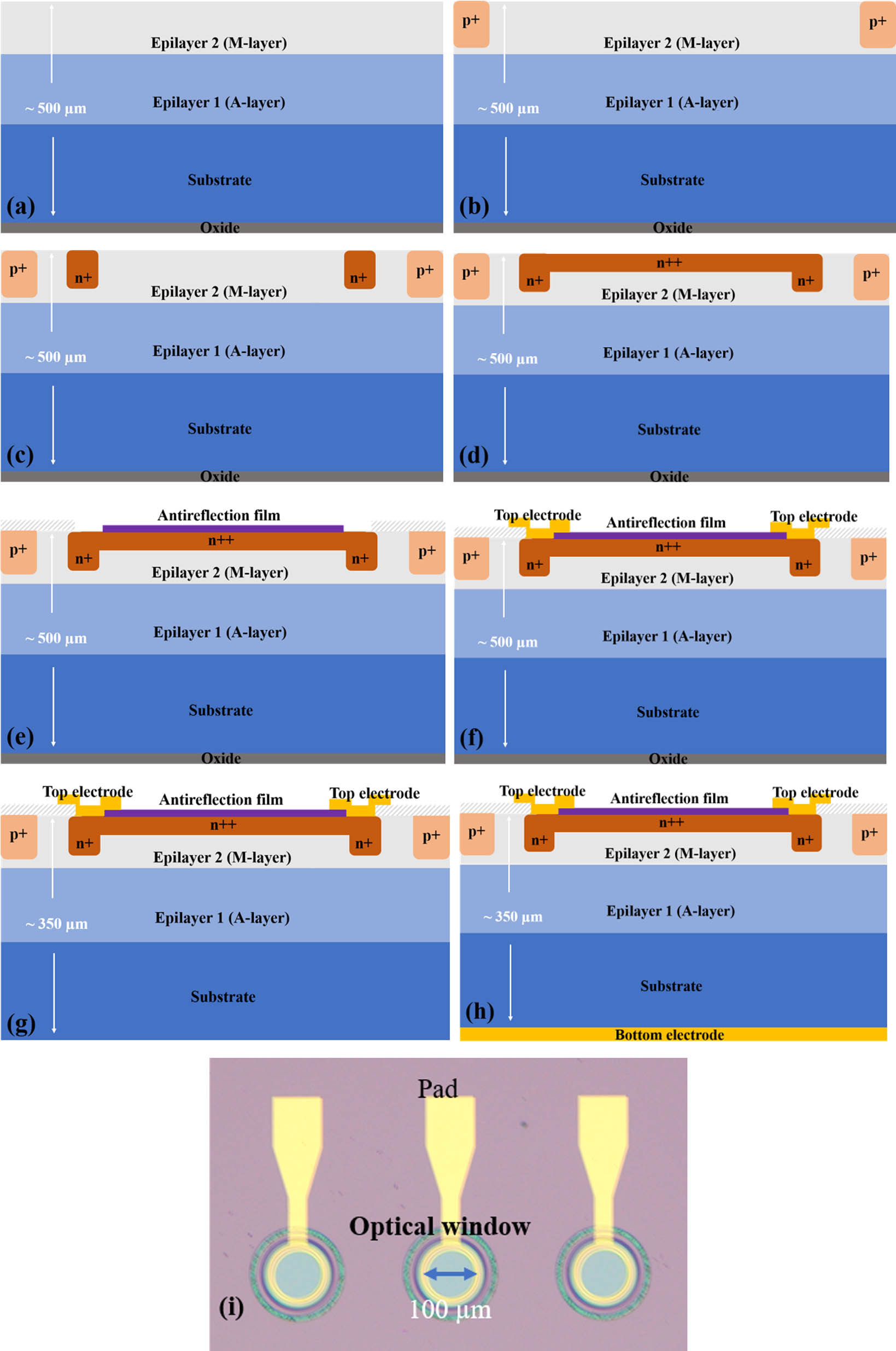
    Fig. 1. Key fabrication process of the silicon APD array and microscope photograph of partial fabricated arrays. (a) Epitaxial wafer growth; (b) implantation of P-stopper; (c) implantation of guard-ring and rapid thermal annealing; (d) implantation for ohm contact and rapid thermal annealing; (e) antireflection film deposited and etched; (f) TiAu deposition and patterning; (g) CMP on the back side; (h) metallization on the back side; (i) microscope photograph of partial fabricated arrays.
    Brief schematic of the APD arrays measurement system (a monochromatic light source was used in the actual measurement).
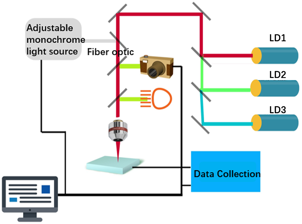
    Fig. 2. Brief schematic of the APD arrays measurement system (a monochromatic light source was used in the actual measurement).
    Uniformity of 2 × 64 fabricated APD arrays. (a) Dark currents of all pixels as a function of reverse bias voltage; (b) profile of breakdown voltage and dark current at unity gain; (c) two-dimensional mapping of dark current at unity gain (unit, pA); (d) two-dimensional mapping of Vbr for pixels.
    Fig. 3. Uniformity of 2 × 64 fabricated APD arrays. (a) Dark currents of all pixels as a function of reverse bias voltage; (b) profile of breakdown voltage and dark current at unity gain; (c) two-dimensional mapping of dark current at unity gain (unit, pA); (d) two-dimensional mapping of Vbr for pixels.
    Measurement results of response and multiplication characteristics for one pixel in the fabricated APD arrays. (a) Response characteristics at unity gain; (b) reverse I-V curves near breakdown state.
    Fig. 4. Measurement results of response and multiplication characteristics for one pixel in the fabricated APD arrays. (a) Response characteristics at unity gain; (b) reverse I-V curves near breakdown state.
    Dynamic characteristics for one pixel. (a) Capacitance versus reverse voltage; (b) quick optical pulse response of standard ET2020 APD; (c) quick optical pulse response of fabricated APD in this work.
    Fig. 5. Dynamic characteristics for one pixel. (a) Capacitance versus reverse voltage; (b) quick optical pulse response of standard ET2020 APD; (c) quick optical pulse response of fabricated APD in this work.
    EpilayerDoping concentration (cm3)Thickness (μm)
    Multiplication layer1×1015 (p-type)5
    Absorption layer5×1012 (p-type)35
    Table 1. Epistructure of the Device
     Ref.Apixel (mm2)NpixelVariationEQE (850 nm)VBR (V)
    1[17]81.924×815%78%400
    2[18]4.12×85%82%200
    3[19]1.952×85%80%150
    4This work12.62×643%81%105
    Table 2. Performance Comparison of Different Reported Silicon Avalanche Photodiode Arrays
    Tiancai Wang, Peng Cao, Hongling Peng, Chuanwang Xu, Haizhi Song, Wanhua Zheng. High-uniformity 2 × 64 silicon avalanche photodiode arrays with silicon multiple epitaxy technology[J]. Chinese Optics Letters, 2023, 21(3): 032501
    Download Citation