
Kanglin Li, Jiangbing Du, Weihong Shen, Jiacheng Liu, Zuyuan He. Improved optical coupling based on a concave cavity lens fabricated by optical fiber facet etching[J]. Chinese Optics Letters, 2021, 19(5): 050602
- Chinese Optics Letters
- Vol. 19, Issue 5, 050602 (2021)
Abstract
Keywords
1. Introduction
With the continuously increasing demand of Internet services and applications, the bandwidth of the optical fiber communication network increases by 30%–50% every year[
In order to improve the coupling efficiency between the fiber and the PIC, the fiber lens is widely used[
In this work, we propose a low-fabrication-complexity concave cavity lens fabricated by optical fiber facet etching, the so-called facet etched cavity lens (FECL). The FECL is designed for shrinking the optical field area output from the fiber so as to improve optical coupling between the fiber and PICs. The fabrication principle of FECL is based on the graded index of the fiber showing different etching rates. Here, we chose the graded-index nine-mode fiber (NMF) to fabricate the FECL. We demonstrated the single-mode coupling between the fiber and on-chip waveguide [TE0-linearly polarized (LP01)] for supporting standard applications and high-order mode coupling (TE1-LP11) for supporting mode division multiplexing (MDM) applications.
Sign up for Chinese Optics Letters TOC. Get the latest issue of Chinese Optics Letters delivered right to you!Sign up now
Numerical simulation results show that the effective spot area of the fundamental mode (LP01) output from the FECL can be reduced from 152.17 to , and the effective area of the LP11 mode can be reduced from 276.91 to . The coupling loss of the fundamental mode between the FECL and on-chip inverse taper is reduced to 2.9 dB, and the coupling loss of the LP11 mode to the integrated Y-junction waveguide is down to 0.55 dB. The longitudinal tolerance for 80% coupling efficiency exceeds 20 µm.
2. Principle and Design
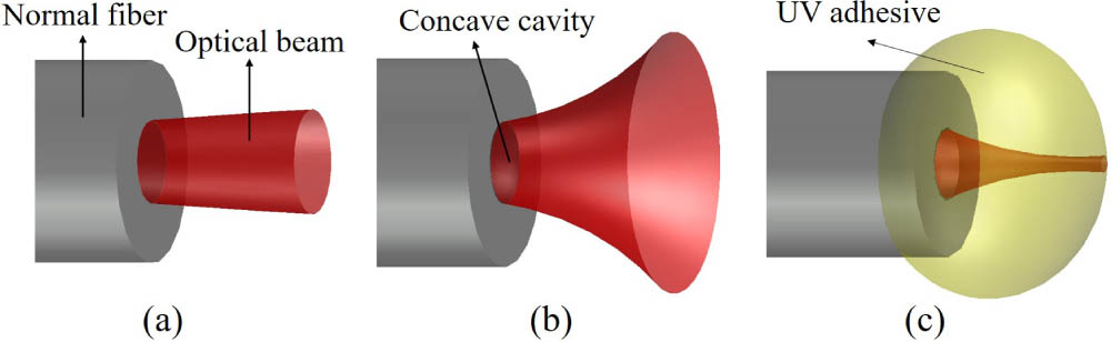
The FECL can be only formed on the fiber facet with the graded index decreasing from the center to around. Thus, we used an NMF to make the experimental demonstration, for instance. The fabrication process of the FECL is also applicable for other graded-index fibers, and the light focusing effect is the same. Figure 1 shows the schematic diagram of the proposed FECL for light focusing. The optical beam from the fiber before etching has a certain divergence angle, which is related to the numerical aperture (NA) of the fiber, as shown in Fig. 1(a). When coupling from the fiber to integrated waveguides, large coupling loss will be induced due to the large optical field mismatch as well as the divergence angle. After facet etching to form the concave cavity, the optical beam would be enlarged due to the increased divergence angle induced by the cavity, as shown in Fig. 1(b). However, after filling the concave cavity with high-index UV adhesive, the concave cavity becomes a convex lens, the so-called FECL, as shown in Fig. 1(c). Consequently, the optical beam is shrunk by the FECL. Simultaneous optical packaging can be realized after UV curing to solidify the adhesive. The focusing effect as well as the optical packaging performance of the FECL is highly dependent on the facet cavity structure and adhesive index.
![]()
Figure 1.Schematic diagram of the output optical beam from (a) a normal fiber facet, (b) the fiber facet with concave cavity, and (c) the FECL with UV adhesive.
Chemical etching is a very simple and low-cost method to fabricate the facet concave cavity. The principle of the fabrication is based on the different etching speeds between the core and the cladding. For standard fibers with germanium-doped cores and pure silica cladding, the core has a faster etching speed than the cladding in HF acid solution[
Figure 2 shows the fabrication process for the FECL with several steps: (a) fiber facet etching by simply putting the fiber end into the HF acid solution, with certain conditions of HF concentration, temperature, as well as etching duration; (b) fiber facet cleaning using alkaline water, alcohol, and clear water in turn; (c) drying up the fiber and forming the concave cavity on the fiber facet; (d) filling up the cavity and the gap between the fiber facet and photonic device with UV adhesive; (e) UV curing for solidifying the adhesive; (f) optical packaging completed.
![]()
Figure 2.Schematic of the FECL fabrication process.
Shown in Fig. 3 are the measured microscope images and height distribution diagram of two kinds of fibers after the HF acid etching: graded-index NMF and graded-index optical multimode (OM4) fiber. As expected, the core and the cladding have different etching speeds; thus, cavities can be realized after a period of etching time. As for the graded-index fibers in Figs. 3(a) and 3(c), the facet microcavities are in paraboloid-like shape, so as to support the formation of the FECL. The sectional height distribution diagrams of the NMF and OM4 fiber measured by optical three-dimensional (3D) microscope are shown in Figs. 3(b) and 3(d), showing a clear concave cavity on the fiber facet.
![]()
Figure 3.Measured microscope images and sectional height profiles of the etched fiber facet: (a) NMF facet, (b) NMF height profile, (c) OM4 multimode fiber facet, (d) OM4 multimode fiber height profile.
We investigated the optical coupling of the FECL based on the NMF for both the fundamental mode and high-order mode for MDM applications. The NMF, as one kind of few-mode fiber, has a graded-index core profile with 33 µm core diameter and 125 µm cladding diameter. The core of this fiber is doped by germanium with the highest refractive index at the core center, and the cladding is pure silicon dioxide. Thus, the refractive index reaches the peak at the core center, and gradually decreases from the center. Such distribution of the refractive index is necessary to form the FECL after HF etching.
We carried out the experiment of NMF facet etching with different etching time. Shown in Fig. 4 is the cavity depth curve as a function of etching time with 50% HF concentration acid under room temperature of 25°C. The linear fitting coefficient of the curve is , indicating that the cavity depth is proportional to the etching time, which is in good agreement with previous works[
![]()
Figure 4.(a) Measured cavity depths of NMF under etching time varying from 8 to 30 min. (b) and (c) are height profiles with paraboloid fitting after 12 min and 28 min etching, respectively.
We measured the profile of the facet cavity by using a high-resolution 3D microscope, as shown in Fig. 4. The height profiles of the cavities are shown in Figs. 4(b) and 4(c) after 12 min and 28 min etching, respectively. Paraboloid fitting, with a function of , is used for characterizing the cavities with fitting accuracy of 0.1 µm. represents the parabolic coefficient, which is related to the curvature of the facet cavity and determined by the etching time. The fitting coefficients of Figs. 4(b) and 4(c) are 0.9831 and 0.9617, respectively.
Another important factor determining the FECL performance is the refractive index of the UV adhesive (). Generally, when using UV adhesive with a higher refractive index, better focusing performance of the FECL can be realized. The UV adhesive with the highest refractive index available in the market is about 1.65. Thus, we use the adhesive refractive index around 1.6 for further investigations. We carried out simulations for the FECL to verify the optical focusing effect, for both fundamental mode and high-order mode. The simulation is adopted by the 3D finite-difference time-domain (FDTD) method.
3. FECL for Optical Focusing
Figure 5 shows the output optical fields of the fundamental mode from the NMF facet in three different cases, without etching, with facet etched concave cavity (), and FECL after high-index UV adhesive () filling, respectively. One can clearly observe the optical focusing effect after the FECL due to the formation of a convex lens on the fiber facet. Under different FECL structures (i.e., different shape coefficient and index of the facet lens), we can obtain different optical focusing performance for various optical coupling applications.
![]()
Figure 5.Simulated optical beam field of the output fundamental mode: (a) NMF without etching, (b) facet cavity without filling the UV adhesive, and (c) FECL with UV adhesive.
The output optical beams of the fundamental mode after different FECLs are shown in Figs. 6(a)–6(d), with ranging from 0.09 to 0.15 at a step of 0.02, while is fixed to 1.6, and the optical wavelength is fixed at 1550 nm. Steady enhancement of optical focusing can be observed clearly. Then, we fix at 0.12 and hold the optical wavelength at 1550 nm, and the output optical beams are shown in Figs. 6(e)–6(f) after FECL with ranging from 1.56 to 1.68 at a step of 0.04. Improved optical focusing can also be observed along with the increased adhesive index, which is in good agreement with our above-mentioned predictions.
![]()
Figure 6.Simulated fundamental mode optical beams: (a) K
Here, we define the effective area reduction ratio to estimate the performance of optical beam focusing, which is calculated by the ratio of the effective field area between the original fundamental mode and the waist after FECL. Figure 7 shows the to and . In the NMF, the original effective area of the fundamental mode is as large as , as shown in the inset figure of Fig. 7(1). Figures 7(2)–7(5) present the optical field of the fundamental mode after FECL at the focus plane, which has the minimum optical field. With typical value of 1.64 for the UV adhesive index and 0.14 for , a shrunken area of only is obtained.
![]()
Figure 7.Simulated reduction of the effective area of fundamental mode. The inset figures: (1) fundamental mode in the NMF; (2)–(5) shrunken mode fields of different FECLs.
The focusing performance of FECL is also affected by the longitudinal offset, as shown in Fig. 8, in which the spot effective area varies along with different longitudinal displacements. The reference position is 12 µm from the FECL, with changing from 0.09 to 0.14 and fixed at 1.6, so as to reach the beam waist.
![]()
Figure 8.Simulated longitudinal displacement tolerance of fundamental mode spot effective area at different K.
The focusing performance of higher-order mode LP11 after FECL is also investigated, as shown in Fig. 9. The propagated optical beams are shown in Figs. 9(a)–9(d), with changing from 0.09 to 0.15 at a step of 0.02, and fixed at 1.6 at a wavelength of 1550 nm. The value is fixed at 0.12, and the is changed from 1.56 to 1.68 at a step of 0.04, as shown in Fig. 9(e)–9(h).
![]()
Figure 9.Simulated LP11 mode optical field simulation: (a) K
We calculated the LP11 mode effective area at the waist after different FECLs. Shown in Fig. 10 is the effective area reduction ratio as a function of and . The original optical effective area of the LP11 mode is as large as , as shown in Fig. 10(1). The optical field of the LP11 mode after the FECL at the focus plane of the FECL has the minimum optical field, as shown in the inset figures of Fig. 10(2)–10(5). A shrunken area of can be obtained, with value of 1.64 for the UV adhesive index and 0.14 for . The tolerance of the longitudinal offset of the spot effective area is shown in Fig. 11, with changing from 0.09 to 0.14, and fixed at 1.6.
![]()
Figure 10.Simulated reduction of the effective area of the LP11 mode. The inset figures: (1) LP11 mode in the NMF; (2)–(5) shrunken mode fields after different FECLs.
![]()
Figure 11.Simulated longitudinal displacement tolerance of the LP11 mode spot effective area after different FECLs. Displacement from the minimum spot area from plus to minus 12 µm.
In this work, we mainly investigate the performance of FECL by simulating the coupling loss of FECL to photonic chips. An inverse taper can be used for on-chip transmission of the fundamental mode; but, for high-order modes, we need specially shaped waveguides like the Y-junction inverse taper. The schematic diagrams of these waveguides are shown in Fig. 12. The dimension of the inverse taper is fixed, as shown in Fig. 12(a). The widths of the waveguide tip and main waveguide are 150 nm and 450 nm, respectively. The height of the waveguide , is 220 nm as shown in Fig. 12(b). Figure 12(c) is the schematic diagram of the Y-junction inverse taper waveguide, in which two separated inverse tapers are combined into one main waveguide. Three structural parameters including the width of the taper tip (), the width of the main waveguide (), and the distance between the two inverse tapers () can be optimized.
![]()
Figure 12.Schematic diagram of two kinds of inverse tapers: (a), (b) the top view and sectional view of the inverse taper and (c) top view of the Y-junction inverse taper waveguide.
The coupling efficiencies of edge coupling from the FECL to inverse tapers are calculated for characterizing the coupling functionality of the FECL. Figure 13 shows the fundamental mode longitudinal and lateral coupling loss tolerance from the FECL to the inverse taper, under different values and a fixed value of at 1.6. Generally, the better the matching between the focused mode field of the FECL and the inverse taper, the higher the coupling efficiency realized. It can be found that higher value leads to higher optimal coupling efficiency, but with lower coupling tolerance, as shown in Fig. 13.
![]()
Figure 13.Simulated coupling efficiency of the fundamental mode from the FECL to the inverse taper under different cavity coefficient K: (a) longitudinal coupling tolerance along with longitudinal displacement and (b) lateral coupling tolerance along with horizontal alignment.
Table 1 shows the optimal coupling distance and 80% coupling tolerance of fundamental mode coupling from the NMF FECL to the inverse taper. The coupling distance (about 20 µm) and tolerance in the longitudinal direction (mainly over 30 µm) of the proposed FECL are both larger than those of the conventional fiber lens. Besides, the use of FECL can also simplify the packaging, leading to reduced packaging cost and higher yield.
| 0.09 | 0.10 | 0.11 | 0.12 | 0.13 | 0.14 | |
|---|---|---|---|---|---|---|
| Optimal coupling distance (µm) | 34 | 28 | 23 | 17 | 13 | 9 |
| 80% longitudinal tolerance (µm) | 29 | 20 | ||||
| 80% lateral tolerance (µm) | 2.0 | 1.8 | 1.6 | 1.6 | 1.5 | 1.4 |
Table 1. Simulated Optimal Coupling Distance, Longitudinal and Lateral 80% Coupling Tolerance of Fundamental Mode Coupling from Fiber to Inverse Taper
The high-order mode (LP11) edge coupling needs a special shape of waveguide like the Y-junction inverse taper waveguide, as shown in Fig. 12(c). The two separated inverse tapers can be well coupled with the two speckles of the LP11 mode. Besides and , the distance between the two inverse tapers () also deeply affects the coupling efficiency. With the improvement of the optical focusing effect, the value of needs to be reduced for more accurate coupling. Figure 14 shows the longitudinal and lateral tolerance for LP11 coupling from the fiber to the Y-junction waveguide. The coupling loss firstly increases along with the lateral displacement, and then a small reduction is observed, which is due to the leaking of the optical field when the lateral displacement is too large, as shown in Fig. 14(b). The 80% coupling loss and optimal are shown in Table 2, and the optimal coupling distance of the LP11 mode is almost the same as the fundamental mode.
| 0.09 | 0.10 | 0.11 | 0.12 | 0.13 | 0.14 | |
|---|---|---|---|---|---|---|
| 4.1 | 4.0 | 3.7 | 3.6 | 3.4 | 3.4 | |
| 80% longitudinal tolerance (µm) | 29 | 20 | ||||
| 80% lateral tolerance (µm) | 2.0 | 1.8 | 1.6 | 1.6 | 1.5 | 1.4 |
Table 2. Simulated Optimal
![]()
Figure 14.Simulated coupling efficiency of the LP11 mode coupling from the fiber to the Y-junction inverse taper with different K: (a) coupling tolerance at the optimal coupling point in the longitudinal direction and (b) lateral coupling tolerance of the coupling efficiency.
The wideband transmission of the fundamental mode and high-order mode coupling is also investigated as shown in Fig. 15. For the fundamental mode in Fig. 15(a), the 3 dB bandwidth is over 1000 nm. For the high-order mode LP11 in Fig. 15(b), the 3 dB bandwidth is smaller, but still over 900 nm.
![]()
Figure 15.Simulated transmission spectrum of the FECL coupling to inverse taper for (a) the fundamental mode and (b) the LP11 mode.
The reason why we have not carried out the coupling experiment was limited by objective factors; according to our simulation, in order to achieve high coupling efficiency from the FECL to the optical waveguide, the parabolic coefficient K, which is related to the curvature of the facet cavity, must reach about 0.13, where the corresponding corrosion depth is about 35 µm. However, although we found the linear relationship between etching depth and time, limited by our experimental conditions, the shape and depth of the microcavity formed by HF acid corrosion for a long time are not ideal. But, the desired experimental results have been realized in other’s work[
4. Conclusion
As a conclusion, in this work, we propose a new kind of fiber lens named FECL for optical coupling with low-fabrication-complexity and wideband operation. The FECL is fabricated by fiber facet etching and filling the high refractive index UV adhesive in the etched concave cavity. The simulation results show that, at the wavelength of 1550 nm, the fundamental mode spot area of the NMF can be reduced from 152.17 to , and the effective area of the LP11 mode can be reduced from 276.91 to . The edge coupling loss from the NMF to the integrated waveguide is 2.9 dB with over 1000 nm 3 dB bandwidth, and the coupling loss of the LP11 mode to the Y-junction waveguide is reduced to 0.55 dB with over 900 nm 3 dB bandwidth. In addition to optical coupling between fibers and photonic waveguides, the proposed FECL also has great potential for other optical coupling and packaging applications.
References
[4] L. Ma, S. Jiang, J. Du, C. Yang, W. Tong, Z. He. Ring-assisted 7-lp-mode fiber with ultralow inter mode crosstalk. Asia Communications and Photonics Conference 2016, AS4A.5(2016).
[7] J. Li, J. Du, L. Ma, M.-J. Li, Z. He. Second-order few mode distributed Raman amplifier for mode-division multiplexing transmission. Optical Fiber Communication Conference, Th4A.3(2017).
[8] G. Son, S. Han, J. Park, K. Kwon, K. Yu. High-efficiency broadband light coupling between optical fibers and photonic integrated circuits. Nanophotonics, 10, 1515(2018).
[22] F. P. Payne, C. D. Hussey, M. S. Hataki. Modelling fused single-mode fibre couplers. Electron. Lett., 21, 461(1985).
[23] S.-M. Tseng, C.-L. Chen. Side-polished fibers. Appl. Opt., 31, 3438(1992).
[28] P. A. R. Tafulo, P. A. S. Jorge, J. L. Santos, O. Frazão. Fabry–Pérot cavities based on chemical etching for high temperature and strain sensing. Opt. Commun., 285, 1159(2012).
[29] C. J. Tuck, R. Hague, C. Doyle. Low cost optical fibre based Fabry–Perot strain sensor production. Meas. Sci. Technol., 17, 2206(2006).

Set citation alerts for the article
Please enter your email address
© Copyright 2018-2021 | Chinese Laser Press. All Rights Reserved 沪ICP备15018463号-20