• Advanced Photonics
  • Vol. 5, Issue 3, 034002 (2023)
Qiang Luo, Fang Bo*, Yongfa Kong, Guoquan Zhang, and Jingjun Xu
Author Affiliations
  • Nankai University, TEDA Institute of Applied Physics and School of Physics, MOE Key Laboratory of Weak-Light Nonlinear Photonics, Tianjin, China
  • show less
    DOI: 10.1117/1.AP.5.3.034002 Cite this Article Set citation alerts
    Qiang Luo, Fang Bo, Yongfa Kong, Guoquan Zhang, Jingjun Xu. Advances in lithium niobate thin-film lasers and amplifiers: a review[J]. Advanced Photonics, 2023, 5(3): 034002 Copy Citation Text show less
    Research field overview of LNOI light sources and amplifiers, which can be roughly classified into three parts: the optical-pump REI-doped devices and electrical-pump III/V devices and their applications. Some schematic sources: M-M (multi-mode) laser, reprinted from Ref. 27; S-M (single-mode) laser, reprinted from Ref. 28; amplifier, reprinted from Ref. 29; Hybrid laser, reprinted from Ref. 30, © 2021 Optica; hetero laser, reprinted from Ref. 31, © 2021 Optica; printing laser, reprinted from Ref. 32, © 2021 Optica; transmitter, reprinted from Ref. 33, © 2021 Optica; tunable laser, reprinted from Ref. 34 under a CC-BY license.
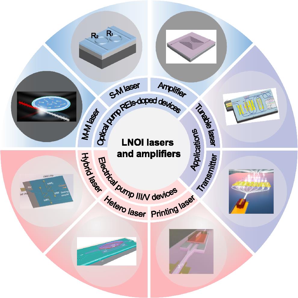
    Fig. 1. Research field overview of LNOI light sources and amplifiers, which can be roughly classified into three parts: the optical-pump REI-doped devices and electrical-pump III/V devices and their applications. Some schematic sources: M-M (multi-mode) laser, reprinted from Ref. 27; S-M (single-mode) laser, reprinted from Ref. 28; amplifier, reprinted from Ref. 29; Hybrid laser, reprinted from Ref. 30, © 2021 Optica; hetero laser, reprinted from Ref. 31, © 2021 Optica; printing laser, reprinted from Ref. 32, © 2021 Optica; transmitter, reprinted from Ref. 33, © 2021 Optica; tunable laser, reprinted from Ref. 34 under a CC-BY license.
    Methods for REI doping into LN crystal and the corresponding concentration-depth distribution. (a) and (d) Crystal growth doping; (b) and (e) thermal diffusing doping; and (c) and (f) ion implantation doping. C, doping concentration and Cmax, the available maximum doping concentration for the corresponding method.
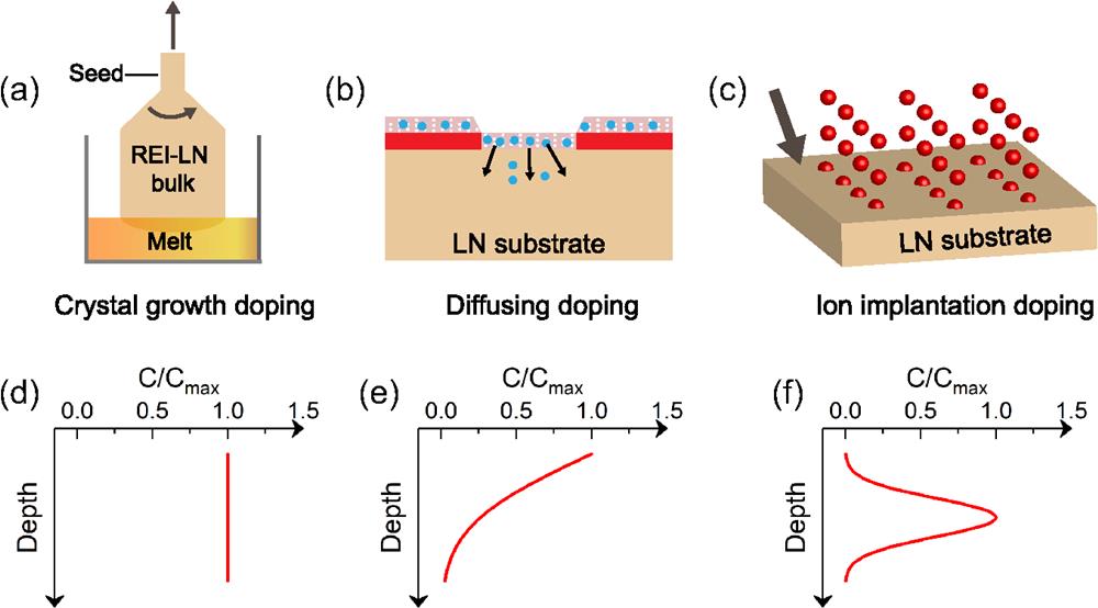
    Fig. 2. Methods for REI doping into LN crystal and the corresponding concentration-depth distribution. (a) and (d) Crystal growth doping; (b) and (e) thermal diffusing doping; and (c) and (f) ion implantation doping. C, doping concentration and Cmax, the available maximum doping concentration for the corresponding method.
    (a) Schematic of the thulium-doped LNOI waveguide with grating couplers. Reprinted with permission from Ref. 47, © 2020 American Chemical Society. (b) SEM image and concentration distribution of erbium ions implanted in LNOI structure. Reprinted from Ref. 48, with the permission of AIP Publishing. (c) Schematic cross-sectional diagram and SRIM simulation distribution of ytterbium ions implanted in LNOI structure. Reprinted from Ref. 49, with the permission of AIP Publishing. (d) Schematic diagram of ytterbium ions implanted in LNOI tunable microcavities. Reprinted from Ref. 50, © 2022 Optica. (e) Optical micrograph of the LNOI device and schematic cross-sectional drawing after bonding with Er3+:Y2SiO5. Reprinted from Ref. 51, © 2021 Optica. (f) Schematic cross-sectional view of the Er:LN crystal integrated with Si-SiN waveguides and resonators. Reprinted from Ref. 52, with the permission of AIP Publishing.
    Fig. 3. (a) Schematic of the thulium-doped LNOI waveguide with grating couplers. Reprinted with permission from Ref. 47, © 2020 American Chemical Society. (b) SEM image and concentration distribution of erbium ions implanted in LNOI structure. Reprinted from Ref. 48, with the permission of AIP Publishing. (c) Schematic cross-sectional diagram and SRIM simulation distribution of ytterbium ions implanted in LNOI structure. Reprinted from Ref. 49, with the permission of AIP Publishing. (d) Schematic diagram of ytterbium ions implanted in LNOI tunable microcavities. Reprinted from Ref. 50, © 2022 Optica. (e) Optical micrograph of the LNOI device and schematic cross-sectional drawing after bonding with Er3+:Y2SiO5. Reprinted from Ref. 51, © 2021 Optica. (f) Schematic cross-sectional view of the Er:LN crystal integrated with Si-SiN waveguides and resonators. Reprinted from Ref. 52, with the permission of AIP Publishing.
    (a) The emitted laser signal at the 1560-nm band under the 976 nm laser pump. Inset: the accompanied green-up conversion fluorescence. Reprinted from Ref. 70, © 2021 Optica. (b) The observed signal wavelength drift process with different pump powers for the 974 nm pump. Reprinted from Ref. 27. (c) The dependence of the dominant mode signal power on the pump power. Reprinted from Ref. 71. (d) The collected spectra at different pump power. (e) The observed SHG and SFG at the 969 nm laser pump. Inset, the captured photograph of the microdisk at the visible (left) and IR (right) regions. (d) and (e) Reprinted from Ref. 72, © 2021 Optica. (f) The dependence of signal power (squares) and linewidth (circles) of the dominating lasing mode on the increasing pump power. Reprinted from Ref. 73, © 2022 Optica.
    Fig. 4. (a) The emitted laser signal at the 1560-nm band under the 976 nm laser pump. Inset: the accompanied green-up conversion fluorescence. Reprinted from Ref. 70, © 2021 Optica. (b) The observed signal wavelength drift process with different pump powers for the 974 nm pump. Reprinted from Ref. 27. (c) The dependence of the dominant mode signal power on the pump power. Reprinted from Ref. 71. (d) The collected spectra at different pump power. (e) The observed SHG and SFG at the 969 nm laser pump. Inset, the captured photograph of the microdisk at the visible (left) and IR (right) regions. (d) and (e) Reprinted from Ref. 72, © 2021 Optica. (f) The dependence of signal power (squares) and linewidth (circles) of the dominating lasing mode on the increasing pump power. Reprinted from Ref. 73, © 2022 Optica.
    (a) Collected power of signal mode under different pump powers. Inset: the captured green up-conversion fluorescence. Reprinted from Ref. 77, © 2021 Optica. (b) The detected emission spectra at different pump power. Inset: schematic of the bonding process for the microring and waveguide structures. (c) The recorded signal spectrum at 1533 nm for the varying electric voltage between −300 and +300 V. (b) and (c) Reprinted from Ref. 78, © 2021 Optica. (d) Observed multi-peak signals at a pump power of ∼2.23 mW. (e) The signal power (blue square) and linewidth (red circle) of the dominant mode as a function of pump power. (d) and (e) Reprinted from Ref. 79, © 2022 Optica.
    Fig. 5. (a) Collected power of signal mode under different pump powers. Inset: the captured green up-conversion fluorescence. Reprinted from Ref. 77, © 2021 Optica. (b) The detected emission spectra at different pump power. Inset: schematic of the bonding process for the microring and waveguide structures. (c) The recorded signal spectrum at 1533 nm for the varying electric voltage between 300 and +300  V. (b) and (c) Reprinted from Ref. 78, © 2021 Optica. (d) Observed multi-peak signals at a pump power of 2.23  mW. (e) The signal power (blue square) and linewidth (red circle) of the dominant mode as a function of pump power. (d) and (e) Reprinted from Ref. 79, © 2022 Optica.
    (a) Single-mode lasing spectra at different pump power. Inset: SEM image of the fabricated coupled microdisks. Reprinted from Ref. 80, © 2021 Optica. (b) Single-mode lasing signal with a high SMSR in coupled microrings at a pump power of about 900 μW. Inset: the observed green up-conversion fluorescence in the photonic molecule. Reprinted from Ref. 28. (c) Single-mode laser power under different pump power. Inset: schematic diagram of the coupled microdisk and microring. Reprinted from Ref. 81, © 2021 Optica. (d) Schematic diagram of dual cavity laser and the operation principle of single-frequency laser. (e) Single frequency laser emission spectrum with an SMSR of 31 dB. Inset: the photograph of the designed dual cavity. (d) and (e) Reprinted from Ref. 82, © 2021 Optica.
    Fig. 6. (a) Single-mode lasing spectra at different pump power. Inset: SEM image of the fabricated coupled microdisks. Reprinted from Ref. 80, © 2021 Optica. (b) Single-mode lasing signal with a high SMSR in coupled microrings at a pump power of about 900  μW. Inset: the observed green up-conversion fluorescence in the photonic molecule. Reprinted from Ref. 28. (c) Single-mode laser power under different pump power. Inset: schematic diagram of the coupled microdisk and microring. Reprinted from Ref. 81, © 2021 Optica. (d) Schematic diagram of dual cavity laser and the operation principle of single-frequency laser. (e) Single frequency laser emission spectrum with an SMSR of 31 dB. Inset: the photograph of the designed dual cavity. (d) and (e) Reprinted from Ref. 82, © 2021 Optica.
    (a) Simulated mode profile for the four supported modes. (b) Collected single-mode laser emission spectra. Inset: the pump spectra after passing through the microring. (a) and (b) Reprinted from Ref. 83 under a CC-BY license. (c) Observed single-mode laser with a 37 dB SMSR. Inset: a captured image of the excited polygon modes for lasing signal, upconversion fluorescence, and pump, respectively. (d) Single-mode lasing wavelength at different applied voltages. (c) and (d) Reprinted from Ref. 84 under a CC-BY license. (e) Recorded signal spectra in the range of 1500–1600 nm with increasing pump power. Inset: the observed green upconversion fluorescence of the pumped microring. Reprinted from Ref. 85, © 2022 Optica. (f) Observed single-frequency lasing spectrum at 1544.658 nm with a pump power of 18 mW. Inset: the electrode configuration schematic of the tunable microdisk laser. Reprinted from Ref. 86.
    Fig. 7. (a) Simulated mode profile for the four supported modes. (b) Collected single-mode laser emission spectra. Inset: the pump spectra after passing through the microring. (a) and (b) Reprinted from Ref. 83 under a CC-BY license. (c) Observed single-mode laser with a 37 dB SMSR. Inset: a captured image of the excited polygon modes for lasing signal, upconversion fluorescence, and pump, respectively. (d) Single-mode lasing wavelength at different applied voltages. (c) and (d) Reprinted from Ref. 84 under a CC-BY license. (e) Recorded signal spectra in the range of 1500–1600 nm with increasing pump power. Inset: the observed green upconversion fluorescence of the pumped microring. Reprinted from Ref. 85, © 2022 Optica. (f) Observed single-frequency lasing spectrum at 1544.658 nm with a pump power of 18 mW. Inset: the electrode configuration schematic of the tunable microdisk laser. Reprinted from Ref. 86.
    (a) The obtained internal net gain at 1530 nm with increasing pump. Inset: observed green upconversion fluorescence under the 980 nm laser pump. (b) The measured signal gain at different wavelengths. Inset: spontaneous spectrum measured in erbium-doped LN waveguide. Inset: detected spontaneous spectrum measured in erbium-doped LN waveguide. (a) and (b) Reprinted from Ref. 111. (c) Measured signal spectra as a function of increasing pump powers measured at 1531.6 nm. Reprinted from Ref. 112, © 2021 Optica. (d) Dependence of internal net gain at 1531.5 nm on the signal power. Inset: observed green upconversion fluorescence in the compact waveguide. Reprinted from Ref. 113. (e) The measured net gain for Ta2O5-clad waveguide amplifiers and Air-clad waveguide amplifiers. Inset: the cross-sectional schematic of the erbium-doped LNOI waveguide amplifiers with Ta2O5-cladding. Reprinted from Ref. 114 under a CC-BY license. (f) The measured net gain of ytterbium-doped LNOI waveguide amplifiers at the different pump powers and the signal wavelength of 1060 nm. Inset: the photography of the ytterbium-doped LNOI waveguide. Reprinted from Ref. 115 under a CC-BY license.
    Fig. 8. (a) The obtained internal net gain at 1530 nm with increasing pump. Inset: observed green upconversion fluorescence under the 980 nm laser pump. (b) The measured signal gain at different wavelengths. Inset: spontaneous spectrum measured in erbium-doped LN waveguide. Inset: detected spontaneous spectrum measured in erbium-doped LN waveguide. (a) and (b) Reprinted from Ref. 111. (c) Measured signal spectra as a function of increasing pump powers measured at 1531.6 nm. Reprinted from Ref. 112, © 2021 Optica. (d) Dependence of internal net gain at 1531.5 nm on the signal power. Inset: observed green upconversion fluorescence in the compact waveguide. Reprinted from Ref. 113. (e) The measured net gain for Ta2O5-clad waveguide amplifiers and Air-clad waveguide amplifiers. Inset: the cross-sectional schematic of the erbium-doped LNOI waveguide amplifiers with Ta2O5-cladding. Reprinted from Ref. 114 under a CC-BY license. (f) The measured net gain of ytterbium-doped LNOI waveguide amplifiers at the different pump powers and the signal wavelength of 1060 nm. Inset: the photography of the ytterbium-doped LNOI waveguide. Reprinted from Ref. 115 under a CC-BY license.
    (a) The measured signal enhancement and internal net gain at different signal input power at 1531.6 nm. (b) The noise figure power and (c) the pump power conversion efficiency for different signal input power at 1531.6 nm. (d) The comparison of signal enhancement between 980 nm and 1484 nm pumps. Inset: modes distribution at 980 nm, 1484 nm, and 1530 nm. (e) The comparison of signal enhancement for different waveguide lengths. Inset: the simulation internal net gain at 1531.6 nm as a function of waveguide lengths. (f) The signal enhancement for different pumping schemes at 1531.6 nm. (a)–(f) Reprinted with permission from Ref. 117, © 2022 IEEE.
    Fig. 9. (a) The measured signal enhancement and internal net gain at different signal input power at 1531.6 nm. (b) The noise figure power and (c) the pump power conversion efficiency for different signal input power at 1531.6 nm. (d) The comparison of signal enhancement between 980 nm and 1484 nm pumps. Inset: modes distribution at 980 nm, 1484 nm, and 1530 nm. (e) The comparison of signal enhancement for different waveguide lengths. Inset: the simulation internal net gain at 1531.6 nm as a function of waveguide lengths. (f) The signal enhancement for different pumping schemes at 1531.6 nm. (a)–(f) Reprinted with permission from Ref. 117, © 2022 IEEE.
    The integrated schemes for electrically-pumped integrated photonics gain devices. (a) Schematic diagram of a typical inter-chip hybrid integrated laser. Reprinted from Ref. 135, © 2017 Optica. (b) Schematic diagram of a flip-chip hybrid integrated laser. Reprinted from Ref. 136, © 2017 Optica. (c) Left, illustration of heterogenous integration for wafer bonding. Reprinted from Ref. 134 under a CC-BY license. Right, schematic diagram of a heterogenous integration narrow-linewidth III-V/Si/Si3N4 laser realized by the wafer bonding techniques. Reprinted from Ref. 137, © 2022 Optica. (d) Left, illustration of micro-transfer printing technology. Reprinted from Ref. 129 under a CC-BY license. Right, schematic diagram of a heterogenous III-V-on-silicon-nitride mode-locked comb laser realized by the micro-transfer printing techniques. Reprinted from Ref. 138 under a CC-BY-NC-ND license.
    Fig. 10. The integrated schemes for electrically-pumped integrated photonics gain devices. (a) Schematic diagram of a typical inter-chip hybrid integrated laser. Reprinted from Ref. 135, © 2017 Optica. (b) Schematic diagram of a flip-chip hybrid integrated laser. Reprinted from Ref. 136, © 2017 Optica. (c) Left, illustration of heterogenous integration for wafer bonding. Reprinted from Ref. 134 under a CC-BY license. Right, schematic diagram of a heterogenous integration narrow-linewidth III-V/Si/Si3N4 laser realized by the wafer bonding techniques. Reprinted from Ref. 137, © 2022 Optica. (d) Left, illustration of micro-transfer printing technology. Reprinted from Ref. 129 under a CC-BY license. Right, schematic diagram of a heterogenous III-V-on-silicon-nitride mode-locked comb laser realized by the micro-transfer printing techniques. Reprinted from Ref. 138 under a CC-BY-NC-ND license.
    (a) Schematic of the tunable hybrid LNOI/III-V laser composed of an InP-based optical gain chip and an LNOI passive chip. (b) Recorded spectra of coarse wavelength tuning process. (a) and (b) Reprinted from Ref. 30, © 2021 Optica. (c) Schematic of the butt coupling of the electrically pumped hybrid laser. (d) Optical power inside the LNOI waveguide laser and voltage versus the laser driving current. Inset, the recorded lasing spectrum with the single-mode operation. (c) and (d) Reprinted from Ref. 33, © 2021 Optica. (e) Schematic illustration of lithium niobate integrated on Damascene platform (top) and self-injection locking principle (bottom) with laser wavelength tuning achieved by applying a voltage signal. Reprinted from Ref. 140 under a CC-BY license. (f) Single-sided power spectral density of frequency noise of the hybrid LNOI laser upon self-injection locking to racetrack resonator (red) and in free-running regime (green). Reprinted from Ref. 141. (g) The structure schematic of the hybrid integrated III-V/LNOI external cavity laser. (h) Laser frequency modulation rate as a function of modulation speed. (i) Observed dual-wavelength lasing spectra. (g)–(i) Reprinted from Ref. 34 under a CC-BY license.
    Fig. 11. (a) Schematic of the tunable hybrid LNOI/III-V laser composed of an InP-based optical gain chip and an LNOI passive chip. (b) Recorded spectra of coarse wavelength tuning process. (a) and (b) Reprinted from Ref. 30, © 2021 Optica. (c) Schematic of the butt coupling of the electrically pumped hybrid laser. (d) Optical power inside the LNOI waveguide laser and voltage versus the laser driving current. Inset, the recorded lasing spectrum with the single-mode operation. (c) and (d) Reprinted from Ref. 33, © 2021 Optica. (e) Schematic illustration of lithium niobate integrated on Damascene platform (top) and self-injection locking principle (bottom) with laser wavelength tuning achieved by applying a voltage signal. Reprinted from Ref. 140 under a CC-BY license. (f) Single-sided power spectral density of frequency noise of the hybrid LNOI laser upon self-injection locking to racetrack resonator (red) and in free-running regime (green). Reprinted from Ref. 141. (g) The structure schematic of the hybrid integrated III-V/LNOI external cavity laser. (h) Laser frequency modulation rate as a function of modulation speed. (i) Observed dual-wavelength lasing spectra. (g)–(i) Reprinted from Ref. 34 under a CC-BY license.
    (a) Top: schematic drawing of the different cross-sections for the heterogeneous integration platform. Bottom: schematic diagram of the designed ring laser and single-mode tunable laser. (b) Measured gain bandwidth of the III/V-on-LN amplifier. (c) Obtained LI curves of the ring laser at different temperatures. (d) Recorded spectra of the fine wavelength tuning of the single-mode laser. (a)–(d) Reprinted from Ref. 32, © 2021 Optica. (e) Optical microscopy image and SEM image of the cross-section of the heterogeneously integrated III-V-on-LN device. (f) Detected electroluminescence spectrum of the heterogeneously integrated III-V-on-LN broadband light sources. (e) and (f) Reprinted from Ref. 144, © 2022 Optica.
    Fig. 12. (a) Top: schematic drawing of the different cross-sections for the heterogeneous integration platform. Bottom: schematic diagram of the designed ring laser and single-mode tunable laser. (b) Measured gain bandwidth of the III/V-on-LN amplifier. (c) Obtained LI curves of the ring laser at different temperatures. (d) Recorded spectra of the fine wavelength tuning of the single-mode laser. (a)–(d) Reprinted from Ref. 32, © 2021 Optica. (e) Optical microscopy image and SEM image of the cross-section of the heterogeneously integrated III-V-on-LN device. (f) Detected electroluminescence spectrum of the heterogeneously integrated III-V-on-LN broadband light sources. (e) and (f) Reprinted from Ref. 144, © 2022 Optica.
    Schematic diagram of integrated optical chips based on LN thin film. SOA, semiconductor optical amplifier; RDFA, rare-earth-doped waveguide amplifier; PD, photodetector; and SHG, second-harmonic generation.
    Fig. 13. Schematic diagram of integrated optical chips based on LN thin film. SOA, semiconductor optical amplifier; RDFA, rare-earth-doped waveguide amplifier; PD, photodetector; and SHG, second-harmonic generation.
    DevicesPumpSignalReferences
    Wavelength (nm)Threshold (μW)Wavelength (nm)Power (nW)LinewidthConversion efficiencyModes or SMSR (dB)
    Disk9742.99×1031531.6400.12 nm4.12×106Multiple27
    14609.31×1031531.65000.14 nm3.15×105Multiple
    Disk976<4001563.31400.024 nm1.92×104Multiple70
    Disk9742921531.80.40.01  nm6.5×107Multiple71
    Disk98410310602.5×1035.3×103Multiple72
    Disk97621.1910603.7×1020.01  nm1.36×102Multiple73
    Ring974201532.40.10.01  nm6.61×107Multiple77
    Ring∼9803.5×1031530354.38×105Multiple78
    Ring97459.3210606.44×1030.01  nm5.45×104Multiple79
    Coupled disk977.72001550.550348 kHz7.0×105Single80
    Coupled ring979.62001531.1400.005  nm26.328
    Coupled ring148413.54×10315313.1×1021.2 MHz1.45×1043182
    Ring148414.51531.32.1×1031.27 MHz1.2×10435.583
    Disk9682515462×103322 Hz1.0×1043784
    Coupled disk and ring9741.31×1031560.4954.41×10531.481
    Ring97624.5×1031530.91×1020.045 nm8.33×10618.885
    Disk9761544.71029.1286
    Disk980485.51551.6862.1×1030.11 MHz4.78×10387
    Sagnac reflector9806×103154444.7×10328 pm1.8×1032588
    Table 1. Typical parameters comparison of reported REI-doped LNOI lasersa.
    WaveguidePumpSignalRef.
    Length (cm)Doping concentration (%)Wavelength (nm)Power (mW)Pumping schemesbWavelength (nm)Power (dBm)Internal net gain (dB)Gain per unit length (dB/cm)Output power (dBm)
    3.6198040Bi1530−47.185−29.07111
    26Bi1550−38.387.52.08−30.88
    0.50.598021For1531.6−50.865.210.4−45.66112
    21For1550−52.371.83.6−50.57
    0.50.1974∼23For1531.5−651530−50113
    0.53198010.78Bi1530−10.78.315.66−2.429
    2.8198045For1531.68.453.02119
    2.581148417.31Bi1531.6−50166.20−34117
    148418.54Bi1550−502.661.03−47.34
    10197663Bi1532−22202−2114
    40.597616For103051.25115
    97648For106082
    297614For15308498
    155052.5
    Table 2. Typical parameters comparison of reported REI-doped LNOI amplifiersa.
    Integrated methodsWorking wavelength (nm)Threshold current (mA)Output power (mW)Tuning range (nm)SMSR (dB)LinewidthReferences
    Hybrid integration1331.881002.536.46030
    Hybrid integration1558∼6060∼601 MHz33
    Hybrid integration1581.12805.5205011.3 kHz34
    Microtransfer printing∼1534∼850.7721∼40<1.5 MHz32
    Hybrid integration1555.45×103503.14 kHz140
    Hybrid integration1556.31>60141
    Heterogeneous integration16003.2×107144
    Hybrid integration1531.75005.8×1040.05 nm96
    Hybrid integration1328.3∼240.3>60475 kHz142
    Heterogeneous integration1590801.33031
    Table 3. Typical parameters comparison of reported electrically pumped LNOI lasers.a
    Qiang Luo, Fang Bo, Yongfa Kong, Guoquan Zhang, Jingjun Xu. Advances in lithium niobate thin-film lasers and amplifiers: a review[J]. Advanced Photonics, 2023, 5(3): 034002
    Download Citation