Lithium niobate (LN) thin film has received much attention as an integrated photonic platform, due to its rich and great photoelectric characteristics, based on which various functional photonic devices, such as electro-optic modulators and nonlinear wavelength converters, have been demonstrated with impressive performance. As an important part of the integrated photonic system, the long-awaited laser and amplifier on the LN thin-film platform have made a series of breakthroughs and important progress recently. In this review paper, the research progress of lasers and amplifiers realized on lithium niobate thin film platforms is reviewed comprehensively. Specifically, the research progress on optically pumped lasers and amplifiers based on rare-earth ions doping of LN thin films is introduced. Some important parameters and existing limitations of the current development are discussed. In addition, the implementation scheme and research progress of electrically pumped lasers and amplifiers on LN thin-film platforms are summarized. The advantages and disadvantages of optically and electrically pumped LN thin film light sources are analyzed. Finally, the applications of LN thin film lasers and amplifiers and other on-chip functional devices are envisaged.
Lithium niobate (LN) has rich physical effects, such as electro-optic, nonlinear, photorefractive, piezoelectric, pyroelectric, and wide transparent window (0.35 to ) and therefore has attracted extensive attention since the 1960s. In the early stages, the research on integrated LN photonic devices was mainly based on the titanium-diffusion or proton-exchange LN waveguides. These waveguides have large mode sizes () and weak refractive index contrast () limiting the performance of integrated devices and the development of large-scale integration. Fortunately, LN on insulator (LNOI) prepared by the smart-cut process has been successfully developed in the past two decades, which makes optical waveguides based on LNOI have small mode sizes () and high refractive index contrast () revolutionizing the research on integrated photonics.1–3 Recently, micro-nano fabrication processes such as electron beam lithography-argon ion beam etching ( etching)4 and photolithography-assisted chemo-mechanical etching (PLACE)5, as well as ultraviolet lithography (UVL)- etching6 have been developed. Microcavities based on an LNOI platform with high quality factor ( to )7,8 and waveguide with low transmission loss ()9,10 have been successfully demonstrated. In addition, due to the excellent electro-optic coefficient of LN and the strong mode field overlap between the electric field and optical mode rendered by the LNOI platform, electro-optic modulators operating with CMOS-compatible driving voltages and 3-dB bandwidths up to 100 GHz were realized on LNOI.11,12 The overall performance is exceeding or comparable with the counterpart based on other mature integrated photonics platforms.13,14 Meanwhile, efficient periodically polarized lithium niobate (PPLN) wavelength converters15–18 and optical frequency combs19–21 have also been demonstrated on this platform. With the tremendous advance in LNOI passive devices and applications, LNOI-based photonics is regarded as an ideal platform for realizing multifunctional integrated photonic circuits.22–26
On the other hand, active optical devices, such as lasers and amplifiers, on the LNOI platform have also been expected for a long time as an essential part of integrated photonics. Due to the inherent indirect bandgap structure, it is difficult for LN to achieve electroluminescence. A simple and feasible scheme is to dope rare-earth ions (REIs) into LN as a gain medium to realize light sources and amplifiers under an optical pump. In addition, lasers and amplifiers for LNOI integrated photonics can also be realized by hybrid integration of the commercial semiconductor lasers or amplifiers or heterogeneous integration of the III-V gain materials with an electrical pumping scheme.
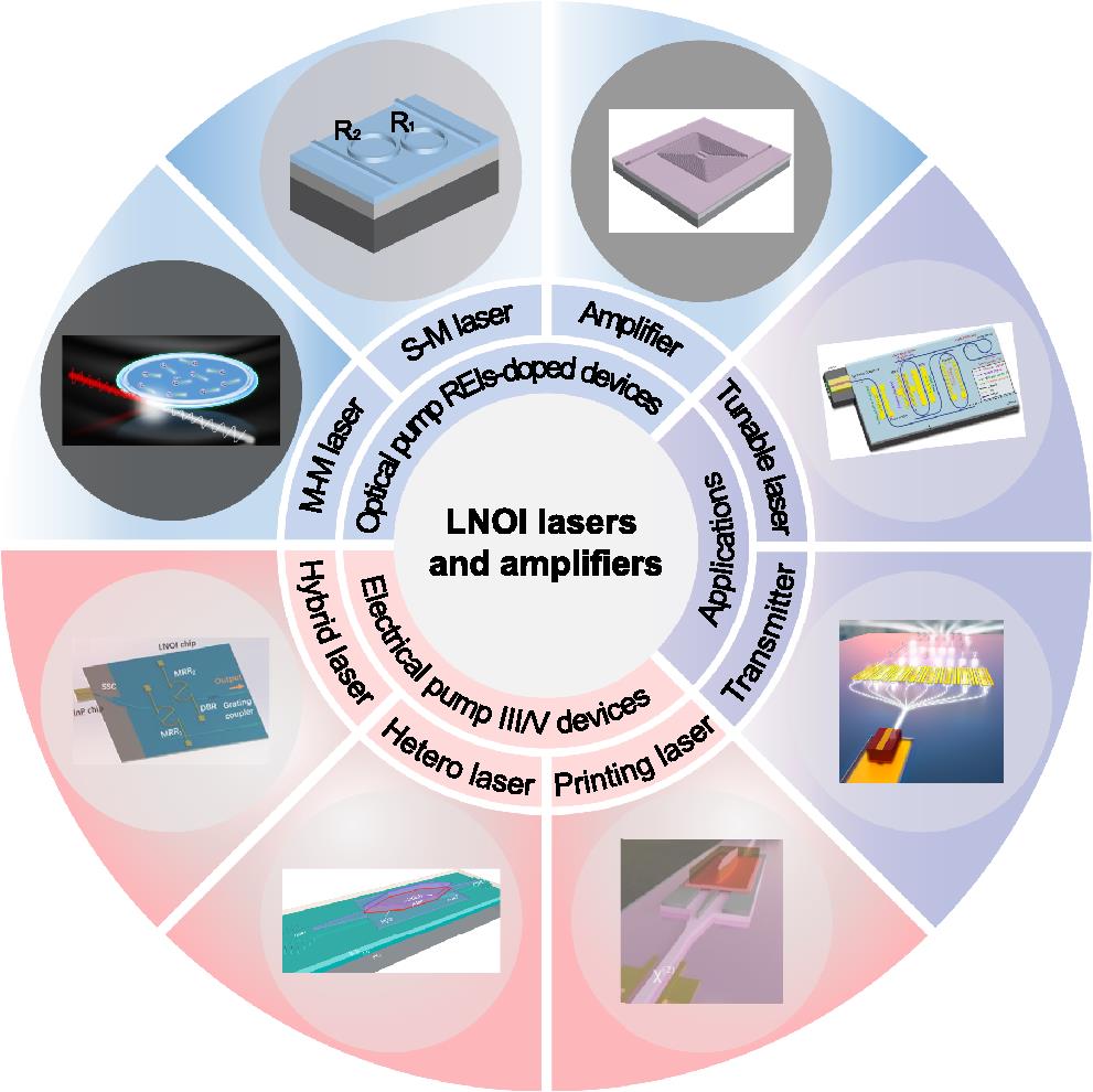
This paper reviews the recent research on lasers and amplifiers developed on the LNOI platform. Figure 1 shows the research road map for the LNOI light sources and amplifiers, which is also the overall idea of this paper. In Sec. 2, the research processes of lasers and amplifiers based on REI doping LN are introduced. Specifically, the common methods of REI doping in LN crystals and the study of spectral characteristics of doped crystals are discussed first. Subsequently, the important parameters for characterizing microlasers are discussed. Then, the research works of multimode microdisk lasers, multimode microring lasers, single-mode lasers, and amplifiers on the REI-doped LN thin film are presented. At the same time, the challenges of laser and amplifier performance and the potential improvement scheme for the REI-doped LNOI lasers and amplifiers are discussed. In Sec. 3, the electrically pumped III-V lasers and amplifiers on LNOI platform, as well as the applications of the laser transmitter and tunable Pockels laser confirmed by deploying the electro-optical effect of LN are introduced. Then, the advantages and challenges of the LNOI III-V lasers are analyzed with a comparison with REIs-doped lasers. In Sec. 4, the application prospects of LNOI-based lasers and amplifiers are explored, combined with other LNOI functional devices, such as sensing, broadband optical communication, and frequency converter. Finally, in Sec. 5, the contents of the whole review are briefly summarized. At the same time, future research and development of LNOI-based lasers and amplifiers are envisaged.
Sign up for Advanced Photonics TOC. Get the latest issue of Advanced Photonics delivered right to you!Sign up now
The indirect bandgap structure of LN crystal makes it challenging to realize electrically pumped luminescence. Nevertheless, photoluminescence based on REI doping is a simple and effective method that is widely favored by researchers. For example, various REI-doped waveguide lasers and amplifiers based on bulk LN crystal have been confirmed successfully.35–38 Combined with the advantages of strong mode localization and low transmission loss, active devices based on REI-doped LNOI platforms are expected to achieve better performance. In this section, the recent progress of REIs doping, spectroscopic analysis, microlasers, as well as amplifiers based on REIs-doped LNOI platforms is summarized.
2.1 Rare-Earth Ion Doping and Spectroscopic Analysis
Roughly, there are three main ways to dope REIs into LN crystal. The first one is to add REI oxide for doping when growing LN crystal by the Czochralski method and obtain LN single crystal with uniform ion concentration,39,40 as shown in Figs. 2(a) and 2(d). The second method is thermal diffusion, mainly through vacuum deposition of the REI layer, and then selective doping through high-temperature diffusion,37 as shown in Fig. 2(b). In thermal diffusion doping, the diffusion depth of REIs has the characteristics of from complementary error function (erfc)-like to semi-Gaussian shape distribution [Fig. 2(e)].41 Due to the low diffusion rate of REIs, the diffusion temperature must be close to the Curie temperature of LN, which is generally as high as 1100°C and requires a diffusion time of up to 150 h. The diffusion time depends on the crystal phase of the LN substrate. The third method is to dope LN crystals with REIs by ion implantation,42 as shown in Fig. 2(c). At room temperature, ions are accelerated to million electron volt energy by Van der Graaff accelerator or transistor accelerator and implanted into the LN crystal. The ion concentration displays a nearly Gaussian distribution [Fig. 2(f)] and high-temperature annealing above 1000°C is needed to eliminate the defects caused by implantation and restore the quality of single-crystal LN.
Figure 2.Methods for REI doping into LN crystal and the corresponding concentration-depth distribution. (a) and (d) Crystal growth doping; (b) and (e) thermal diffusing doping; and (c) and (f) ion implantation doping. , doping concentration and , the available maximum doping concentration for the corresponding method.
The above three doping methods are relatively mature technologies after a long time of development and are expected to realize industrialization. But they also have their advantages and disadvantages. For example, compared to diffusion and ion implantation doping, crystal growth doping can obtain a high doping concentration and more uniform ion distribution and thus has a promising future in realizing high power and low transmission loss lasers and amplifiers. In contrast, for thermal diffusion and ion implantation, the maximum concentration of doped erbium ions is 43 and (molar fractions; hereinafter percentages referring to doping concentrations represent molar fractions, unless specified otherwise),44 respectively, and the distribution of ions is erfc-like or Gaussian distribution, which has certain restrictions on the development of applications with high doping concentration, such as amplifiers. However, it has the ability of local doping for thermal diffusion and ion implantation doping, so it can flexibly control the doping region and avoid additional loss of passive devices on integrated optical chips and becomes an ideal scheme to build a locally doped optical gain chip.
In recent years, referring to the incorporation of REIs into LN bulk crystal, many research groups have carried out research on REI-doped LNOI integrated photonics.45,46 For example, Dutta et al. first prepared 300-nm-thick thin-film LN from 0.1% thulium-doped X-cut LN bulk by the smart-cut process, and then prepared the grating coupling structure and single-mode waveguide by EBL-dry etching process, as shown in Fig. 3(a).47 To explore the optical properties of thulium ions in the thin-film waveguide, the absorption, emission spectra, and fluorescence lifetime were measured at a 3.6 K low temperature. Compared to a thulium doped-bulk crystal, the thulium ions in smart-cut thin film displayed virtually identical optical properties, which indicates that the smart-cut process can preserve the optical properties of REIs in thin films well. Notably, the preparation of the REI-doped LNOI is compatible with wafer-scale integration, paving the way to achieve on-chip active photonics systems and applications. Furthermore, an atomic frequency comb memory was realized in thulium-doped LNOI waveguides by the same doping and fabrication process, and the storage spectrum bandwidth and optical storage time were up to 100 MHz and 250 ns, respectively.53
Recently, Wang et al. explored the optical coherence of the erbium-doped smart-cut LN thin film prepared from bulk erbium-doped LN. Experimentally, optical coherence time was obtained by fitting the exponential decay curve of the echo signal strength as a function of time delay.54 The coherence time, also referring to coherence lifetime, is a parameter to reflect the homogeneous broadening linewidth of the REI spectrum and thus indicates the ability of application for quantum information processing.55,56 The obtained coherence time is comparable with the value of bulk crystal, indicating that the erbium-doped smart-cut LN thin-film platform shows promise for developing on-chip quantum storage. At the same time, Rüter et al. characterized the spectral properties of a neodymium-doped LN thin film fabricated from an LN substrate diffusion-doped with neodymium ions before the smart-cut fabrication process and showed an opportunity to realize active gain areas with locally varying doping concentrations.57
In addition, Wang et al. also carried out research on ion implantation doping based on a prepared LNOI microcavity. First, a microring coupled with a waveguide was fabricated by the etching process. Then, erbium ions were doped by ion implantation with an implantation energy of 350 keV and a flux fluence of .48 The optical properties could be partially recovered and the average value of the microring cavity is after post-implantation annealing at 550°C for 5 h. The scanning electron microscope (SEM) image of the fabricated devices and the simulated ion density distribution are shown in Fig. 3(b). The fluorescence lifetime of erbium ion, defined as the time constant corresponding to the exponential decay of the ion from the energy level in the form of spontaneous emission or non-radiation reflecting the local environment of the ion, is measured as 3.2 ms at low temperatures. Such a fluorescence lifetime is higher than 2 ms in LN bulk crystal. Therefore, it reflects that there may be differences in the local environment of erbium ions, refractive index, and Li/Nb ratio of the material compared with the doped bulk LN.42 At the same time, the resonance-enhanced fluorescence decay caused by the coupling between ions and cavity was observed, which is referred to as the Purcell effect58,59 and is expected to develop high-efficiency light emitters.60 The enhance factor is defined as the Purcell factor and can be expressed as , where and are the quality factor and mode volume of microcavity resonance mode, respectively.59 In this work, the average Purcell factor was calculated as 3.8. In the same period, Pak et al. adopted a similar method to incorporate ytterbium ions into fabricated LNOI microring resonators and centimeter-long waveguides.49Figure 3(c) shows the schematic diagram of the ytterbium-doped LNOI waveguide structure and the simulation of implanted ytterbium ions distribution with a peak concentration of 0.0002%. The doped device was annealed at 500°C for 8 h under a nitrogen atmosphere to heal the lattice damage caused by ion implantation. The loaded of the microring was measured at at 908 nm. The photoluminescence characterization found that the lifetime of ytterbium ions on resonator pumping is shortened slightly compared to nonresonant pumping, which is attributed to the Purcell-enhanced emission with a Purcell factor of 0.45.
At the same time, Xia et al. directly doped ytterbium ions into an X-cut LN thin film with a thickness of 470 nm by ion implantation.50 After post-annealing at a slightly higher temperature of 650°C, no apparent film damage was observed. Then, ytterbium-doped microcavities with a radius of and a of were fabricated by EBL and chemical-mechanical etching protocol. A layer of indium tin oxide was deposited on the microcavity as an electrode to tune its resonant frequency electrically. The device schematic is shown in Fig. 3(d). Due to the ions-cavity coupling, the shortening of ytterbium ions’ lifetime was demonstrated with a Purcell factor of 10.24. The coupling between the REIs and microcavity based on electro-optic tuning can be controlled at switching speed over a 160 GHz range. In addition, the detection of a single ytterbium ion was carried out based on electro-optic dynamic tuning, which provides a platform for generating a deterministic single-photon source.
In addition, Yang et al. hybrid integrated the erbium-doped yttrium orthosilicate with a concentration of 50 ppm (parts per million) to LNOI microring by flip-chip bonding, as shown in Fig. 3(e).51 The fluorescence lifetime of erbium ions was measured as 11.5 ms, consistent with the bulk material result of 11.4 ms. At the same time, the resonance broadening phenomenon caused by ion-cavity coupling was also observed, and the coupling intensity factor was assessed to be 0.36. Moreover, the erbium ions-implanted LN crystal directly integrated on a silicon photonic chip was reported by Jiang et al., as shown in Fig. 3(f). The optical properties of erbium ions in the integrated structure were investigated, and a modification of the photoluminescent emission was observed.52
Affected by the differential thermal expansion rates of the layers in the LNOI wafer, the tolerable annealing temperature () of the LNOI wafer is far below the required temperature of for the thermal-diffusion and ion-implantation doping of REIs into LN bulk crystal. Therefore, the incorporation of REIs into the LNOI platform by ion implantation methods after the smart-cut process significantly limited the doping concentration and ion distribution and naturally limited the optical properties of REIs. Fortunately, incorporating REIs into the LNOI platform before the smart-cut process is feasible. Additionally, this method can preserve the desirable optical properties in bulk crystals and can be compatible with scalable planar fabrication. Xu et al. studied the refractive index, erbium ion spectrum, and other material properties of the erbium-doped LN film prepared based on the smart-cut process. They found that the material properties of the LN film are close to the erbium-doped bulk LN. This indicates that high-quality REIs-doped LN film can be obtained based on the smart-cut process.61 This provides a path for the realization of on-chip LNOI lasers and amplifiers by adjusting an appropriate doping concentration of the LN bulk sliced to a thin film. Thus, a series of groups have recently focused on realizing LNOI lasers and amplifiers based on REI-doped LN thin film.
2.2 Whispering Gallery Microcavity Lasers Based on REI-Doped LNOI
The three elements of a laser are the pump source, the gain medium, and the resonator. The gain medium and pump wavelength are determined by selecting the type of REI. The resonant cavity of a traditional laser is mainly composed of two or more mirrors. Compared with traditional resonators, whispering gallery mode (WGM) microcavities with circular structures can confine light by “continuous total internal reflection” for a long time within an ultrasmall mode volume, leading to strong light–matter interactions. Benefiting from the high quality factor () and small mode volume (), WGM microcavity is regarded as an ideal platform to realize ultralow threshold lasers with a small footprint and narrow linewidth.62–64 For example, Yang et al. reported an erbium-doped microlaser on a silicon chip with an ultralow threshold of 660 nW.65 In this section, some important parameters for the characterization of WGM lasers were first discussed in Sec. 2.2.1. Then the development status of multimode microdisk and microring lasers based on REI-doped LNOI was introduced in Sec. 2.2.2. Finally, the research progress of the single-mode lasers and development constraints for the REI-doped LNOI microlasers were analyzed in Sec. 2.2.3.
2.2.1 Important parameters for characterizing microlasers
Before introducing the research progress of microlasers based on REI-doped LNOI, we discuss some important parameters for characterizing microlaser performance.
Lasing threshold
The lasing threshold refers to the pump power when the gain provided by the gain medium is just equal to the loss of the laser cavity. The pump threshold power () of WGM microcavity laser can be approximately expressed as66where and refer to the effective refractive index and quality factor of the corresponding laser signal mode, respectively. and indicate the signal and pump wavelengths, respectively. is the mode volume of the pump mode, and is the pump efficiency. and refer to the Planck constant and the speed of light in vacuum, respectively. and respectively correspond to the stimulated emission cross section and fluorescence lifetime of the gain ions. As can be seen from Eq. (1), for a given gain medium, to obtain a low laser threshold, the effective way to reduce the laser threshold is to improve the pumping efficiency, increase the value of the resonator, and reduce the mode volume, which is also a significant advantage of conducting laser research based on WGM resonators. Specifically, high can be obtained by improving the processing technology. For example, the maximum value of an LNOI WGM cavity up to has been demonstrated based on an ion-free preparation of LN thin film, which is close to the upper limit of the intrinsic absorption of bulk LN and shows great potential in the application of ultralow threshold lasers.67 The mode volume can be reduced by reducing the size or thickness of the resonant cavity. However, it should be noted that too small a diameter or thickness may lead to increased radiation loss of the resonant cavity, and the balance between the and needs to be considered in the actual research to obtain a maximum value of . In addition, the optimization of pumping efficiency involves major factors such as the coupling between the tapered fiber (or waveguide) and the resonator, the overlap of the pump mode and signal mode in the gain medium, as well as the absorption of the gain medium to the pump.
Conversion efficiency and maximum laser output power
The conversion efficiency of a laser refers to the rate of change of the generated signal power relative to the pump power at the working stage above the lasing threshold, which reflects the conversion efficiency from the pump to signal during the laser operation. At the same time, it is obvious that the maximum laser output power refers to the maximum power that can be obtained when the laser is working, which can reflect the available power level of the laser for subsequent work. For optimizing these two parameters, laser signal extraction should also be optimized. That is to say, high pump efficiency and signal extraction efficiency should be guaranteed simultaneously. However, because the pump and signal are in different bands, the coupling state between a tapered fiber or straight waveguide and a resonator is inconsistent. Generally, the maximum output power of the laser is observed when the pump light is in an overcoupled regime in the experiment. To realize high conversion efficiency and low threshold, it is often necessary to design a broadband coupling to meet the requirements of efficient pump and signal extraction.68 In addition, different from optimizing the laser threshold, a large resonator size or cavity length is required to improve the gain accumulation to obtain an intense laser output.
Laser linewidth
Laser linewidth usually refers to the full width at half-height of the signal mode in the laser spectrum, which is an important parameter reflecting the coherence and noise of the laser. According to the Haken–Lax–Scully formula, the linewidth of the emitted laser operating above the threshold can be expressed as69where is the Planck constant, and are the emitted frequency and power of the laser, respectively, and is the linewidth of the cavity mode. Increasing the resonator’s quality factor and output power is an effective way to reduce the linewidth of the laser. The discussion of other factors affecting laser performance, such as doping concentration, can be found in the previous review on WGM microcavity lasers.63 Then, the research progress of multimode microdisk lasers, multimode microring lasers, and single-mode microlasers based on REI doped-LNOI platform is introduced in the following sections.
2.2.2 Multimode microdisk and microring lasers
Wang et al. reported an erbium-doped LNOI laser based on a -diameter microdisk fabricated on an erbium-doped chip with a doping concentration of 1% by the PLACE process.70 The factor was measured to be at 1563 nm by the scanning transmission spectrum method. The emitted laser signal at the 1560-nm band and the accompanying strong green-up conversion fluorescence were observed under the 976-nm laser pump, as shown in Fig. 4(a). The threshold of the laser signal was lower than , and the conversion efficiency was deduced as by fitting the signal power data. In addition, the blue-shift (red-shift) of the signal wavelength at a lower (higher) pump power with a rate of () was observed. The possible reason for this shift process is that the photorefractive and thermo-optical effects of LN exist together, and the photorefractive effect is dominant at low pump power, while the thermo-optical effect dominates at high power.
Subsequently, Liu et al. fabricated a -diameter microdisk by the focused ion milling process based on an erbium-doped LNOI wafer with a doping concentration of 1%.27 The laser emission at 1550-nm band with a linewidth of was observed under the laser pumping at 974 and 1460 nm, respectively. Due to the thermal effect of the LN microdisk, the redshift processes of the emission signal wavelength were observed when increasing the pump power for both pump bands, and better thermal stability was obtained at a 1460-nm pump. The threshold for the 974-nm pump was measured as 2.99 mW with a conversion efficiency of . At the same time, Luo et al. reported the batch preparation of erbium-doped LNOI microdisk lasers using etching and an additional chemo-mechanical polishing (CMP) process.71 The threshold and conversion efficiency of the dominant signal mode in the 1530-nm band were deduced as and , respectively, as shown in Fig. 4(c).
Except for the 1550-nm band, the microlaser operating at other wavelength bands has many unique applications. For example, due to the negligible water absorption at the 1060-nm band, the ytterbium ion emission can be applied for biosensing. In addition, compared with an erbium ion, ytterbium ion has a simple energy level structure and higher absorption cross section at the 980-nm band, which has substantial potential to improve the output power and conversion efficiency of microlasers. Zhou et al. first reported a microdisk laser based on an ytterbium-doped LNOI chip.72 With the continuous laser pump at 984 nm, the lasing signals at the 1030- and 1060-nm bands were observed in the increasing pump power range, as shown in Fig. 4(d). A threshold of and a conversion efficiency of 0.53% for the collected signal laser were derived by linearly fitting the signal power data at the different pump powers. Compared to the erbium-doped LNOI microlaser, the conversion efficiency has been significantly improved due to the high quantum efficiency of ytterbium ions.74–76 Meanwhile, due to the strong nonlinearity of LN, the second-harmonic generation (SHG) of the pump laser and the sum frequency generation (SFG) between the pump and emission signal were also observed, as shown in Fig. 4(e).
Subsequently, Luo et al. also reported 1060-nm band microdisk lasers with a high conversion efficiency.73 Based on an ytterbium-doped LNOI wafer with a doping concentration of 1.5%, the microdisk cavities were fabricated in a batch using etching and the CMP process. The loaded factors at 970.20 and 1502.68 nm were measured as and , respectively. With a 980-nm band laser pump, the emission signal at the 1060-nm band was detected by OSA. The blueshift phenomenon of the signal mode wavelength at a rate was observed under the increase of pump power due to the photorefractive effect of the LN crystal. The power and linewidth of the dominant signal mode under different pump powers are shown in Fig. 4(f). An S-shaped curve for the pump-power-dependent signal power was observed, which indicates that the collected signal belongs to a lasing signal. The threshold and conversion efficiency were deduced as and 1.36%, respectively. Benefiting from the high doping concentration and high factors of the fabricated microdisk, as well as the effective signal extraction, the conversion efficiency is the highest value for the reported REI-doped LNOI microlasers. This work significantly improved the microlaser performance and shows the potential of the LNOI platform in biosensing applications.
The research works of REI-doped LNOI laser described above are based on microdisk cavities. The microdisk cavity is mainly pumped and monitored by a fiber taper, which has the limitations of unstable coupling and inconvenient further integration with other on-chip functional devices. Microring cavities coupled with an on-chip waveguide can overcome these limitations. Furthermore, microring cavities usually have a smaller mode volume than a microdisk cavity with the same radius, which means that the light field power density in the cavity is more significant under the same pump power, leading to a lower laser threshold.
Luo et al. prepared a microring cavity coupled with a waveguide using the etching technique on a Z-cut erbium-doped LNOI wafer with a doping concentration of 0.1%.77 The loaded at 1531.8 nm was measured as (intrinsic ), corresponding to a waveguide loss of . Under the 980-nm band continuous laser pump, lasing emission was realized in the 1530-nm band. The lasing threshold was estimated to be , and the conversion efficiency was deduced as by linearly fitting the signal mode power data, as shown in Fig. 5(a). Benefiting from the small mode volume and high optical power density of the microring structure, the achieved threshold is reduced by 1 order of magnitude compared with the erbium-doped microdisk laser. Till now, is the lowest lasing threshold based on the reported REI-doped LNOI microlasers.
At the same time, Yin et al. fabricated a Z-cut erbium-doped LNOI microring cavity with 1% doping concentration and an undoped LNOI waveguide by the PLACE technique, respectively. Then, the LNOI microring was vertically coupled with the waveguide structure, as shown in the inset of Fig. 5(b).78 With a 980-nm laser pump, a broadband lasing signal in the 1550-nm band was observed with different pump power. A lasing threshold of 3 mW was deduced by fitting the signal power data. The wavelength tuning of the mode around 1533 nm was electrically tuned in a range of 0.2 nm with an EO coefficient of , as shown in Fig. 5(c), by applying an external voltage to the electrodes integrated with the racetrack microcavity.
In addition, an integrated ytterbium-doped LNOI microring laser working at 1060-nm band was recently demonstrated by Luo et al.79 Similar to the reported erbium-doped microring laser,77 the microring was fabricated using the etching technique on an ytterbium-doped LNOI wafer with a 1.5% doping concentration. In experiments, the multi-peaks in the range of 1056 to 1066 nm were observed when the pump wavelength tuned into the microring resonance mode, as shown in Fig. 5(d). The maximum signal power was up to at 1060.49 nm, which is a great improvement compared with the previously reported erbium-doped LNOI microlaser. The signal power and linewidth of the dominant mode were recorded while increasing pump power, as shown in Fig. 5(e). By fitting the linear increase portion of signal power, the threshold and conversion efficiency were deduced as and , respectively. A higher conversion efficiency is expected to improve the pump efficiency and signal extraction efficiency by introducing the pulley waveguide coupling design. Due to the integrated feature and stable performance of microring cavities, these microring lasers may find more practical applications.
2.2.3 Single-mode lasers
Due to the broadband gain property of REIs, the REI-doped LNOI microcavity lasers introduced above generally operate in a multimode state, which is subject to false signals, random fluctuations, and instabilities and thus limits its application scenarios. Therefore, single-mode lasers featuring monochromaticity, high stability, and controllable output wavelength have attracted much attention due to their great potential for practical applications, such as optical communication and optical sensing. At present, there are four main ways to realize a single-mode laser. (1) Decreasing the size of the cavity to enlarge the free spectral range (FSR) and ensure only one resonant mode in the gain band range. (2) Designing narrowband distributed Bragg reflector (DBR) or distributed feedback (DFB) structures in the resonance cavity to achieve mode selection. (3) Cascading two or more cavities to realize mode selection by the Vernier effect. The specific mechanism is that the subcavities with different FSR (size) are coupled together. In such a system, the “supermode” is formed in the coupled cavities at the resonance overlapping location, while other normal modes resonate in only one cavity and dissipate in another cavity, resulting in greater losses. Therefore, the supermode with enlarged FSR and higher values can be selected. Combined with the gain competition between the modes in the gain band, the single-mode operation of the laser can be realized. (4) Spatially selective pumping to suppress high-order mode gain or controlling mode loss to achieve single-mode lasing. Among them, reducing resonator size will increase the radiation loss of the light field in the cavity and thus increase the threshold power density of the laser, so this scheme is less commonly used. The following part will introduce the research progress of single-mode laser based on the REI-doped LNOI platform.
First, Gao et al. fabricated coupled microdisks, also referred to as photonic molecule, based on erbium-doped LNOI with 1% doping concentration using the PLACE technique.80 The coupled microdisks with a diameter of 29.8 and , respectively, are separated by a gap of . Under the 977.7-nm laser pump, the single-mode laser emission at 1550.5 nm with a threshold of was realized using the inverse Vernier effect, as shown in the spectra in Fig. 6(a). It is worth noting that the pump was resonant in both microdisks, and the signal was mainly localized in the small microdisk when the single-mode laser was working. In addition, a minimum signal linewidth of 348 kHz was characterized using a Michelson interferometer composed of an optical fiber coupler to measure the laser frequency and phase noise.
Subsequently, to effectively improve the integration and scalability of REI-doped LNOI single-mode lasers, Zhang et al. designed a microring photonic molecule with radii of 85 and to achieve a single-mode laser, as shown in the inset of Fig. 6(b).28 The photonic molecule was fabricated by the etching process based on an X-cut erbium-doped LNOI chip with 0.1% doping concentration. In experiments, the double resonance at 1531.6 nm for the two microring cavities was confirmed by the transmission spectra. Moreover, the FSR of the supermodes of the photonic molecule was enlarged to 11 nm in the 1550-nm band due to the Vernier effect. At the same time, the nonsupermodes were also observed in the transmission spectrum, which have a lower coupling depth due to a greater loss and thus a higher lasing threshold. As a result, the single-mode laser was achieved in the supermodes. Figure 6(b) shows the collected emission signal spectra at a pump power of showing a side-mode suppression ratio (SMSR) of up to 26.3 dB. The threshold was estimated as by analyzing the signal power with the increasing pump power.
Soon afterward, to reduce the requirement of tunability of pump light, Liu et al. demonstrated an erbium-doped LNOI single-mode laser based on a photonic molecule with a microdisk and a microring, as shown in the inset of Fig. 6(c).81 In this device, a single-mode laser emission with an SMSR of 31.4 dB in the range of 1520 to 1570 nm was observed with a 974-nm LD light source pump. Figure 6(c) displays the collected single-mode laser power as a function of pump power. The threshold and slope efficiency were deduced as 1.31 mW and , respectively. Moreover, the dependence of output power and wavelength on temperature was also investigated. With the increase in temperature, the output power increment and signal wavelength redshift were observed, which may be due to the change of cavity mode resonance state caused by the thermal-optic effect of LN.
During the same period, Xiao et al. designed a single-frequency erbium-doped LNOI laser based on a coupling structure composed of a short microring cavity with a diameter of and a long cavity with a length of 1.2 cm.82Figure 6(d) depicts the schematic diagram of coupling structure and the operation principle of single-frequency laser. The FSRs of the two cavities are and , respectively. Based on the Vernier effect, only the frequency located in the gain bandwidth and resonated on both cavities can oscillate. With a 1484-nm laser pump, a single-frequency laser emission near 1531 nm with an SMSR of 31 dB was observed, as shown in Fig. 6(e). The linewidth of the obtained single-frequency laser was detected as 1.2 MHz through a self-heterodyne method. A threshold of 13.54 mW and a slope efficiency of were measured as well. The reason for a relatively high threshold may be using a broadband source (0.5 nm) as the pump.
Actually, controlling mode loss is also a popular way to achieve single-mode lasing due to the compact device size. For example, Li et al. demonstrated a single-mode laser based on a single microring resonator by regulating the mode loss.83 The microring resonator with a pulley waveguide was fabricated on a Z-cut 1% doped erbium-doped LNOI wafer using the etching process. Based on simulation analysis, the supported four modes (, , , and ) on the -wide microring are shown in Fig. 7(a). Compared to mode , other modes (, , and ) have large mode areas and overlap with the rough sidewall and thus undergo a higher scattering loss. As a result, except for the mode, the gain of the other modes was effectively suppressed. In the experiment, the designed single microring realized single-mode lasing at with a 35.5-dB SMSR under the 1484-nm laser source pump with the assistance of the gain competition, as shown in Fig. 7(b). The lasing signal power is up to , and a threshold of 14.5 mW and a conversion efficiency of were inferred by linearly fitting the signal power data. In addition, the wavelength shift with the increasing pump power caused by the photorefractive effect was also observed. The linewidth of the single-frequency laser was measured as 0.9 MHz by a self-heterodyne approach.
Further, Lin et al. realized a single-frequency ultranarrow linewidth laser on a single microdisk, taking advantage of the polygon modes with high-quality factors and sparse mode distribution.84 The microdisk with a diameter of was prepared on a Z-cut 1% erbium-doped LNOI wafer. In experiments, the polygon modes for both pump () and signal (1550-nm band) were excited by adjusting the coupled tapered fiber to a proper position, as shown in the inset of Fig. 7(c). Because the signal polygon mode has a large FSR (11.5 nm) and overlaps with the pump polygon mode, the gain of the conventional high-density WGMs was effectively suppressed. Accordingly, the single-frequency lasing with a threshold of and a maximum SMSR of 37 dB was achieved in the gain band of erbium ions, as shown in Fig. 7(c). The output power of up to was obtained at a pump power of 20 mW. The microlaser linewidth was assessed as low as 322 Hz by heterodyning two separately pumped single-mode microlasers. Moreover, a microelectrode with a radius of was fabricated on the microdisk to investigate the wavelength tuning using the strong electro-optic effect of LN. As shown in Fig. 7(d), a linear tuning efficiency of was achieved when the applied voltage was tuned from to 300 V. The demonstrated ultranarrow linewidth microlaser would facilitate highly coherent applications based on an LNOI integrated platform.
In addition, Liang et al. also demonstrated a single-frequency microlaser based on an erbium-doped LNOI microring with the shape of quarter Bezier curves.85 The signal spectra in the wavelength range of 1500 to 1600 nm with a single-frequency lasing were recorded with the increasing pump power of a 976-nm laser, as shown in Fig. 7(e). The reason for realizing single-frequency lasing was probably mode-dependent loss and gain competition by comparing the transmission spectrum of the microring and the amplified spontaneous emission (ASE) spectrum in the waveguide. For a similar mechanism, Zhu et al. observed a single-frequency lasing with an SMSR of 29.12 dB based on an electro-optically tunable erbium-doped LNOI microdisk, as shown in Fig. 7(f).86 In addition, the wavelength of lasing mode was realized through continuous tuning in a 45 pm range by applying the electric voltage from to 200 V.
With the continuous attention and efforts of researchers, microdisks, microrings, and microdisk-microring coupling lasers have been realized based on the REI-doped LNOI platform, and the working state of the laser has also been improved from multimode to single mode. Table 1 summarizes the main performance parameters of the REI-doped LNOI microlasers reported so far. Based on the current research results, we discuss the main limitations and potential solutions for the development of REI-doped LNOI lasers.
Devices
Pump
Signal
References
Wavelength (nm)
Threshold ()
Wavelength (nm)
Power (nW)
Linewidth
Conversion efficiency
Modes or SMSR (dB)
Disk
974
1531.6
0.12 nm
Multiple
27
1460
1531.6
0.14 nm
Multiple
Disk
976
<400
1563.3
0.024 nm
Multiple
70
Disk
974
292
1531.8
Multiple
71
Disk
984
103
—
Multiple
72
Disk
21.19
Multiple
73
Ring
974
1532.4
Multiple
77
Ring
∼980
—
Multiple
78
Ring
974
59.32
Multiple
79
Coupled disk
977.7
1550.5
348 kHz
Single
80
Coupled ring
979.6
1531.1
—
26.3
28
Coupled ring
1484
1531
1.2 MHz
31
82
Ring
1484
14.5
1531.3
1.27 MHz
35.5
83
Disk
968
1546
322 Hz
37
84
Coupled disk and ring
974
1560.4
—
31.4
81
Ring
976
1530.9
0.045 nm
85
Disk
976
—
1544.7
—
—
29.12
86
Disk
980
485.5
1551.68
0.11 MHz
—
87
Sagnac reflector
980
1544
28 pm
25
88
Table 1. Typical parameters comparison of reported REI-doped LNOI lasersa.
Low output power (μW-level) and conversion efficiency
At present, the conversion efficiency and output power of the reported lasers are still at a relatively low level of microwatts in either multimode or single-mode operation, which hinders the further integration of the laser with other functional devices. We believe that there are several ideas to improve the output power of lasers. (i) Increase the scale of the resonator. The reported works are based on WGM microcavities with a micrometer-scale radius, which limits the optical gain of the laser within such a small gain volume. Therefore, expanding the scale of the gain resonator is a promising method to improve the laser output power. For example, a high laser output power based on large-sized microdisk cavities87 and long waveguides with Sagnac loop reflectors88 has been reported recently. Compared with previous work of REI-doped LNOI microlasers, the output power has been improved by an order of magnitude. It should be noted that increasing the cavity length will naturally bring about the impact of multimode resonance, which poses a challenge to the single-mode operation of the laser. The mode screening mechanism for realizing single-mode operation described above needs to be considered in laser design. At the same time, the optimization of coupling between the bus waveguide (or tapered fiber) and resonant cavity for both pump and signal bands, such as introducing the bending waveguide coupling design68 to ensure effective pumping and effective extraction of signal light, can also effectively improve the output power and conversion efficiency of the laser. In addition, the waveguide integrated with the Bragg grating resonance structure can effectively increase the cavity length and ensure single-mode operation. The DBR or DFB laser with high output power has been confirmed on the silicon-based integrated photonics platform,89–91 which can provide a reference for improving the laser performance. (ii) Introduction of cladding pumping scheme. Referring to the development of fiber lasers, the design of the cladding pump can effectively improve the pump efficiency of high-power diodes and ensure the single-mode operation of signal light, which plays a key role in developing the high-power fiber lasers.92,93 Similarly, based on the LN REI gain platform, coating the gain device with appropriate cladding layers, such as silicon dioxide and silicon nitride, can also improve the pump power in the gain structure. Unlike the optical fiber structure, the waveguide is not a circular symmetric structure and may need a reasonable design to ensure the adequate overlap of the pump light and the gain ions. (iii) Co-doped ytterbium ions. For erbium-doped fiber lasers working in the communication band, co-doped ytterbium ions are often used to increase the output power of the laser.94,95 This is because ytterbium ions, as a sensitizer, can effectively transfer energy to erbium ions, improving the luminous efficiency of erbium ions. At the same time, for the LN thin-film platform, erbium and ytterbium ions can be conveniently co-doped in the incorporation process of REIs, so it is expected to improve the output power and conversion efficiency of erbium-doped LN thin-film laser.
Optical pumping scheme
Due to the selection of REIs as the gain medium, the working mechanism of optical pumping for the lasers is necessary, which imposes limitations on using lasers for out-of-laboratory applications, such as gas detection and biosensing. A practical solution is to integrate a commercial semiconductor laser as the pump source for the LNOI laser. For example, the electrically pumped laser and REI-doped chip can be hybrid integrated by the flip-chip technology, which is expected to effectively improve the portability of the laser. Zhou et al. reported the pioneering work demonstrating the electrically pumped REI-doped LNOI laser for the first time by butt-coupling a laser diode chip with an erbium-doped LN gain chip.96 In addition, the electrically pumped REI-doped LN lasers can also be realized by heterogeneously integrating III-V materials on REI-doped LN chips to construct the pump laser.97 It should be mentioned that compared with the electric pump laser realized by direct hybrid integration or heterogeneous integration, REIs have a long excited-state lifetime, resulting in REI-doped LNOI lasers with low signal noise and narrow linewidth, which has advantages for developing applications, such as optical coherent communication and quantum optics.
Wafer global doping
As mentioned in the previous introduction, the LN thin film cannot tolerate the high temperature conditions required by thermal diffusion or ion implantation to achieve high-concentration doping. Therefore, the method of incorporating REIs into LN thin film for the currently reported REI-doped microlasers is mainly doping in the growth process of bulk LN before ion slicing. However, one of the side effects of this doping method is that REIs are distributed on the entire LN thin-film wafer, which brings additional absorption loss and refractive index changes to the passive device integrated on the same chip, degenerating the device’s performance. There are several ways to realize local doping. (i) Before the LN thin film is formed by ion slicing, bulk LN wafers can be doped locally with REIs by thermal diffusion or ion implantation. Rüter et al. prepared a neodymium-doped LN thin film by thermal diffusion doping before ion slicing, which confirmed the possibility of local doping by this method.57 At the same time, it should be noted that incorporating REIs by thermal diffusion or ion implantation may pose a challenge to the sliced thin film quality. For example, Xu et al. reported that the thermal diffusion doping process increases the roughness and causes a slight deformation at the diffusion surface of the erbium-doped LN wafer.61 An additional CMP step before the ion slicing process is expected to improve this diffusion surface quality. (ii) Integrated REIs-doped LN thin film with undoped LN thin film by butt-coupling to construct active-passive LN thin-film devices. For example, Zhou et al. reported the work of tiling erbium-doped LN film and undoped LN film with ultraviolet curing adhesive and then prepared the monolithically integrated amplifier using a single continuous photolithography process based on the active-passive chip.98 The limitation of this method is that due to the integration of two different chips, the thickness may vary, resulting in an additional loss at the optical interface of active and passive chips. At the same time, the scalability and stability of large-scale integration for this method have certain limitations due to splicing the two independent chips. (iii) Hybrid REI material on LN thin film. Another promising scheme for localized incorporation of REIs is to deposit materials locally with REI gain media on LN thin film. For example, REI-doped and REI-doped materials were widely used in active integrated photonics for their high rare-earth solubility, large emission cross section, as well as wafer-level deposition techniques.99,100 One consideration in this design is that sufficient overlap between the pattern of the LN layer and the gain material is required to obtain large gains or power output, for example, by depositing the gain material into the microtrenches design to improve the gain performance of the device.101,102 In addition, by introducing the design of REI-doped loaded waveguide, the fabrication process of active devices based on LNOI can be simplified. For example, silicon nitride materials featuring low transmission loss, refractive index close to LN, and CMOS compatibility are successfully applied on the LNOI platform.103,104
Some other aspects still need to be explored. The locking of the pump mode and the encapsulation of the coupling region deserve to be explored in the experiment to obtain high output power and stable operation of the laser during high-power pumping. Moreover, the wavelength tunability of the reported single-mode lasers is also limited. The thermo-optic effect of LN crystal can be utilized to achieve broadband wavelength tuning by integrating microheaters on the coupled resonators.105 Furthermore, combined with the outstanding electro-optical properties of LN, the REI-doped LNOI laser provides a promising platform for fundamental physics research, such as PT-symmetry breaking with natural advantages.106,107
2.3 Amplifiers Based on REI-Doped LNOI
In addition to lasers, amplifiers can provide gain for on-chip signals and therefore have fairly broad-based demand in on-chip optical communication, nonlinear frequency conversion, and other applications. High-gain waveguide amplifiers based on silicon nitride and integrated silicon platforms have been proven to be successful.108,109 However, due to the weak optical confinement as well as nonuniform distribution of REIs in titanium-diffused channel waveguide, the gain performance of waveguide amplifiers based on bulk LN is generally low ().110 Fortunately, as mentioned above, waveguides prepared based on REI-doped LNOI can obtain strong mode localization and high doping concentration with uniform distribution, which lays the foundation for the realization of large-scale integrated high-gain LNOI waveguide amplifiers. Consequently, the research on REIs-doped LNOI amplifiers has also attracted the attention of researchers.
Zhou et al. demonstrated the first waveguide amplifier on a Z-cut 600 nm-thick erbium-doped LNOI chip with 1% doping concentration.111 The 3.6-cm-long waveguide amplifier with a spiral design to reduce the overall device size was fabricated by the PLACE process. The signal gain at 1530 nm under different pump power was measured with a fixed on-chip signal power of 19.64 nW by a bi-directional pumping scheme. Then, considering the propagation loss calibration, the internal net gain for this signal wavelength was obtained by the equation where and are the measured signal powers in pump-on and pump-off state and and denote the transmission loss coefficient at the signal wavelength and the corresponding waveguide length, respectively. As shown in Fig. 8(a), the internal net gain exhibits a rapid rising stage (small-signal gain) and a gradual trend to gain saturation process following the growing pump power. A maximum internal net gain of 18 dB was achieved at the pump power of . At the same time, the strong green upconversion fluorescence in the waveguide was observed when the amplifier is operating, as shown in the inset of Fig. 8(a), which was investigated by Jia et al., who found a dual-color upconversion luminescence emission.116 The signal gain at different wavelengths was measured and consistent with the signal fluorescence spectrum, as shown in Fig. 8(b). In addition, the polarization dependence of amplifier gain was studied under different polarization states for both pump and signal modes. As a result, the maximum gain was obtained where pump and signal modes all have a TE polarization. This probably is due to that the TE modes in Z-cut erbium-doped waveguide have better absorption and emission cross sections for the pump at the 980-nm band and signal at the 1550-nm band, respectively. At the same time, the low transmission loss for TE polarization also contributes to obtaining a high gain. Additionally, the same group recently demonstrated a four-channel erbium-doped waveguide amplifier with a net gain of at 1530 nm based on a monolithically integrated active-passive LNOI chip.98
At the same time, Chen et al. fabricated a compact 5-mm-long waveguide amplifier using the etching and CMP process based on an erbium-doped LNOI with 0.5% doping concentration.112 Under the 980-nm laser source pump, the measured signal spectra for the increasing pump power in the range of 0 to 21 mW are shown in Fig. 8(c). The maximum internal gain at 1531.6 nm is about 5.2 dB, corresponding to a net gain per unit length of . The internal conversion efficiency was deduced up to 0.2% with the equation , where is the pump power. In addition, they also demonstrated a 4.3-mm-long erbium-doped LNOI waveguide amplifier with a signal enhancement factor of at a low pump power of 3 mW.61
Subsequently, Luo et al. reported on-chip erbium-doped LNOI waveguide amplifiers based on a similar simplified fabrication process without Cr film deposition and CMP steps.113 The amplifiers consist of a compact straight waveguide with a length of 5 mm. The doping concentration of erbium ions is 0.1%, which is much lower than that in previous reports. Under the 974.3-nm laser pump, the net internal gain at 1531.5 nm with a fixed signal power of 5 nW was investigated by increasing the pump power. A maximum net internal gain of 5.5 dB was obtained at a higher pump power of . In addition, the gain dependence on the signal power at 1531.5 nm with a fixed pump power (23 mW) was measured and is shown in Fig. 8(d). What is more, a maximum internal net gain of 15 dB at signal power is achieved. The internal net gain per unit length is up to , which is the highest value for the reported REI-doped LNOI waveguide amplifiers. It should be mentioned that the optimal gain is obtained under a weak signal power (), so the amplifier may be more suitable for small signal amplification, sensing, and other related fields.
To enhance the integration density of devices, Yan et al. also fabricated a 1% erbium-doped LNOI waveguide amplifier with a spiral design using the etching process.29 The waveguide has a total length of 5.3 mm with a footprint of . To characterize the spiral waveguide amplifier net gain, two lasers operating at 974 nm were used for the bi-directional pump. A maximum net gain of 8.3 dB at 1530 nm was obtained, which is considered equivalent to a net gain per unit length of . At the same time, the net internal gain in the 1520 to 1570 nm range was characterized and showed that the majority wavelength range could obtain an over 3 dB net gain.
In addition, inspired by the design of double-cladding fiber, Liang et al. fabricated -long tantalum pentoxide ()-clad erbium-doped LNOI waveguide amplifiers by depositing a -thick layer of on the top of LN waveguide core, as shown in the inset of Fig. 8(e).114 As part of the optical power in the LN core is introduced into the cladding waveguide, the detrimental absorption of pump power and signal powers by quenching ions is reduced. The optical gain of the waveguide amplifiers with -cladding was measured and shown to be superior to the amplifiers without cladding, with a maximum net gain of more than 20 dB at 1532 nm, as shown in Fig. 8(e). Recently, ytterbium-doped LNOI waveguide amplifiers fabricated by the PLACE process were reported by the same group.115 The maximum net gain at 1060 nm for a 4-cm-long waveguide [the inset of Fig. 8(f)] pumped by a 976-nm laser was measured at about 5 dB, as shown in Fig. 8(f).
Also, the influencing factors, such as pump wavelength, pump mode, and waveguide length for the performance of the amplifier were carefully investigated by Cai et al. based on an erbium-doped LNOI waveguide amplifier with a concentration of .117 An internal net gain of 16 dB at 1531.6 nm with a saturation power of was achieved on a 2.5-cm-long waveguide, as shown in Fig. 9(a). The amplifier noise figure mainly originates from spontaneous emission and shows a trend of increasing with the signal power. Experimentally, the minimal noise figure of 4.49 dB at signal power and near 6 dB in the range of signal power from to was observed, as shown in Fig. 9(b). In addition, the power conversion efficiency reflecting the pump effectiveness was characterized and displayed a trend of decreasing with the increasing signal power due to the reduction of the obtained internal gain, as shown in Fig. 9(c). Moreover, although the absorption coefficient of erbium ions in the 980-nm band is higher than 1480-nm band,118 the amplifier operating on the 1484-nm pump exhibits a higher gain than on the 980-nm pump, as shown in Fig. 9(d), which is mainly because the 1484-nm pump has a better overlap factor with signal and a lower transmission loss. The gain performance for different waveguide lengths was also studied, as shown in Fig. 9(e). The optimal length of 2.58 cm close to the simulation value of 2.68 cm was observed. Additionally, the pumping scheme was also studied in this work. Specifically, for forward pumping, the pump power is high at the front end and low at the back end, while the signal is opposite. Thus, for an amplifier with a long waveguide length or high doping concentration, when the signal light is transmitted to the back end, the remaining pump power is insufficient to provide sufficient gain, resulting in overall gain performance degradation. Although backward pumping can be applied to avoid the power distribution mismatch and obtain a greater gain, this pumping scheme will introduce a higher noise. Therefore, bi-directional pumping is often used to balance gain and noise performance. As shown in Fig. 9(f), a better gain and noise performance was obtained at the bi-directional pumping scheme compared to forward pumping and backward pumping.
As can be seen from the above introduction, amplifiers with straight and spiral oxide cladding waveguide structures have been successfully verified based on REI-doped LNOI platforms. The pumping wavelength and pumping scheme of amplifiers are also explored. Table 2 summarizes the key parameters of REI-doped LNOI waveguide amplifiers reported so far. However, there are still several problems that need to be resolved in the development of amplifiers, as discussed below.
Waveguide
Pump
Signal
Ref.
Length (cm)
Doping concentration (%)
Wavelength (nm)
Power (mW)
Pumping schemesb
Wavelength (nm)
Power (dBm)
Internal net gain (dB)
Gain per unit length (dB/cm)
Output power (dBm)
3.6
1
980
40
Bi
1530
−47.
18
5
−29.07
111
26
Bi
1550
−38.38
7.5
2.08
−30.88
0.5
0.5
980
21
For
1531.6
−50.86
5.2
10.4
−45.66
112
21
For
1550
−52.37
1.8
3.6
−50.57
0.5
0.1
974
∼23
For
1531.5
−65
15
30
−50
113
0.53
1
980
10.78
Bi
1530
−10.7
8.3
15.66
−2.4
29
2.8
1
980
45
For
1531.6
—
8.45
3.02
—
119
2.58
1
1484
17.31
Bi
1531.6
−50
16
6.20
−34
117
1484
18.54
Bi
1550
−50
2.66
1.03
−47.34
10
1
976
63
Bi
1532
−22
20
2
−2
114
4
0.5
976
16
For
1030
—
5
1.25
—
115
976
48
For
1060
—
8
2
—
2
—
976
14
For
1530
—
8
4
—
98
1550
—
5
2.5
—
Table 2. Typical parameters comparison of reported REI-doped LNOI amplifiersa.
Although a maximum net gain factor of 20 dB was realized based on a 10-cm-long waveguide. The high gain of the amplifier is obtained at the low input signal power (), which leads to the low output power of the amplifier and limits the application scenarios of the amplifier to a certain extent. To further improve the gain performance of the amplifier, especially for high signal power amplification, the most important problem to be solved is to reduce the propagation loss of the waveguide, which limits the available REI-doped waveguide length and, therefore, the attainable output power level.120 For example, a promising reference work is that Liu et al. achieved a signal output power of 145 mW with a signal input power of 2.61 mW based on a 0.21-m-long erbium-doped silicon nitride waveguide with a doping concentration of .121 The propagation loss based on this silicon nitride platform is , which is far lower than the reported value of LNOI erbium-doped amplifiers (an optimal value of ).111 Therefore, it is expected to obtain higher output power on a longer REI-doped waveguide by improving the processing technology. Moreover, the REI doping concentration and the mode overlap factor between the optical mode and REIs can be further optimized for more significant gain. In addition, for the amplification of high signal power, the coupling of the on-chip waveguide and off-chip pump is also a special concern. Due to the long REI-doped waveguide and high input signal power, higher requirements for on-chip pump power are also put forward. Therefore, it is necessary to introduce a high-efficiency coupler in the pump band or adopt a multichannel pumping scheme to meet the pump power requirement of the amplifier and avoid degradation of amplifier performance. In addition, a high erbium ion doping concentration is usually required for the short waveguide amplifier to obtain high gain. However, the high doping concentration will cause some detrimental effects, such as cooperative upconversion and concentration quenching, thus degrading the amplifier gain performance. The introduction of ytterbium ions with a similar absorption band near 980 nm is expected to achieve high amplifier gain over shorter waveguide lengths by reducing the detrimental effects through energy transfer,110,122 which can be explored in the research of the erbium-doped LNOI amplifier.36
2.3.2 L-band amplification
At present, the erbium-doped LNOI waveguide amplifiers confirmed work in the C-band (1530 to 1565 nm), and there is no research report on L-band (1565 to 1625 nm) LNOI amplifiers. However, it is very important to expand the bandwidth of on-chip communication. Because the emission cross section of erbium ion in LN at the L-band is much lower than the C-band, it is necessary to accumulate the gain with a longer waveguide length than the C-band amplifier to achieve the L-band amplification. Referring to the research of L-band erbium-doped fiber amplifier (EDFA),123 there are some methods to improve the L-band gain of the erbium-doped LNOI waveguide amplifier. (i) Since the signal to be amplified is in the L-band, the ASE in the C-band can also be used for pumping to improve the gain. For example, a C-band high-reflectivity grating structure can be introduced at the input end of the erbium-doped waveguide to recycle the unused backward ASE. (ii) An auxiliary pump light working at 1550 to 1560 nm can be introduced to enhance the L-band gain.
2.3.3 Gain flattening amplification
Another problem that needs attention is the gain flatness of the erbium-doped LNOI amplifier, which is particularly important in optical communications based on on-chip wavelength division multiplexing. Because the gain of an erbium ion is not flat in the broadband range, many studies have been done based on the erbium-doped fiber amplifier system to obtain the flat gain. The basic idea is to introduce a filter so that the changing trend of transmission loss relative to wavelength is consistent with that of the gain relative to wavelength and thus obtain broadband and flat gain. For example, Mach–Zehnder filter,124 acousto-optic filter,125 and long-period fiber grating126 have been used in EDFA to achieve wide flat-band gain. In addition, a dual-core fiber design was demonstrated to obtain an ultrawide-band gain-flattened EDFA by regulating the coupling between parallel transmission fibers.127 With the excellent photoelectric and acousto-optic properties of LN and the mature micro-nano processing technology of LNOI, the design experience based on the EDFA system can be conveniently transferred to the LNOI platform and hopefully achieve better gain flatness.
2.3.4 Some other limitations
The reported amplifiers mainly operate in the communication band. There is less research on amplifiers in other bands, which can be effectively expanded by doping with different REIs, such as neodymium and thulium.128 In addition, the problems of optical pumping and local doping of REIs also exist, which can be referred to in the previous discussion on REI-doped microlasers.
3 Electrically Pumped III-V Lasers and Amplifiers on LNOI Platform
In addition to REI doping, introducing III-V material as a gain medium is another common method to realize an integrated light source and amplifier. Because the laser and amplifier based on III-V material can work through direct electric pumping, it has the advantages of high gain efficiency and portability. It thus has become the mainstream route to develop integrated photonics gain devices. At present, the way to integrate an electric pump light source based on III-V gain materials with an LNOI platform can be roughly divided into hybrid integration, heterogeneous integration, and microtransfer printing, as described below.129–134
Hybrid integration is one of the most mature integration technologies that assembles several fully processed chips, such as III-V semiconductor devices and passive integrated photonics devices, into a single multifunctional device at the last packaging stage. Moreover, it can test and optimize discrete devices before integration to ensure the yield of integrated device products. Based on the current commercial mature small size III-V gain chip with high power and efficiency (such as support from Freedom Photonics LLC), namely, electrically pumped laser or semiconductor optical amplifier chip, there are mainly inter-chip hybrid integration and flip-chip hybrid integration methods used to realize an integrated active device. (i) Inter-chip hybrid integration. The active chip is assembled adjacent to the passive integrated external cavity chip and introduces gain through butt coupling. For example, Fig. 10(a) shows that the off-chip reflective semiconductor optical amplifier and the low-loss silicon nitride micro-ring external cavity chip are placed next to each other to realize the electrically pumped compact narrow linewidth integrated laser.135 To improve the optical coupling efficiency of the gain chip and the external cavity chip, the optical waveguides of the two chips should be aligned. A spot-size converter design is usually introduced in the optical interface of the passive chip. (ii) Flip-chip hybrid integration. The active chip is assembled on a solder bumps recess at the passive chip by the pick-and-place method. A schematic diagram of a hybrid silicon photonic flip-chip laser is shown in Fig. 10(b), and vertical alignment accuracy of is achieved by adjusting the etching thickness of pedestals.136 Compared with inter-chip integration, the flip-chip process has a higher integration degree, and the stability and thermal management of devices have also been improved. However, during the assembly process, both hybrid integration methods require high alignment accuracy, especially the flip-chip process demanding both horizontal and vertical directions, and can only integrate almost a singular chip at a time, which slows down the integration process and raises the cost of integrated chips, making hybrid integration technology a challenge in mass production.
Heterogeneous integration is an integration technology that bonds III-V thin film wafer or dies to the top of a processed base wafer at the intermediate stage, as shown in the left panel of Fig. 10(c).134 Then the unprocessed III-V material is fabricated to the III-V gain devices, such as laser or amplifier arrays, by the lithography-etching process with a wafer-level scale. Due to the III-V devices being defined by the lithography process, an ultrahigh alignment accuracy for the light source and the passive device is realized by the adiabatic coupling at the interfaces between different layer waveguide structures to ensure an effective coupling. The right part of Fig. 10(c) shows the schematic diagram of a narrow-linewidth laser based on wafer bonding techniques.137 Compared with hybrid integration, heterogeneous integration technology has the advantages of wafer-level productivity and high alignment accuracy defined by lithography, which effectively improves the integration density, alleviates the dependence on high alignment tools, and reduces the cost. However, heterogeneous integration cannot test the prepared III-V or passive devices in the intermediate process, resulting in a lower yield of products, which can be improved by improving the maturity of the process.
Microtransfer printing is another popular technique that can pretest III-V devices before integration and enables a large-scale parallel integration, which elegantly combines the advantage of flip-chip hybrid integration and heterogeneous integration techniques. As shown in the left panel of Fig. 10(d), different from the wafer bonding technique, the laser or amplifier devices are prefabricated on the native III-V wafer before transfer to the processed wafer. In the microtransfer printing process, a polydimethylsiloxane (PDMS) stamp is used to pick up the prefabricated active devices (referred to as coupons) with an underneath release layer and transfer them to the passive devices with a single or arrays form.129 The alignment between the coupons and the passive device is realized by the digital pattern recognition based on the markers defined on the III-V wafer and base wafer in the prefabricated process. At present, an alignment accuracy of () for transfer arrays and for transfer single coupons is realized by the state-of-the-art microtransfer printing tools, which is still lower than the wafer bonding approach.139 The right part of Fig. 10(d) shows a schematic diagram of a low noise III-V-on-silicon-nitride mode-locked comb laser demonstrated by the microtransfer printing techniques.138
Compared to wafer bonding techniques, microtransfer printing technology can achieve high-yield integration and does not need to adjust the back-end process flow due to the parallel processing of III-V devices and passive devices and the short transfer cycle. In addition, microtransfer printing techniques can reuse the expensive III-V native substrate, which reduces the cost to a certain extent. On the other hand, the wafer bonding approach has a high alignment accuracy and thus provides great advantages in optical coupling efficiency between active devices and passive devices and scalability. A more comprehensive introduction and discussion of the three basic integration approaches can be found in recent reviews.129,132 Based on the integration schemes of the above primary III-V gain devices, the electrically pumped III-V lasers and amplifiers based on the LNOI platform have also been developed, as presented in this section.
3.1 Hybrid Integration III-V Lasers
Han et al. first integrated an electrically pumped III-V laser with a passive LNOI chip.30 To realize broadband tuning and single-mode lasing, the LNOI chip incorporates a Vernier filter consisting of two cascaded microring resonators and a distributed Bragg reflector with a Gaussian apodization profile, as shown in Fig. 11(a). The hybrid laser has a threshold current of 100 mA corresponding to a threshold current density of and maximum on-chip power of 2.5 mW. With the assistance of the incorporated Vernier filter, the SMSR of the hybrid single-mode laser achieved up to 60 dB at 1325.5 nm. In addition, the broadband wavelength tuning of the lasing signal was performed by applying voltages on the thermo-optic heater integrated with the microring. As shown in Fig. 11(b), the observed superimposed spectra of coarse tuning with a tuning range of 36.4 nm and a tuning efficiency of were demonstrated. Furthermore, fine-tuning over a wavelength range of 0.5 nm was achieved by applying voltages on both thermo-optic heaters. Combined with the excellent electro-optical performance of the LNOI platform, this demonstrated hybrid laser shows great potential for the realization of a high-speed optical transmitter by further integrating an LNOI modulator. Subsequently, an O-band LN/III-V transmitter with a wavelength-tuning range of over 40-nm circuit was demonstrated by hybrid integrating an RSOA to an LNOI photonic integrated circuit.142
Additionally, Shams-Ansari et al. developed a fully integrated high-power laser on a passive LNOI chip by flip-chip bonding a DFB laser.33 The LNOI chip was fabricated on an X-cut 600 nm thick LNOI chip by the etching process. The buffer layer thickness of was chosen to be for the optical mode match in height between the DFB laser and LNOI waveguide. In addition, to ensure maximum overlap of the optical modes between the DFB laser and chip waveguide, a horn coupler with an out-taper width of was introduced in the butt coupling region, as shown in Fig. 11(c). The waveguide width is designed to be 800 nm to ensure a single-mode operation. The light-current (L-I) curve of the hybrid laser was measured under an electrical pump applied by a source meter, as shown in Fig. 11(d). Thanks to the high output power of the DFB laser and the optimization design of the coupling between the DFB laser and LNOI chip, the on-chip optical power of the hybrid laser was up to 60 mW at 1.0 A current under room temperature, which is the highest reported value for LNOI integrated photonics platforms. Meanwhile, the single-mode spectrum was observed, and the linewidth was characterized as below 1 MHz using a delayed self-heterodyne technique. Furthermore, to explore applications of the hybrid LNOI laser in telecommunication spaces, a high-power laser transmitter was assembled by integrating an LNOI electro-optic modulator with the DFB laser. The demonstrated hybrid integrated laser transmitter effectively promotes the application of LNOI systems in long-haul telecommunication, data center interconnection, and other related fields.
In addition, Kippenberg’s group reported a heterogenous integrated platform via direct wafer bonding, as shown in Fig. 11(e).140 Combining the ultralow-loss merit of silicon nitride photonic platform and the large Pockels coefficient of LN, the integrated platform realized an ultrafast tunable laser featuring an intrinsic linewidth of 3 kHz and frequency-tuning rate of by butt-coupling an InP-based DFB diode laser. Moreover, a proof-of-concept frequency-modulated continuous-wave (FMCW) lidar ranging experiment was performed based on this hybrid integrated laser with a resolution of 15 cm. More recently, this group also demonstrated a frequency-agile LNOI laser by hybrid integrating a DFB laser to LNOI photonic integrated circuits.141 The maximum measured power in the output fiber of the hybrid laser is 1 mW with an SMSR of 60 dB lasing at 1556.3 nm. Compared to the free-running DFB laser, the frequency noise of the hybrid laser is suppressed by more than 20 dB by exploiting the laser self-injected locking effect, as shown in Fig. 11(f). Moreover, the ability of ultrafast frequency actuation of the laser was explored using the Pockels effect of the LN with a tuning rate and CMOS-compatible driving voltage in the self-injection locked state.
Recently, Li et al. demonstrated an electrically pumped Pockels laser through a hybrid integrated III-V RSOA with an LNOI external cavity structure.34 As shown in Fig. 11(g), the LNOI chip was designed as a Vernier mirror structure consisting of two racetrack resonators. To enrich the functionality of laser and expand its application scenarios, a microheater, electro-optic modulator, phase shifter, as well as a PPLN wavelength converter were incorporated into the LNOI external cavity chip. At the same time, the racetracks and bus waveguides were designed to support only quasi-TE mode to use the significant Pockels effect of LN. The lasing mode at 1581.12 nm with a threshold current of 80 mA was observed in experiments. The on-chip power was measured as at 200 mA and can be further improved to 5.5 mW by adjusting the Vernier mirror conditions. The laser operated at a single-mode state with a linewidth of 11.3 kHz and an SMSR greater than 50 dB. In addition, the coarse wavelength tuning with a tuning range of 20 nm was realized by thermo-optical tuning of a Vernier ring through the incorporated microheater. To explore the ultrafast frequency tuning capability, a high-speed driving electrical signal with a triangular waveform was applied to the phase shifter. The laser frequency tuning efficiency and rate under different modulation frequencies were investigated. The tuning efficiency remained at a constant level of (0.26 to 0.34) GHz/V in the broad range of modulation frequency; the frequency tuning rate displayed a linearly increased tendency with the modulation speed, and a value of was realized at the modulation frequency of 600 MHz, as shown in Fig. 11(h). In addition to the pure frequency modulation, the fast on–off switching of the lasing mode and the switch between two lasing modes with one Vernier FSR were also realized by applying a square wave signal on the driving electrodes of the racetrack resonator. Moreover, the two-color laser was realized by the inherent SHG of the fundamental telecom laser based on the incorporated PPLN frequency-doubling structure, as shown in Fig. 11(i). Benefiting from the large Pockels effect of LN, this demonstrated laser has the essential capabilities of fast tuning and reconfigurability, which holds great potential for application in atomic physics, lidar, and microwave photonics. More recently, the same group also reported a self-injection-locked second-harmonic integrated source with an SHG power of 2 mW through integrating a DFB laser to a PPLN resonator chip.143 Additionally, Cheng’s group recently reported an electrically pumped compact laser through a hybrid integrated 980-nm band laser diode to an erbium-doped LN microring chip.96 In experiments, a single-mode laser operating at 1531.7 nm with a linewidth of 0.05 nm was observed with a threshold of 6 mW and a conversion efficiency of .
3.2 Heterogeneous Integration and Microtransfer Printing III-V Lasers and Amplifiers
Besides hybrid integration, de Beeck et al. reported a novel strategy for the microtransfer printing of III/V gain materials on a thin-film LN platform.32 First, the rib waveguides were fabricated starting from a 500-nm X-cut LN thin film with a sapphire substrate by the etching process. To realize the EO phase shifting and lasing wavelength tuning, metal electrodes were introduced on the partially etched LN layer. Then, a 400-nm-thick coupon of crystalline silicon (Si) was microtransfer-printed on the LN recess as an intermediate layer and patterned. Finally, a prefabricated III-V semiconductor optical amplifier was microtransfer-printed on the Si waveguide. The schematic drawing at different cross sections in this platform is shown in the upper part of Fig. 12(a). Based on the heterogeneously integrated semiconductor optical amplifier system, multimode ring lasers and single-mode tunable lasers were investigated by designing a microring resonator structure with a directional coupler and a pair of electro-optically tunable ring resonator mirror structures, respectively, as shown in the bottom of Fig. 12(a).
Experimentally, the gain performance of the III/V-on-LN amplifier was characterized first under different bias currents with a fixed input power of . A maximal gain of 11.8 dB was obtained at 1537 nm with a 3-dB gain bandwidth up to 45 nm for a bias current of 180 mA, as shown in Fig. 12(b). Then, the L-I curves of the multimode ring laser at different temperatures were measured, as shown in Fig. 12(c). The laser operating at the temperature range of 20°C to 60°C was investigated, and an output power of was obtained at the temperature of 20°C. Additionally, the phenomenon of laser power oscillation caused by mode hopping was also observed. Afterward, the coarse wavelength tuning of the single-mode tunable laser with a range of 21 nm was observed by applying a voltage to the electrodes of the ring resonator mirror. In addition, a fine-tuning range of 180 pm was realized by changing the bias voltage over the ring mirrors, as shown in Fig. 12(d). Furthermore, an output power of 0.77 mW was detected for the single-mode laser with a fundamental linewidth below 1.5 MHz. Compared with the hybrid integration by butt coupling, the microtransfer printing method could integrate active devices with wafer-scale and electrically pretested active devices on their native substrate, leading to high throughput.
More recently, Zhang et al. demonstrated a heterogeneous integration of III-V active device on LNOI waveguide by adhesive bonding, as shown in Fig. 12(e).144 An electroluminescence spectrum with a 3-dB bandwidth of 40 nm centered at 1600 nm was observed, as shown in Fig. 12(f). Moreover, due to selecting the InP-based III-V material, the active devices can also function as a photodetector. A peak responsivity of at 1540 nm with a low dark current of 9 nA at was detected. The co-integration of a light source and a photodetector enables a fully integrated transceiver based on an LNOI photonics platform.
The electrically pumped lasers and amplifiers have the characteristics of portability, which is more conducive to the application out of the laboratory and can eliminate the influence of doping on non-gain area devices, which is a beneficial supplement to the optically pumped LNOI light sources. Table 3 summarizes the main parameters of LNOI electrically pumped lasers reported so far. Hybrid integration, heterogeneous integration, and microtransfer printing have their advantages and limitations. For example, with the help of commercial mature semiconductor single-frequency lasers or amplifiers and the fabricated low-loss LNOI devices, as well as the introduction of end-coupler design and fine adjustment and alignment before final packaging, hybrid integrated electrically pumped lasers can obtain narrow linewidth and high output power. The disadvantage is that hybrid integration requires high-precision alignment tools and can only integrate a single device at a time, which increases the cost of integrated devices to some extent and is therefore more suitable for initial prototype exploration. On the other hand, the heterogeneous integration and microtransfer printing technology can realize wafer-scale preparation and effectively lead to high throughput. However, due to the complexity of the preparation process, the whole process is still in the research and development stage. Inconsistent thermal diffusivity and unmatched refractive index of different film layers result in a low yield of products, especially for heterogeneous integrated products. In addition, the microtransfer-printing process is complex and requires high alignment accuracy (), which is challenging to meet the general micro-nano processing platform.139 Moreover, the output power of the laser is much lower than that of the flip-chip hybrid integrated laser. It is mainly due to the low coupling efficiency caused by the low alignment accuracy between the gain amplifier and passive component, as well as the fact that the integrated gain component is a III-V amplifier rather than a III-V laser, which limits the available power coupled to the LN layer. A promising way is to transfer the prepared III-V FP cavity device to the silicon-based photon platform with a butt-coupling scheme to improve the output power of the integrated laser.145,146 Additionally, the scheme of realizing electrically pumped lasers through heterogeneous integration with wafer bonding technology was reported rarely and there is plenty of room for performance improvement.147
As can be seen from the above introduction, various lasers and amplifiers based on the LNOI platform have been demonstrated by doping REIs or integrating III-V gain materials. Nevertheless, the two gain introduction schemes have their advantages and disadvantages. Specifically, compared with III-V gain media, REI-doped materials have a long excited-state lifetime and less refractive index change, resulting in relatively higher temperature stability, lower noise figure, and narrower laser linewidth for the REI-doped laser and amplifier. For example, 4 Hz of the fundamental linewidth of lasers based on erbium-doped silica microtoroid cavity has been demonstrated.148 Therefore, lasers and amplifiers based on REI-doped LNOI are more suitable for on-chip coherent communication, quantum optics, and other related applications. Another advantage of the REIs-doped LNOI lasers and amplifiers is that the fabrication process is simple and compatible with the CMOS process, which promises to be scalable, low-cost, and amenable to mass production. But the output power for the REI-doped LNOI lasers and amplifiers is still at a low level (-level), which substantially limits the application of nonlinear frequency conversion and soliton comb based on on-chip active light sources. To enhance the output power, the doping concentration and resonator geometry, as well as the resonator size, need to be carefully studied and designed. On the other hand, the electrically pumped lasers based on LNOI through integrating III-V materials have the characteristics of high output power, adjustable broadband, and convenient operation. It can be widely used as an optical transmitter in long-distance communication networks and data center optical interconnection, and other related scenes. However, there are also some shortcomings for electrically pumped LNOI light sources. For example, the external gain chip of the hybrid integration needs to finely adjust the coupling between the active chip and LNOI passive chip before work. Therefore, it is challenging to realize batch preparation, leading to increased costs and preparation period. In addition, the preparation process of the heterogeneous integration scheme is complex, and the microtransfer printing scheme requires high alignment accuracy for the active–passive coupling transition process.
4 Application Prospects of LNOI-Based Lasers and Amplifiers
Based on the realization of the long-awaited active light source, a series of promising applications are expected to be carried out based on the platform of REI-doped LN film. This section discusses the application fields of combining on-chip light sources with other LNOI functional devices, including sensors, electro-optic modulators, frequency converters, and microcavity combs.
4.1 Sensing Based on LNOI Light Sources
WGM microcavity has a high value and a small mode volume, which can strongly enhance the interaction between light and matter. It is thus regarded as a high-sensitivity platform in sensing applications.149,150 The main detection mechanism of WGM microcavity sensing is to monitor the mode drift, mode broadening, and mode splitting of the microcavity transmission spectrum. Compared with the passive resonator mode, the lasing mode has a narrower linewidth due to its gain, which is beneficial to further improve the sensitivity of detection.151 For example, He et al. realized single virus and nanoparticle detection based on erbium-doped silica WGM microlaser.152 In addition, the low threshold feature of the WGM laser is of great significance in biosensing applications, where light damage needs to be avoided. Therefore, combined with the excellent photoelectric properties of LN, the REI-doped LNOI microcavity laser is an attractive prospect for sensing applications. In addition, the demonstrated ytterbium-doped LNOI microlasers are expected to detect molecules in liquid solution due to weak water absorption in this band.72,73,79
4.2 Broadband Optical Communication
The optical transmitter is an essential building block in optical communication applications, and its critical component is the modulator module. Electro-optic modulators based on LNOI have been developed and shown noticeable advantages in driving voltage, bandwidth, linearity, and excitation ratio. However, due to the inherent luminescence difficulties of LN materials, the lack of an on-chip integrated light source, especially the electrically pumped high-power light source, is considered the main obstacle for applying the LNOI modulator to the optical transmitter. With the development of LN thin-film lasers, electrically pumped high-power lasers have become possible, effectively overcoming this limitation. In the future, an LN thin-film optical transmitter with low power consumption and high performance is expected to play an important role in data centers. In addition, to further increase the capacity of optical communication, the broadband tunable laser sources realized on the LNOI platform were expected to combine with the on-chip electro-optical modulator and wavelength division multiplexer153 for the construction of a multichannel wavelength division multiplexer emitter, which is helpful to achieve ultrabroadband optical fiber communication and reduce the communication costs.
4.3 Frequency Converter Based on LNOI Active Light Source
It can be seen from Tables 1 and 3 that the reported lasers are mainly concentrated in the 1550- and 1060-nm bands. In addition, a single type of REI or semiconductor gain medium has a limited gain bandwidth (), which limits the application range of gain chips to a certain extent. Fortunately, LN has good second-order nonlinear characteristics, which can effectively expand the bandwidth of light sources. Nonlinear wavelength conversion processes based on LNOI resonators and waveguides, such as SHG, SFG, and differential frequency generation, have been confirmed successfully and have obtained better performance than traditional bulk LN devices.154,155 In the future, combined with the excellent second-order nonlinearity of LN, the LNOI active laser can be used to obtain the desired light sources flexibly. For example, the 530-nm band light source can be generated through the cascade second-order nonlinear process of SHG-SFG by combining the C-band LNOI laser and the PPLN structure designed to achieve a phase-matching condition, which effectively alleviates the limitation of the low luminous efficiency of the gain material in the band referred to as the “green gap”.
4.4 Chip-Based Microcombs
Optical frequency combs have attracted wide attention due to their application in optical clocks, metrology, and spectroscopy. Especially in recent years, the optical comb generated in the WGM microresonators, referred to as microcombs, has the excellent characteristics of low power consumption, high repetition rate, and on-chip integration compatibility, which endows the optical frequency comb with a new generation mechanism and application range. The LN has excellent third-order nonlinear and electro-optical effects. The soliton microcomb19 and broadband electro-optic frequency comb based on the LN platform have been confirmed, which shows the feasibility of the LN thin-film platform to generate an optical microcomb. In addition, based on the unique electro-optic effect of LN, the generation and modulation of an optical microcomb can be realized simultaneously on a monolithic chip, which can expand the application field of microcombs, such as programmable pulse shaping and coherent microwaves processing.156,157 With the development of LN thin-film laser sources, the combination of laser and high-quality Kerr microcavity is a promising way to realize the miniaturization and integration of the microcomb system, which can enhance the portability of the microcomb and expand its application scenarios, such as parallel coherent lidar. Some research routes can refer to the development of a silicon nitride-based integrated optical microcomb. For example, electrically pumped soliton frequency combs are generated by hybrid integrating semiconductor amplifiers or lasers with passive silicon nitride chips.158–160 Furthermore, laser soliton microcombs based on a wafer-scale fabrication process are reported by heterogeneously integrated InP semiconductor lasers on an ultralow-loss silicon nitride platform.161 On the other hand, on-chip mode-locked lasers are another way to realize chip-level optical frequency combs. The realization of a mode-locked laser based on the introduction of saturable absorber into chip-based laser has been confirmed on the silicon nitride integrated platform,138,162 which can also provide a reference for the research of mode-locked lasers on an LNOI active light source platform. In addition, the multilongitudinal mode laser output based on REI-doped LNOI microcavity is also expected to achieve a mode-locked laser by introducing a saturable absorber or loading active regulation, such as electro-optic modulation to lock each longitudinal mode signal.163 In the early stage, the application of the electro-optic effect of LN to realize mode-locked lasers was demonstrated on the erbium-doped LN weak waveguide.164
5 Conclusion
In this review, the current research progress on lasers and amplifiers based on LN thin-film platforms was reviewed comprehensively. Specifically, in the section on optical pumping laser and amplifier realized by REI doping, several mainstream ways of introducing REIs into LN were introduced, and their advantages and disadvantages were discussed. Then the fluorescence spectrum research of REIs based on the LNOI platform was introduced. Then, vital parameters of the WGMs microlasers, such as threshold and conversion efficiency, were analyzed. On this basis, the research progress on microdisks, microrings, and single-mode lasers on the REI-doped LNOI platform is introduced. At the same time, the research on the REI-doped LNOI amplifiers was also reviewed. The limitations and improvement measures of the current optically pumped lasers and amplifiers were also discussed. On the other hand, in the section on LNOI electrically pumped III-V lasers and amplifiers, several mainstream mechanisms of introducing III-V gain materials into the current integrated photonics platform, namely, hybrid integration, heterogeneous integration, and microtransfer printing, were introduced in detail. The research progress on LNOI electrically pumped III-V lasers and amplifiers was reviewed. On this basis, the restrictions and improvement schemes for the current realization of electrically pumped lasers and amplifiers were explored in depth. Then the advantages and disadvantages of the two routes to realizing LNOI lasers and amplifiers were also discussed. Finally, the application scenarios based on the combination of an LNOI-based light source and other excellent device-based LN thin-film platforms, such as sensing, frequency conversion, and on-chip optical communication, were envisioned.
In addition to the rapid development of various photoelectric devices of LN thin-film platforms, the realization of on-chip light sources will undoubtedly make the LN thin-film platform achieve a high degree of integration. At the same time, detectors based on Si,165 black phosphorus,166,167 and superconducting nanowires168,169 have been proven on the LNOI platform, demonstrating the feasibility of integrated photodetectors. Furthermore, the experience of heterogeneously integrated III-V photodetectors based on Si-based photonics can also be transferred into the LN thin-film platform and is expected to achieve high detector bandwidth.170–172Figure 13 shows an envisaged schematic diagram of several integrated multifunctional photonic circuits on an LN thin-film platform, including integrated lasers, amplifiers, frequency converters, electro-optic modulators, photodetectors, and other key devices. These integrated photonic chips will benefit the field of optical communication, laser radar, particle sensing, information processing, and so on. In the future, the highly integrated versatile LNOI chips are expected to move out of the laboratory and lead to more practical applications.
Figure 13.Schematic diagram of integrated optical chips based on LN thin film. SOA, semiconductor optical amplifier; RDFA, rare-earth-doped waveguide amplifier; PD, photodetector; and SHG, second-harmonic generation.
Qiang Luo received his BS degree from Shangqiu Normal University in 2017. Currently, he is a PhD student at TEDA Institute of Applied Physics, Nankai University. His research interests include microlasers and amplifiers based on lithium niobate thin-film platforms.
Fang Bo received his BS (also BE) and PhD degrees from Nankai University in 2002 and 2007, respectively. Currently, he is working as a professor at Nankai University. From 2013 to 2014, he was working as a visiting scholar at Washington University in St. Louis. His research interests include micro-/nano-optics, quantum optics, and nonlinear optics, in particular, fabrication and nonlinear effects of on-chip lithium niobate resonators.
Yongfa Kong received his BS and MS degrees from Nankai University and PhD degree from the School of Material Science and Engineering of Tianjin University. Currently, he is working as a professor of physics at Nankai University in China. He has worked at the School of Physics of Nankai University since 1999 following postdoctoral appointments at the Photonics Center of Nankai University. His research interests are diverse and cover the physics and devices of nonlinear optical and photonic materials.
Guoquan Zhang received his bachelor’s degree in 1993, the master’s degree in 1995 in condensed matter physics, and the PhD in condensed matter physics from Nankai University, Tianjin, China. Currently, he is working as a professor at Nankai University. His research interests include nonlinear optics and quantum optics.
Jingjun Xu received his BS degree in solid-state physics and PhD in condensed matter physics from Nankai University in 1988 and 1993, respectively. Currently, he is working as a professor at the School of Physics at Nankai University. He is the founding director of the Ministry of Education Key Laboratory of Weak-Light Nonlinear Photonics. His research interests include nonlinear photonic materials and physics and their application in information technology.