• Photonics Research
  • Vol. 10, Issue 4, 1090 (2022)
Xudong Liu1, Jialiang Huang1, Hao Chen1, Zhengfang Qian2, Jingwen Ma3, Xiankai Sun3, Shuting Fan2、4、*, and Yiwen Sun1、5、*
Author Affiliations
  • 1Department of Biomedical Engineering, School of Medicine, Shenzhen University, Shenzhen 518060, China
  • 2Key Laboratory of Optoelectronic Devices and Systems of Ministry of Education and Guangdong Province, College of Physics and Optoelectronics Engineering, Shenzhen University, Shenzhen 518060, China
  • 3Department of Electronic Engineering, The Chinese University of Hong Kong, Hong Kong, China
  • 4e-mail: shutingfan@szu.edu.cn
  • 5e-mail: ywsun@szu.edu.cn
  • show less
    DOI: 10.1364/PRJ.451344 Cite this Article Set citation alerts
    Xudong Liu, Jialiang Huang, Hao Chen, Zhengfang Qian, Jingwen Ma, Xiankai Sun, Shuting Fan, Yiwen Sun. Terahertz topological photonic waveguide switch for on-chip communication[J]. Photonics Research, 2022, 10(4): 1090 Copy Citation Text show less
    (a) THz topological photonic waveguide switch based on valley kink state. (b) Unit cell of the valley photonic crystal containing two types of triangular holes A and B with different sizes of a nonzero δ. The lattice constant is a. (c) Structure of the topological domain wall that supports the valley kink state. The black dashed line represents the interface between the two domains. (d) Band diagram of the valley kink state. The red dashed line represents the light line of the air cladding.
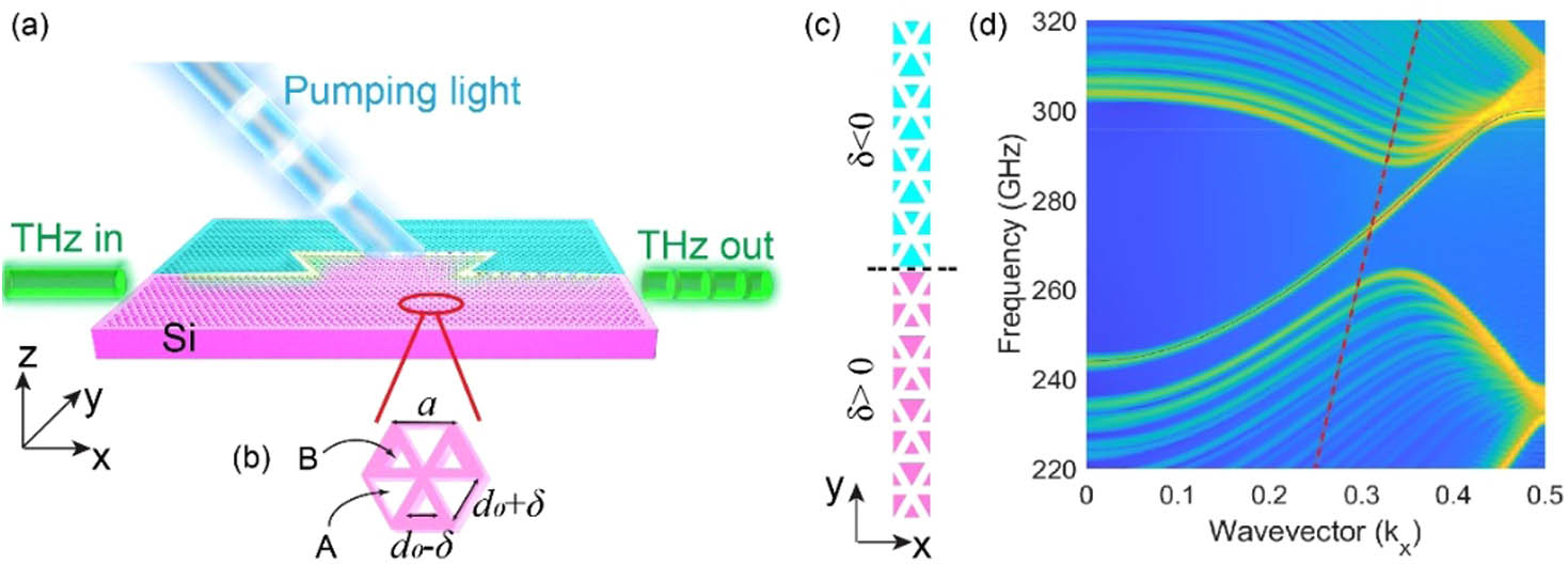
    Fig. 1. (a) THz topological photonic waveguide switch based on valley kink state. (b) Unit cell of the valley photonic crystal containing two types of triangular holes A and B with different sizes of a nonzero δ. The lattice constant is a. (c) Structure of the topological domain wall that supports the valley kink state. The black dashed line represents the interface between the two domains. (d) Band diagram of the valley kink state. The red dashed line represents the light line of the air cladding.
    (a) Optical image of the fabricated straight and bent VPC waveguide. (b) Optical microscopy image of the domain wall with opposite δ on each side. The black dashed line represents the interface between the two domains. The edge lengths were measured for triangular holes A and B labeled by red dashed lines. (c) Photo of the experimental setup for measuring the transmission spectra. The tapered structure was inserted into the WR-3 waveguide. (d) Simulated transmission spectra of the straight and bent VPC waveguide. (e) Measured transmission spectra of the straight and bent VPC waveguide. The gray area marks the bandgap region.
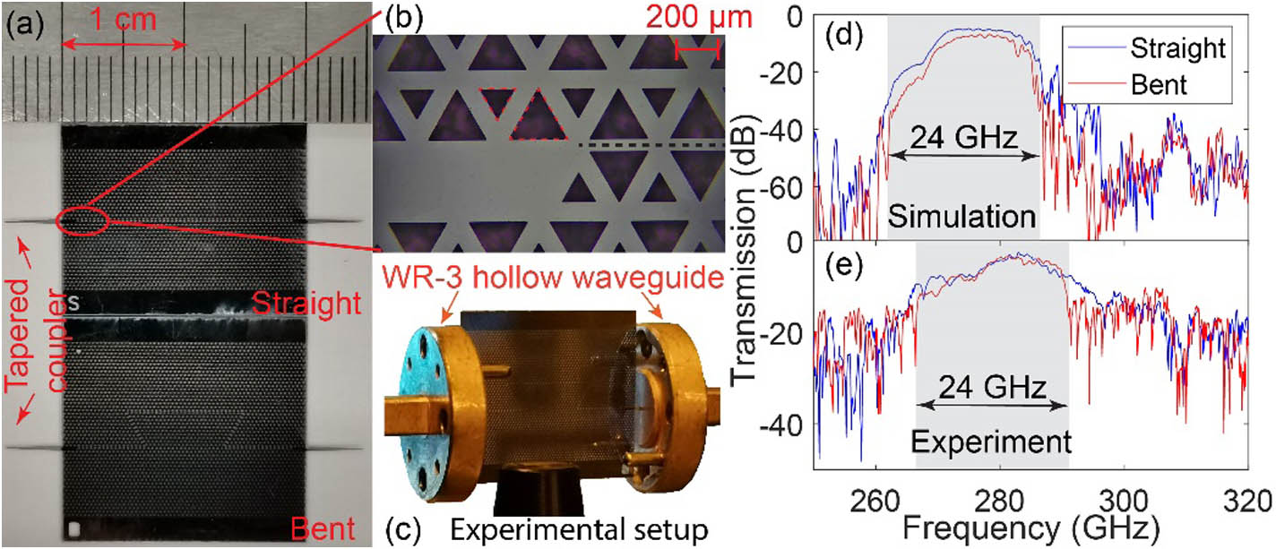
    Fig. 2. (a) Optical image of the fabricated straight and bent VPC waveguide. (b) Optical microscopy image of the domain wall with opposite δ on each side. The black dashed line represents the interface between the two domains. The edge lengths were measured for triangular holes A and B labeled by red dashed lines. (c) Photo of the experimental setup for measuring the transmission spectra. The tapered structure was inserted into the WR-3 waveguide. (d) Simulated transmission spectra of the straight and bent VPC waveguide. (e) Measured transmission spectra of the straight and bent VPC waveguide. The gray area marks the bandgap region.
    (a) Transmission spectra of the straight VPC for different S parameters. (b) Transmission spectra of the bent VPC for different S parameters. (c) Transmission spectra of the bent VPC with pumping light at 240 mW/mm2.
    Fig. 3. (a) Transmission spectra of the straight VPC for different S parameters. (b) Transmission spectra of the bent VPC for different S parameters. (c) Transmission spectra of the bent VPC with pumping light at 240  mW/mm2.
    (a) Photo of the experimental setup of the VPC waveguide switch. The pumping light is a fiber-coupled laser at 447 nm. The blue dashed double-head arrow indicates that the pumping light can be adjusted vertically. (b) The light spot was scanned from position 1 to position 5 to locate the best pumping position to the VPC waveguide. (c) Transmission spectra of various pumping positions at the same pumping intensity of 30 mW/mm2. (d) Transmission spectra with different pumping intensity (indicated on respective curves) at position 3.
    Fig. 4. (a) Photo of the experimental setup of the VPC waveguide switch. The pumping light is a fiber-coupled laser at 447 nm. The blue dashed double-head arrow indicates that the pumping light can be adjusted vertically. (b) The light spot was scanned from position 1 to position 5 to locate the best pumping position to the VPC waveguide. (c) Transmission spectra of various pumping positions at the same pumping intensity of 30  mW/mm2. (d) Transmission spectra with different pumping intensity (indicated on respective curves) at position 3.
    Schematic of an interchip communication system based on VPC waveguides. The pumping light can switch off the undesired channel to eliminate the interference. The black dashed line represents the undesired data transmission from Chip 1 to Chip 4, which interferes with the communication between Chip 5 and Chip 4 (marked by the solid green arrow).
    Fig. 5. Schematic of an interchip communication system based on VPC waveguides. The pumping light can switch off the undesired channel to eliminate the interference. The black dashed line represents the undesired data transmission from Chip 1 to Chip 4, which interferes with the communication between Chip 5 and Chip 4 (marked by the solid green arrow).
    (a) Schematic of photoexcited free-carrier lifetime measurement. The THz signal transmitted through the VPC device and was attenuated by the photoexcited carriers, which were generated by a modulated pumping beam shone at an oblique angle. (b) Experimental setup for carrier lifetime measurement.
    Fig. 6. (a) Schematic of photoexcited free-carrier lifetime measurement. The THz signal transmitted through the VPC device and was attenuated by the photoexcited carriers, which were generated by a modulated pumping beam shone at an oblique angle. (b) Experimental setup for carrier lifetime measurement.
    Modulation depth as a function of modulation frequency, showing the 3 dB modulation bandwidth of ∼60 kHz. The blue stars represent the experimental data, and the red line is a linear fit.
    Fig. 7. Modulation depth as a function of modulation frequency, showing the 3 dB modulation bandwidth of 60  kHz. The blue stars represent the experimental data, and the red line is a linear fit.
    Xudong Liu, Jialiang Huang, Hao Chen, Zhengfang Qian, Jingwen Ma, Xiankai Sun, Shuting Fan, Yiwen Sun. Terahertz topological photonic waveguide switch for on-chip communication[J]. Photonics Research, 2022, 10(4): 1090
    Download Citation