• Photonics Research
  • Vol. 10, Issue 4, 1090 (2022)
Xudong Liu1, Jialiang Huang1, Hao Chen1, Zhengfang Qian2, Jingwen Ma3, Xiankai Sun3, Shuting Fan2、4、*, and Yiwen Sun1、5、*
Author Affiliations
  • 1Department of Biomedical Engineering, School of Medicine, Shenzhen University, Shenzhen 518060, China
  • 2Key Laboratory of Optoelectronic Devices and Systems of Ministry of Education and Guangdong Province, College of Physics and Optoelectronics Engineering, Shenzhen University, Shenzhen 518060, China
  • 3Department of Electronic Engineering, The Chinese University of Hong Kong, Hong Kong, China
  • 4e-mail: shutingfan@szu.edu.cn
  • 5e-mail: ywsun@szu.edu.cn
  • show less
    DOI: 10.1364/PRJ.451344 Cite this Article Set citation alerts
    Xudong Liu, Jialiang Huang, Hao Chen, Zhengfang Qian, Jingwen Ma, Xiankai Sun, Shuting Fan, Yiwen Sun. Terahertz topological photonic waveguide switch for on-chip communication[J]. Photonics Research, 2022, 10(4): 1090 Copy Citation Text show less

    Abstract

    Terahertz (THz) topological photonic structures are promising for last-centimeter communication in intra/interchip communication systems because they support bit-error-free THz signal transmission with topological robustness. Active and dynamically tunable THz topological photonic components have not yet been experimentally realized. Here, we experimentally demonstrate a THz topological switch (270–290 GHz) based on a valley Hall photonic crystal structured high-resistivity silicon substrate, in which the THz waves can be dynamically turned on/off by an external 447 nm continuous-wave laser. Our device exhibited an on/off ratio of 19 dB under a pumping light intensity of 240 mW/mm2. The 3 dB switching bandwidth was 60 kHz.

    1. INTRODUCTION

    Terahertz (THz) waves are electromagnetic waves with frequencies between those of microwave and mid-infrared. This frequency region was previously called the “THz gap” [1] because of the difficulty in THz signal generation and detection. The rapid development of THz radiation sources and detectors [24] in recent decades has gradually closed the “THz gap” and demonstrated great potential in many areas, such as high-speed data transmission in ultrahigh-definition television systems [5,6]. Newly emerged applications, such as artificial intelligence and machine learning, also demand high-speed data transmission among advanced processing units, such as CPU, GPU, and TPU, in inter/intrachip systems [7,8]. The mismatch between heavy data computation and transmission among advanced processing units has created a new gap, the “interconnect gap” [8]. Advances in the THz region may help bridge the newly emerged “interconnect gap.” For example, a THz on-chip photonic waveguide based on a valley Hall photonic crystal (VPC) structure has been reported recently, which supports error-free transmission at a data transfer rate of up to 11  Gbits1 [9]. In the VPC channels, the valley kink states travel only along the paths with the same valley, which grants these states immunity to backscattering from sharp bends. Recently, photonic topological edge states have shown robust edge transport with strongly suppressed backscattering caused by disorders and sharp bends [1016], which is inspired by the concept of topological insulators in condensed-matter physics [17]. The conventional theory of backscattering suppression relies on the nonreciprocal effect [18,19], which is difficult to implement in the THz band, because many materials with the magneto-optical effect are not suitable for THz devices. Valley pseudospin is a new binary degree of freedom utilizing different corners of the hexagonal Brillouin zone of 2D Dirac materials [20,21]. The reduction of spatial-inversion symmetry can generate a nonvanishing valley-dependent Berry curvature and lead to quantum valley Hall effect without breaking the time-reversal symmetry [2224], which provides a valley kink state at the domain wall between regions of different topological valley phases. This additional strategy of topologically robust transport has been implemented in electronics [25], acoustics [26], and photonics [11]. The valley kink states are applied in routing, sorting, and splitting electromagnetic waves [27], which are useful for THz interconnects in an inter/intrachip system.

    To develop a fully integrated THz topological inter/intrachip communication system, it is necessary to integrate various functionalities such as waveguides, switches, and modulators on the same topological photonic crystal platform. However, most existing VPCs in the THz regime are limited to passive and static configurations, where the behavior of THz signals cannot be tuned dynamically at will. Experimental implementation of tunable topological VPC structures is, thus, a crucial step toward fully integrated topological THz communication systems. Here, we demonstrate a simple and low-cost method for dynamically tunable THz topological waveguides, based on which we realized effective on/off switching of THz waves. A VPC structured THz waveguide based on high-resistivity silicon with four 60° sharp corners operating at 270  GHz was fabricated. The nontrivial topology of the crystal ensures backscattering-free light propagation around the path with sharp turns and allows the structure to be immune to defects and imperfections. Photoexcited free carriers are initiated by a pumping beam, which produces a conductive layer on the silicon surface, resulting in absorption of the THz signal. Notably, our experiments are different from a previous one in the near-infrared regime [28] that was mainly based on tuning the refractive index of silicon with a femtosecond laser. The femtosecond laser is an expensive and bulky pulsed light source, which cannot continuously tune the valley photonic crystal structure. The VPC structure in Ref. [9] is a passive THz waveguide, which cannot be tuned actively. In our experiment, by exploiting a continuous-wave laser at λ=447  nm with a power density of 240  mW/mm2, an on/off ratio of 19 dB was achieved over a bandwidth of 20 GHz; the 3 dB switching bandwidth was as high as 60 kHz. Our results have demonstrated a low-cost and efficient approach to control the data transmission path in an inter/intrachip communication system.

    2. THEORY AND SIMULATION

    We designed photonic crystal structures on a high-resistivity silicon substrate, as shown in Fig. 1(a). The photonic crystal adopts a honeycomb lattice with a lattice constant a=340  μm. Each unit cell contains two triangular air holes A and B with side lengths of d0+δ and d0δ, respectively [Fig. 1(b)]. When these two triangular holes have the same size (δ=0), the photonic crystal has C6 point symmetry. Setting different dimensions of the triangles A and B with a nonvanishing δ breaks the spatial-inversion symmetry and reduces the point symmetry of the photonic crystal from C6 to C3. Here, the device pattern contains two different photonic crystal structures with opposite signs of δ, which are indicated by the cyan and red regions in Fig. 1(a). The use of the existing valley kink states to design topological integrated photonic devices at the interface between these two regions can be found in previous publications [9,27,28]. Here, the target operating frequency of our topological photonic device is 270 GHz, which is located in the frequency range of our vector network analyzer (VNA; 220–325 GHz). A 3D finite-difference time-domain method (Lumerical, FDTD solutions) was used for simulation. The zigzag-type boundary was selected [Fig. 1(c)], which theoretically conserves the valley pseudospin [9,27,28]. The photonic crystals on both sides of the domain wall possess the same parameters (d0=193  μm and |δ|=52  μm) with δ being positive (negative) in the red (cyan) region. Each unit cell comprises an equilateral triangular hole with a side length of d0+δ and an inverted equilateral triangular hole with a side length of d0δ. Figure 1(d) shows the simulated band diagram of the valley kink state, which matches our expected frequency and exhibits a topological behavior. Here, we focus on transverse-electric modes, where the electric fields oscillate in the plane. The modes propagating in the xy plane are confined in the z direction owing to total internal reflection.

    (a) THz topological photonic waveguide switch based on valley kink state. (b) Unit cell of the valley photonic crystal containing two types of triangular holes A and B with different sizes of a nonzero δ. The lattice constant is a. (c) Structure of the topological domain wall that supports the valley kink state. The black dashed line represents the interface between the two domains. (d) Band diagram of the valley kink state. The red dashed line represents the light line of the air cladding.

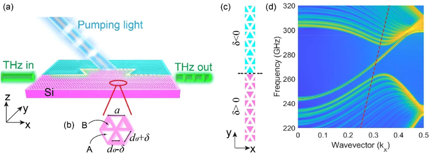
    Figure 1.(a) THz topological photonic waveguide switch based on valley kink state. (b) Unit cell of the valley photonic crystal containing two types of triangular holes A and B with different sizes of a nonzero δ. The lattice constant is a. (c) Structure of the topological domain wall that supports the valley kink state. The black dashed line represents the interface between the two domains. (d) Band diagram of the valley kink state. The red dashed line represents the light line of the air cladding.

    3. MATERIALS AND METHODS

    One of the most intriguing properties of topological valley kink states is that they are backscattering-free against sharp corners and preserve the valley pseudospin. To demonstrate this property, we employed photolithography and deep reactive-ion etching to fabricate a straight and a highly bent (trapezoidal) domain wall on a high-resistivity (>6  cm) silicon (relative permittivity 11.7) wafer with a thickness of h=170  μm, as shown in Figs. 2(a) and 2(b). Carefully designed terminals including a 5-mm-long tapered waveguide and a line-defect photonic crystal waveguide were fabricated to enable the efficient coupling of THz light to the valley kink states. At each turn, the momentum of the guided photons rotates by 2π/3, and the intervalley scattering is suppressed, resulting in backscattering-free light propagation.

    (a) Optical image of the fabricated straight and bent VPC waveguide. (b) Optical microscopy image of the domain wall with opposite δ on each side. The black dashed line represents the interface between the two domains. The edge lengths were measured for triangular holes A and B labeled by red dashed lines. (c) Photo of the experimental setup for measuring the transmission spectra. The tapered structure was inserted into the WR-3 waveguide. (d) Simulated transmission spectra of the straight and bent VPC waveguide. (e) Measured transmission spectra of the straight and bent VPC waveguide. The gray area marks the bandgap region.

    Figure 2.(a) Optical image of the fabricated straight and bent VPC waveguide. (b) Optical microscopy image of the domain wall with opposite δ on each side. The black dashed line represents the interface between the two domains. The edge lengths were measured for triangular holes A and B labeled by red dashed lines. (c) Photo of the experimental setup for measuring the transmission spectra. The tapered structure was inserted into the WR-3 waveguide. (d) Simulated transmission spectra of the straight and bent VPC waveguide. (e) Measured transmission spectra of the straight and bent VPC waveguide. The gray area marks the bandgap region.

    The pumping light (λ=447  nm) in the experiment can photoexcite free carriers in the high-resistivity silicon substrate. The photoexcited free carriers attenuate the transmitted signal beam with photon energies below the bandgap [29], such as THz radiation [2933]. The attenuation induced by the photoexcited free carriers can be described with the Drude model [34]. In the total internal reflection geometry, the modulation efficiency is much higher than that in the transmission geometry [30]. In our topological waveguide structure, by applying a pumping beam to photoexcite free carriers on the surface along the THz path, the transmitted THz signal can also be modulated effectively.

    Figure 2(b) shows the optical microscopy image of the lattice, which includes a “kink”-type domain wall between two VPCs with opposite δ values. A line-defect structure, also shown in Fig. 2(b), is used for coupling lights in a silicon strip waveguide with valley kink states. In the fabricated device, triangular hole A [highlighted with a large red dashed triangle in Fig. 2(b)] has a side length of 240 μm (245 μm in design), and triangular hole B [highlighted with a small red dashed triangle in Fig. 2(b)] has a side length of 159 μm (141 μm in design). VPCs that have intrinsically a weak topological phase are protected by certain crystalline symmetry, so they cannot survive from very strong random disorders that break the conservation of valley pseudospin. The size of the fabricated triangular holes has a <10% random disorder compared with designed parameters. We measured the transmission spectra of the devices with straight and bent domain walls using a well-calibrated VNA (AV3672E, 10 MHz–67 GHz) with two frequency extenders (AV3649A, 220–325 GHz). The transmission was normalized according to the calibration results of the VNA. When the two WR-3 waveguides are calibrated in the through standards, two WR-3 waveguides without samples are directly connected to measure the output power. In this condition, the transmission was treated as unity (0 dB). The terminals are carefully designed for efficient characterization of the valley kink states. Specifically, a tapered waveguide was fabricated and inserted into the WR-3 hollow waveguide to reduce the impedance mismatching and enhance light coupling efficiency into silicon strip waveguides [27]. Then a line-defect photonic crystal waveguide was used to achieve efficient excitation of the valley kink states. In our experiments, the relative positions between WR-3 waveguide and the tapered waveguide were carefully adjusted by micro-positioner to optimize the transmission spectra in the VNA. Figures 2(d) and 2(e) show the simulated and experimentally measured transmission spectra, respectively. In both the simulated and measured results, the transmission within the bulk band (from 270 to 285 GHz) with a bent and a straight domain walls had similar values. This confirms the theoretical prediction that the valley kink state is topologically robust against sharp bends in the bandgap frequency range. The measured results in our experiments indicate that the topological states still show certain robustness against the disorders in the fabrication process. The transmission is less than unity in the simulation because the light source is placed in the taper, which introduces some coupling loss. The loss in the experiment in the bandgap is around 4  dB, which is mainly the coupling loss between the WR-3 waveguide and tapered coupler. The relative frequency shift between the experimental and numerical transmission spectra can be attributed to the fact that the size of the fabricated triangular holes is slightly different from the designed values. The topological bandgap region is marked in gray in Figs. 2(d) and 2(e), where the topological theory guarantees the nearly same transmission spectra of the straight and bent waveguides. It should be noted that, at some frequencies outside this window, the straight waveguide can still exhibit relatively high transmission, but the light propagations at these frequencies are not topologically protected. Consequently, sharply bent waveguides exhibit much lower transmission at these frequencies.

    The transmission spectra (S11) and reflection spectra (S12) are presented in Figs. 3(a) and 3(b). By comparing the reflected signals in the devices with straight and bent domain walls, one can conclude that the sharp bends do not introduce additional backscattering. The relatively large backscattering signals in the measured results mainly originate from the terminals of the valley kink states. The backreflection around 285 GHz in Fig. 3(b) mainly occurs at (1) the interface between WR-3 hollow waveguide and (2) the interface between the line-defect photonic crystal waveguide and the valley kink states. It should be noted that such backscattering is not due to the sharp turns of the valley kink states because sharp turns do not introduce large intervalley scatterings. This can be confirmed by the experimental results in Fig. 3(c), which shows the measured reflection spectrum of S11 and S22 when the topological channels have been turned off by a strong visible light. One can clearly find that (1) S11 and S22 have different spectra because of the different relative positions between the WR-3 hollow waveguide and the tapered structures at the left and right terminals and (2) the energy levels of S11 and S22 remain almost unchanged even when the topological channels are turned off [see S12 in Fig. 3(c)]. The experimental results confirm that the measured backscattering mainly occurs outside the topological channels, which are also consistent with previous experiments using near-field mapping [35]. This can be confirmed by the fact that the Fabry–Perot-like interference in S11 can be greatly repressed when the valley kink states are turned off by the visible light, as shown in Fig. 3(c). The propagation loss of the VPC waveguide is low because (1) high-resistivity silicon shows low absorption in the THz regime, which was also reported in Ref. [9], and (2) the valley kink states lie below the light line and, thus, theoretically have zero radiation loss into the free space [36]. For these reasons, we expect that the propagation loss of the VPC waveguide mainly comes from imperfect fabrication processes, which is quite small and cannot be accurately quantified from our current experimental results.

    (a) Transmission spectra of the straight VPC for different S parameters. (b) Transmission spectra of the bent VPC for different S parameters. (c) Transmission spectra of the bent VPC with pumping light at 240 mW/mm2.

    Figure 3.(a) Transmission spectra of the straight VPC for different S parameters. (b) Transmission spectra of the bent VPC for different S parameters. (c) Transmission spectra of the bent VPC with pumping light at 240  mW/mm2.

    4. RESULTS AND DISCUSSION

    A fiber-coupled continuous-wave laser (λ=447  nm) was used to photoexcite the device with bent domain walls, as shown in Fig. 4(a). The pumping laser featured a TEM00 transverse mode, and the circular light spot had a radius of 1.8  mm and a size of 10  mm2. To properly align the light spot with the topological waveguide (THz propagation path), the laser (power fixed at 300 mW) was linearly scanned over 4 mm with a step of 500 μm, as shown in Fig. 4(b). The relationship between the pumping position and transmission spectrum at five selected positions is plotted in Fig. 4(c). The attenuation of the THz wave is from the absorption of photoexcited free carriers. When the pumping light spot fully covers the VPC waveguide, the transmitted THz radiation interacts with the most free carriers. When the pumping light spot is moved away from the VPC waveguide, only a small number of photoexcited carriers can drift to the waveguide; thus, the attenuation of the THz radiation is slight. The transmission spectra are plotted only in the range of 270–290 GHz to show the transmission difference more clearly. The lowest transmission is achieved at position 3, which indicates the best alignment between the pumping light spot and topological waveguide. Figure 4(c) also demonstrates that, when the pumping light was shifted 2 mm away from the topological waveguide, the attenuation effect was close to that without the pumping beam. This suggests that the drift distance of the photoexcited free carriers in the silicon substrate was less than 2 mm. Next, the power intensity of the pumping laser was tuned from 0 to 240  mW/mm2. In Fig. 4(d), the transmission decreases with increasing pumping intensity and reaches a minimum of 23  dB when the pumping intensity is 240  mW/mm2. By comparing the transmission of 4  dB without the pumping light, we determined the on/off ratio to be 19 dB. The pumping intensity did not increase further because the transmission was already on the noise floor.

    (a) Photo of the experimental setup of the VPC waveguide switch. The pumping light is a fiber-coupled laser at 447 nm. The blue dashed double-head arrow indicates that the pumping light can be adjusted vertically. (b) The light spot was scanned from position 1 to position 5 to locate the best pumping position to the VPC waveguide. (c) Transmission spectra of various pumping positions at the same pumping intensity of 30 mW/mm2. (d) Transmission spectra with different pumping intensity (indicated on respective curves) at position 3.

    Figure 4.(a) Photo of the experimental setup of the VPC waveguide switch. The pumping light is a fiber-coupled laser at 447 nm. The blue dashed double-head arrow indicates that the pumping light can be adjusted vertically. (b) The light spot was scanned from position 1 to position 5 to locate the best pumping position to the VPC waveguide. (c) Transmission spectra of various pumping positions at the same pumping intensity of 30  mW/mm2. (d) Transmission spectra with different pumping intensity (indicated on respective curves) at position 3.

    Figure 5 illustrates the application scenario of our VPC waveguide optical switch in a multiprocessor on-chip communication system. To achieve high-speed communication among different processors, we should make full use of the 20 GHz bandwidth in our VPC design. For example, when Chip 1 communicates with Chip 2, the desired data transmission path is marked by the solid black arrow in Fig. 5. However, the signal would also be transmitted to Chip 4 by following the dashed black path, which interferes with the communication frequency channel between Chips 5 and 4 (marked by the solid green arrow), leading to the 20 GHz bandwidth resource not being fully used. Techniques such as wavelength-division multiplexing can be used to overcome channel interference, but they lower the data transmission speed and complicate the system. Instead, by focusing an external pumping beam on the topological waveguide (as marked by the round spot in Fig. 5), interference with the communication channel to Chip 4 can be eliminated. In practical applications, light from an array of semiconductor laser diodes can be allocated to different topological waveguide channels, which form a programmable information network among the processors in an interchip communication system. Therefore, our method provides a low-cost solution to the channel interference issue while maintaining the communication rate in the THz interconnect system.

    Schematic of an interchip communication system based on VPC waveguides. The pumping light can switch off the undesired channel to eliminate the interference. The black dashed line represents the undesired data transmission from Chip 1 to Chip 4, which interferes with the communication between Chip 5 and Chip 4 (marked by the solid green arrow).

    Figure 5.Schematic of an interchip communication system based on VPC waveguides. The pumping light can switch off the undesired channel to eliminate the interference. The black dashed line represents the undesired data transmission from Chip 1 to Chip 4, which interferes with the communication between Chip 5 and Chip 4 (marked by the solid green arrow).

    Theoretically, the switching speed of our design is limited by the lifetime of the photoexcited free carriers in the silicon substrate. We could not measure the on/off switching speed directly from 270 to 290 GHz owing to the limited functionalities of our VNA. We did not perform time-resolved THz spectroscopy because the lifetime of free carriers in high-resistivity silicon is usually beyond its measurable range. The modulation effect from the free carriers is broadband to the THz signal [30]. Thus, it is reasonable to use a continuous-wave THz source (100 GHz, from Terasense Group Inc.) to measure the photoexcited carrier lifetime. The THz source was normally incident to the VPC device surface, and the pumping light was shone on the device at an oblique angle [Fig. 6(a)]. The pumping light was triggered by a transistor-transistor-logic (TTL) signal at various frequencies ranging from 0 to 110 kHz. The details of the experimental setup are provided in Fig. 6(b). Using this method, we could calculate the lifetime of the free carriers and estimate the switching speed of the VPC waveguide. The normalized modulation depth was calculated based on the modulation results at a triggered frequency of zero. The 3 dB modulation bandwidth in the transmission configuration was 60  kHz as shown in Fig. 7. The modulation performance from the free carriers in the total internal reflection geometry is normally better than that in the transmission geometry [30]. The modes propagating in the VPC waveguide are confined in the z direction owing to total internal reflection; it is reasonable to estimate the modulation speed of the VPC waveguide is approximately or larger than 60 kHz.

    (a) Schematic of photoexcited free-carrier lifetime measurement. The THz signal transmitted through the VPC device and was attenuated by the photoexcited carriers, which were generated by a modulated pumping beam shone at an oblique angle. (b) Experimental setup for carrier lifetime measurement.

    Figure 6.(a) Schematic of photoexcited free-carrier lifetime measurement. The THz signal transmitted through the VPC device and was attenuated by the photoexcited carriers, which were generated by a modulated pumping beam shone at an oblique angle. (b) Experimental setup for carrier lifetime measurement.

    Modulation depth as a function of modulation frequency, showing the 3 dB modulation bandwidth of ∼60 kHz. The blue stars represent the experimental data, and the red line is a linear fit.

    Figure 7.Modulation depth as a function of modulation frequency, showing the 3 dB modulation bandwidth of 60  kHz. The blue stars represent the experimental data, and the red line is a linear fit.

    5. CONCLUSION

    We proposed and experimentally demonstrated an optical approach for effectively switching on/off the VPC waveguide. The bent VPC waveguide based on a high-resistivity silicon substrate shows immunity to backscattering at sharp bends and has an operating band from 270 to 290 GHz. THz-absorbing free carriers were generated by a 447 nm continuous-wave laser to effectively switch off the waveguide. With a pumping intensity of 240  mW/mm2, an on/off ratio of 19 dB was achieved over the entire operating band, and the 3 dB modulation bandwidth was measured to be 60  kHz. The optical switch can easily be integrated into the THz interconnect communication system to actively control the data transmission channels. The modulation speed was limited by the long carrier lifetime of high-resistivity silicon; it is expected that the switching speed can be further increased by using semiconductors with a shorter carrier lifetime in the future.

    References

    [1] C. Sirtori. Bridge for the terahertz gap. Nature, 417, 132-133(2002).

    [2] S. Dhillon, M. Vitiello, E. Linfield, A. Davies, M. C. Hoffmann, J. Booske, C. Paoloni, M. Gensch, P. Weightman, G. Williams. The 2017 terahertz science and technology roadmap. J. Phys. D, 50, 043001(2017).

    [3] D. M. Mittleman. Perspective: terahertz science and technology. J. Appl. Phys., 122, 230901(2017).

    [4] M. Tonouchi. Cutting-edge terahertz technology. Nat. Photonics, 1, 97-105(2007).

    [5] T. Kleine-Ostmann, T. Nagatsuma. A review on terahertz communications research. J. Infrared Millimeter Terahertz Waves, 32, 143-171(2011).

    [6] T. Nagatsuma, G. Ducournau, C. C. Renaud. Advances in terahertz communications accelerated by photonics. Nat. Photonics, 10, 371-379(2016).

    [7] J. W. Holloway, G. C. Dogiamis, R. Han. Innovations in terahertz interconnects: high-speed data transport over fully electrical terahertz waveguide links. IEEE Microw. Mag., 21, 35-50(2020).

    [8] Q. J. Gu. THz interconnect: the last centimeter communication. IEEE Commun. Mag., 53, 206-215(2015).

    [9] Y. Yang, Y. Yamagami, X. Yu, P. Pitchappa, J. Webber, B. Zhang, M. Fujita, T. Nagatsuma, R. Singh. Terahertz topological photonics for on-chip communication. Nat. Photonics, 14, 446-451(2020).

    [10] J. Dong, X. Chen, H. Zhu, Y. Wang, X. Zhang. Valley photonic crystals for control of spin and topology. Nat. Mater., 16, 298-302(2017).

    [11] J. Noh, S. Huang, K. P. Chen, M. C. Rechtsman. Observation of photonic topological valley Hall edge states. Phys. Rev. Lett., 120, 063902(2018).

    [12] M. I. Shalaev, W. Walasik, A. Tsukernik, Y. Xu, N. M. Litchinitser. Robust topologically protected transport in photonic crystals at telecommunication wavelengths. Nat. Nanotechnol., 14, 31-34(2019).

    [13] L. Lu, J. D. Joannopoulos, M. Soljačić. Topological photonics. Nat. Photonics, 8, 821-829(2014).

    [14] T. Ozawa, H. M. Price, A. Amo, N. Goldman, M. Hafezi, L. Lu, M. C. Rechtsman, D. Schuster, J. Simon, O. Zilberberg, I. Carusotto. Topological photonics. Rev. Mod. Phys., 91, 015006(2019).

    [15] X. Wu, Y. Meng, J. Tian, Y. Huang, H. Xiang, D. Han, W. Wen. Direct observation of valley-polarized topological edge states in designer surface plasmon crystals. Nat. Commun., 8, 1304(2017).

    [16] B.-Y. Xie, H.-F. Wang, X.-Y. Zhu, M.-H. Lu, Z. D. Wang, Y.-F. Chen. Photonics meets topology. Opt. Express, 26, 24531-24550(2018).

    [17] M. Z. Hasan, C. L. Kane. Colloquium: topological insulators. Rev. Mod. Phys., 82, 3045-3067(2010).

    [18] B. Bahari, A. Ndao, F. Vallini, A. E. Amili, Y. Fainman, B. Kanté. Nonreciprocal lasing in topological cavities of arbitrary geometries. Science, 358, 636-640(2017).

    [19] K. Fang, Z. Yu, S. Fan. Realizing effective magnetic field for photons by controlling the phase of dynamic modulation. Nat. Photonics, 6, 782-787(2012).

    [20] H. Zeng, J. Dai, W. Yao, D. Xiao, X. Cui. Valley polarization in MoS2 monolayers by optical pumping. Nat. Nanotechnol., 7, 490-493(2012).

    [21] J. R. Schaibley, H. Yu, G. Clark, P. Rivera, J. S. Ross, K. L. Seyler, W. Yao, X. Xu. Valleytronics in 2D materials. Nat. Rev. Mater., 1, 16055(2016).

    [22] M. Hafezi, E. A. Demler, M. D. Lukin, J. M. Taylor. Robust optical delay lines with topological protection. Nat. Phys., 7, 907-912(2011).

    [23] T. Ma, A. B. Khanikaev, S. H. Mousavi, G. Shvets. Guiding electromagnetic waves around sharp corners: topologically protected photonic transport in metawaveguides. Phys. Rev. Lett., 114, 127401(2015).

    [24] A. B. Khanikaev, S. H. Mousavi, W. K. Tse, M. Kargarian, A. H. MacDonald, G. Shvets. Photonic topological insulators. Nat. Mater., 12, 233-239(2013).

    [25] L. Ju, Z. Shi, N. Nair, Y. Lv, C. Jin, J. Velasco, C. Ojeda-Aristizabal, H. A. Bechtel, M. C. Martin, A. Zettl, J. Analytis, F. Wang. Topological valley transport at bilayer graphene domain walls. Nature, 520, 650-655(2015).

    [26] J. Lu, C. Qiu, L. Ye, X. Fan, M. Ke, F. Zhang, Z. Liu. Observation of topological valley transport of sound in sonic crystals. Nat. Phys., 13, 369-374(2017).

    [27] J. Ma, X. Xi, X. Sun. Topological photonic integrated circuits based on valley kink states. Laser Photon. Rev., 13, 1900087(2019).

    [28] M. I. Shalaev, W. Walasik, N. M. Litchinitser. Optically tunable topological photonic crystal. Optica, 6, 839-844(2019).

    [29] I. H. Libon, S. Baumgärtner, M. Hempel, N. E. Hecker, J. Feldmann, M. Koch, P. Dawson. An optically controllable terahertz filter. Appl. Phys. Lett., 76, 2821-2823(2000).

    [30] X. Liu, E. P. J. Parrott, B. S.-Y. Ung, E. Pickwell-MacPherson. Exploiting total internal reflection geometry for efficient optical modulation of terahertz light. APL Photon., 1, 076103(2016).

    [31] P. Weis, J. L. Garcia-Pomar, M. Höh, B. Reinhard, A. Brodyanski, M. Rahm. Spectrally wide-band terahertz wave modulator based on optically tuned graphene. ACS Nano, 6, 9118-9124(2012).

    [32] T. He, B. Zhang, G.-C. Wang, Y.-B. Hou, J.-L. Shen. High efficiency THz-wave modulators based on conjugated polymer-based organic films. J. Phys. D, 49, 075111(2016).

    [33] D. Shrekenhamer, C. M. Watts, W. J. Padilla. Terahertz single pixel imaging with an optically controlled dynamic spatial light modulator. Opt. Express, 21, 12507-12518(2013).

    [34] M. van Exter, D. Grischkowsky. Carrier dynamics of electrons and holes in moderately doped silicon. Phys. Rev. B, 41, 12140-12149(1990).

    [35] K.-Q. Lin. A roadmap for interlayer excitons. Light Sci. Appl., 10, 99(2021).

    [36] E. Sauer, J. P. Vasco, S. Hughes. Theory of intrinsic propagation losses in topological edge states of planar photonic crystals. Phys. Rev. Res., 2, 043109(2020).

    Xudong Liu, Jialiang Huang, Hao Chen, Zhengfang Qian, Jingwen Ma, Xiankai Sun, Shuting Fan, Yiwen Sun. Terahertz topological photonic waveguide switch for on-chip communication[J]. Photonics Research, 2022, 10(4): 1090
    Download Citation