• Journal of Semiconductors
  • Vol. 40, Issue 4, 042601 (2019)
Lei Tang1、2, Kwong-Hoi Tsui1、2, Siu-Fung Leung3, Qianpeng Zhang1、2, Matthew Kam1、2, Hsin-Ping Wang3, Jr-Hau He3, and Zhiyong Fan1、2
Author Affiliations
  • 1HKUST-Shenzhen Research Institute, Shenzhen 518057, China
  • 2Department of Electronic and Computer Engineering, Hong Kong University of Science and Technology (HKUST), Hong Kong, China
  • 3Computer, Electrical and Mathematical Sciences and Engineering, King Abdullah University of Science and Technology, Thuwai 23955-6900, Kingdom of Saudi Arabia
  • show less
    DOI: 10.1088/1674-4926/40/4/042601 Cite this Article
    Lei Tang, Kwong-Hoi Tsui, Siu-Fung Leung, Qianpeng Zhang, Matthew Kam, Hsin-Ping Wang, Jr-Hau He, Zhiyong Fan. Large-scale, adhesive-free and omnidirectional 3D nanocone anti-reflection films for high performance photovoltaics[J]. Journal of Semiconductors, 2019, 40(4): 042601 Copy Citation Text show less
    (Color online) Schematic diagram of fabrication process of i-cone mold and AR film, and SEM images of Au-coated mold and PDMS nanocone. (a) A 4-inch glass wafer with sputtered 5 μm pure aluminum on the surface underwent photolithography of 1 μm hexagonal array pattern. (b) The pattern wafer underwent dry etching to form 50 nm-depth nanoindentation. (c) The wafer underwent anodization to form i-nanocone arrays. (d) The replication and peeloff process of AR film. (e) SEM of Au-coated mold with 1 μm pitch and 1 μm depth. (f) SEM of nanocone with 1 μm pitch and 1 μm depth.
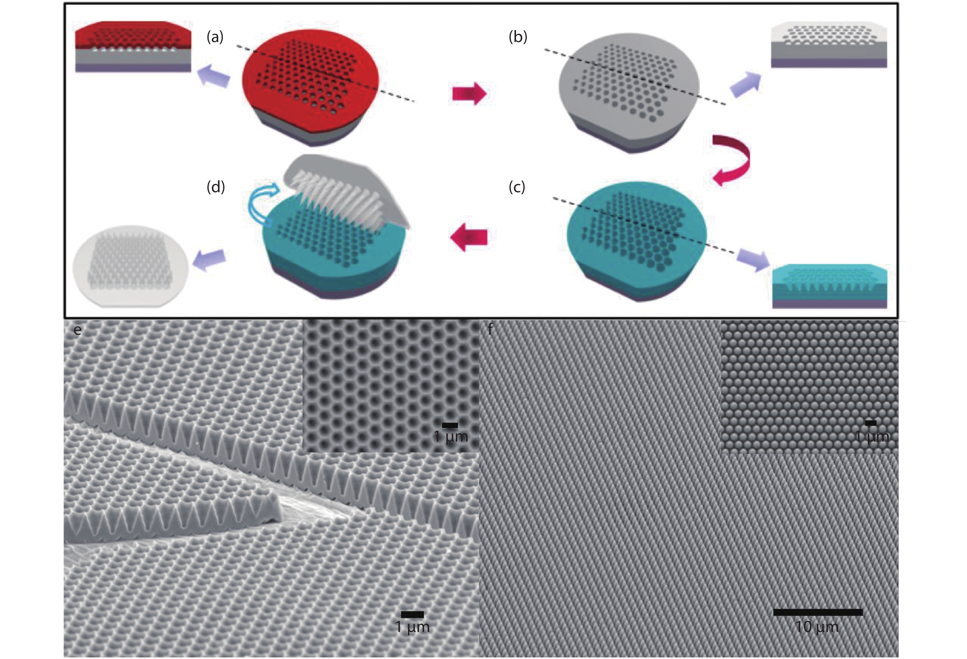
    Fig. 1. (Color online) Schematic diagram of fabrication process of i-cone mold and AR film, and SEM images of Au-coated mold and PDMS nanocone. (a) A 4-inch glass wafer with sputtered 5 μm pure aluminum on the surface underwent photolithography of 1 μm hexagonal array pattern. (b) The pattern wafer underwent dry etching to form 50 nm-depth nanoindentation. (c) The wafer underwent anodization to form i-nanocone arrays. (d) The replication and peeloff process of AR film. (e) SEM of Au-coated mold with 1 μm pitch and 1 μm depth. (f) SEM of nanocone with 1 μm pitch and 1 μm depth.
    (Color online) (a) The photograph of 4-inch Au-coated mold. (b) The photograph of flexible AR film attached on polycarbonate film. (c) Schematic diagram of the c-Si solar cell device with nanocone AR film attached on the top. (d) Real 8 cm by 8 cm AR film attached on c-Si device.
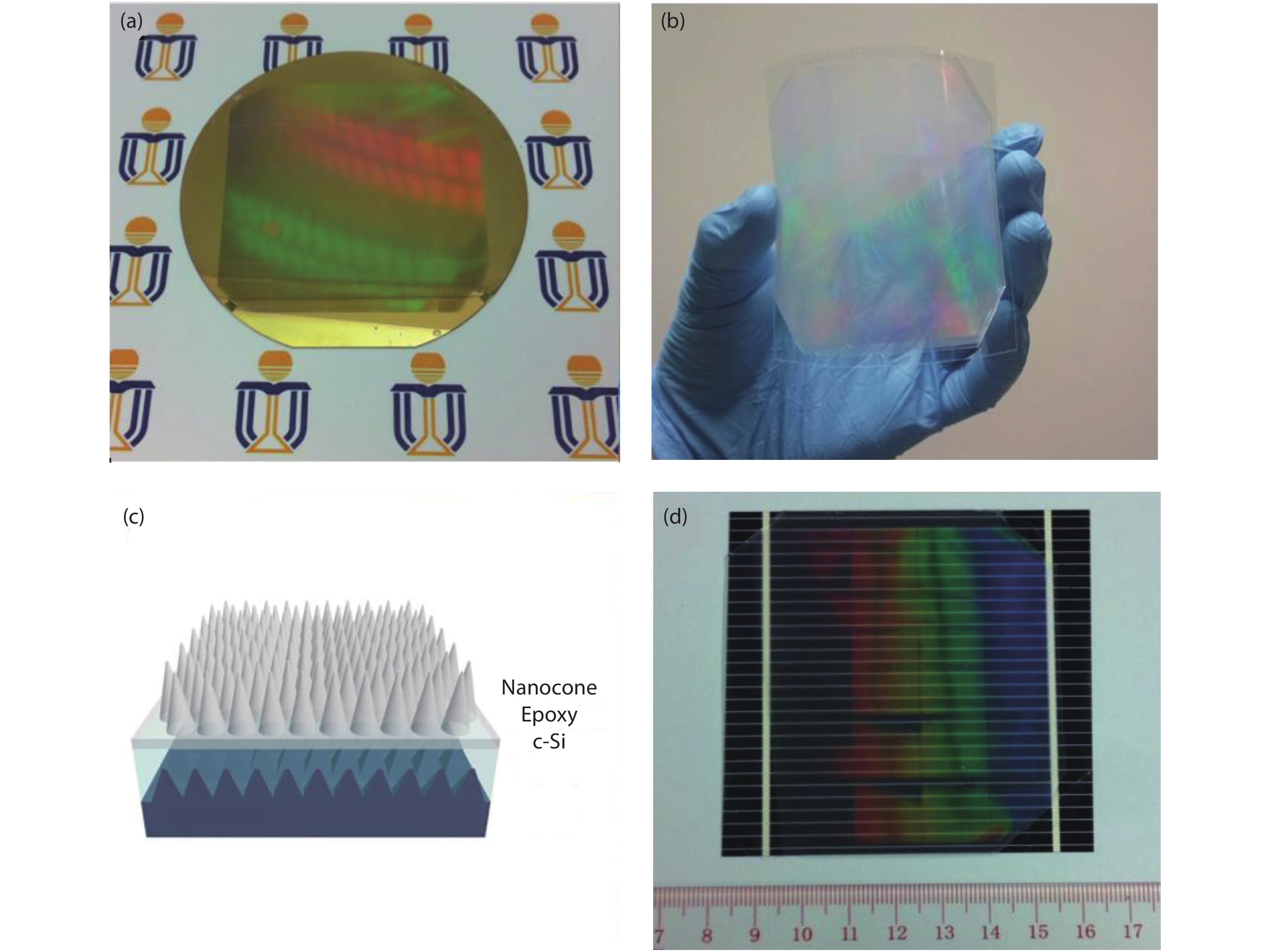
    Fig. 2. (Color online) (a) The photograph of 4-inch Au-coated mold. (b) The photograph of flexible AR film attached on polycarbonate film. (c) Schematic diagram of the c-Si solar cell device with nanocone AR film attached on the top. (d) Real 8 cm by 8 cm AR film attached on c-Si device.
    (Color online) (a) The reflectance spectra of c-Si solar cell device with and without epoxy layer and nanocone AR film in optical wavelength from 400 to 900 nm. (b) Simulations of reflectance spectra in optical wavelength from 400 to 900 nm of c-Si solar cell device with and without epoxy layer and nanocone AR film. (c) Simulated |E|2 distribution of electromagnetic wave at 650 nm wavelength for the bare c-Si device. (d) Simulated |E|2 distribution of electromagnetic wave at 650 nm wavelength for the epoxy-encapsulated c-Si device. (e) Simulated |E|2 distribution of electromagnetic wave at 650 nm wavelength for the AR film-attached c-Si device. (f) QE measurement of c-Si solar cell device with and without epoxy layer and nanocone AR film.
    Fig. 3. (Color online) (a) The reflectance spectra of c-Si solar cell device with and without epoxy layer and nanocone AR film in optical wavelength from 400 to 900 nm. (b) Simulations of reflectance spectra in optical wavelength from 400 to 900 nm of c-Si solar cell device with and without epoxy layer and nanocone AR film. (c) Simulated |E|2 distribution of electromagnetic wave at 650 nm wavelength for the bare c-Si device. (d) Simulated |E|2 distribution of electromagnetic wave at 650 nm wavelength for the epoxy-encapsulated c-Si device. (e) Simulated |E|2 distribution of electromagnetic wave at 650 nm wavelength for the AR film-attached c-Si device. (f) QE measurement of c-Si solar cell device with and without epoxy layer and nanocone AR film.
    (Color online) (a) Reflectance spectra of a c-Si solar cell device with and without epoxy layer and AR film obtained for the light incident angles tuning from 0° (normal incident) to 60° at 10° intervals. (b) Jsc of a c-Si device with and without epoxy layer and AR film obtained at different incident angles, together with the angular-dependent relative improvement of Jsc. (c) Power output of a c-Si device with and without epoxy layer and AR film against daytime. (d) Power output improvement of a c-Si device with and without epoxy layer and nanostructure AR film against daytime, with their daily energy output in the inset.
    Fig. 4. (Color online) (a) Reflectance spectra of a c-Si solar cell device with and without epoxy layer and AR film obtained for the light incident angles tuning from 0° (normal incident) to 60° at 10° intervals. (b) Jsc of a c-Si device with and without epoxy layer and AR film obtained at different incident angles, together with the angular-dependent relative improvement of Jsc. (c) Power output of a c-Si device with and without epoxy layer and AR film against daytime. (d) Power output improvement of a c-Si device with and without epoxy layer and nanostructure AR film against daytime, with their daily energy output in the inset.
    Lei Tang, Kwong-Hoi Tsui, Siu-Fung Leung, Qianpeng Zhang, Matthew Kam, Hsin-Ping Wang, Jr-Hau He, Zhiyong Fan. Large-scale, adhesive-free and omnidirectional 3D nanocone anti-reflection films for high performance photovoltaics[J]. Journal of Semiconductors, 2019, 40(4): 042601
    Download Citation