
Lei Tang, Kwong-Hoi Tsui, Siu-Fung Leung, Qianpeng Zhang, Matthew Kam, Hsin-Ping Wang, Jr-Hau He, Zhiyong Fan. Large-scale, adhesive-free and omnidirectional 3D nanocone anti-reflection films for high performance photovoltaics[J]. Journal of Semiconductors, 2019, 40(4): 042601
- Journal of Semiconductors
- Vol. 40, Issue 4, 042601 (2019)
Abstract
1. Introduction
Photovoltaic (PV) systems have been widely deployed as a major renewable energy resource in our daily life because they can directly convert solar energy into clean electricity without pollutions. Typically, solar panels are installed outdoors and exposed to all weather conditions, therefore they are normally packaged with protection layers[
2. Experimental
2.1. Fabrication of i-cone mold
A layer of 5 μm of pure aluminum was sputtered on 4-inches glass wafer using Varian 3180 Sputtering System (SPT-3180). The hexagonal-array nanoindentation with depth of 50 nm and pitch of 1μm was formed on Al surface through photolithography and dry etching process using ASML Stepper 5000 (PHT-S1) and AST Cirie 200 Etcher (DRY-Metal), respectively. Photoresist AZ7908 was used as the mask in the processes. Afterwards, the inverse-cone (i-cone) array was fabricated using multi-step anodization and wet etching on the Al/Glass wafer on an acidic solution with a proper direct-current (DC) voltages as mentioned in our previous works[
2.2. Fabrication of nanocone AR films
A premixed and degassed PDMS (Sylgard 184, Dow Corning 10 : 1 ratio with the curing agent) was directly poured on the Au-coated icone mold. It should be noted that multiple molds can be stitched together as shown in Supplementary Information (Fig. S2(a)) so that an industrial-scale mold can be formed. Afterwards, PDMS was cured at 120 °C for 5 min. Finally, the large-scale PDMS film can be directly peeled off from the mold.
2.3. Device characterization
SEM images were taken by a JEOL JSM-7100F SEM working at 10 kV. UV–Vis spectra of all devices were obtained using home-built ultraviolet/visible measurement setup. The QE measurement of c-Si solar cell devices were carried out by Oriel QE-PV-SI (Newport Corporation). All theJ–V curves were obtained using solar simulator (Newport Corporation. 91150V) under 1 Sun illumination
3. Results and discussion
In this work, we report a new technique to fabricate a large-scale, adhesive-free and omnidirectional 3-D nanocone anti-reflection films for high performance photovoltaics. The flexible AR films were fabricated by directly replicating inverse-nanocone (i-cone) arrays on the surface of the mold using polydimethylsiloxane (PDMS). It is worth noting that the mold can be reused multiple times without leaving any residue. Moreover, a scalable mold can be achieved by the stitching of molds to achieve different sizes for commercial solar panels. Therefore, the developed approach makes the manufacturing process cost-effective. The effectiveness of the films has been evaluated using polycrystalline Si solar cells. Overall, the light reflectance measurements and finite-difference-time-domain (FDTD) simulations have shown that the 3D nanocone arrays can significantly reduce the surface reflectance of the encapsulation layer and more pronounced improvements have been observed at oblique light incident angles, which are meaningful for practical case. As a result, the nanocone AR films have boosted the daily energy output of the solar cell devices from 0.774 to 0.844 kWh/m2, which is close to a 10% enhancement over the device without the AR film.
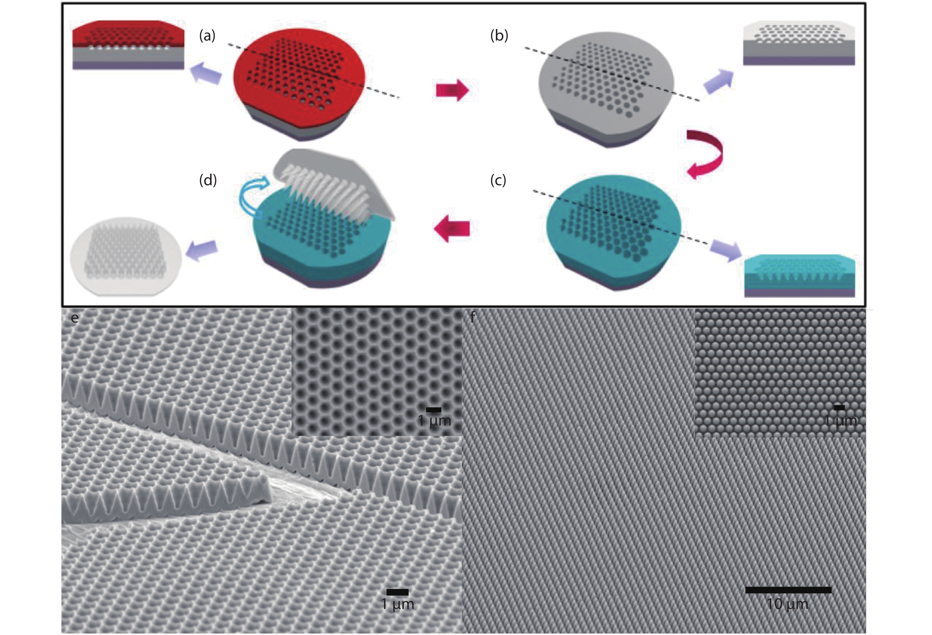
The large-scale AR films were fabricated by directly replicating inverse-nanocone (i-cone) arrays on a 4-inch wafer using polydimethylsiloxane (PDMS) which is a proper material for AR films because of its high UV resistance, flexibility and optical transparency[
![]()
Figure 1.(Color online) Schematic diagram of fabrication process of i-cone mold and AR film, and SEM images of Au-coated mold and PDMS nanocone. (a) A 4-inch glass wafer with sputtered 5
There are several distinct features in our fabrication process and films making it superior to the existing anti-reflection technologies. Fig. 2(a) shows a 4-inch i-cone mold coated with 50 nm gold. The light diffraction effect on the surface of the mold indicates the excellent regularity of the nanostructures on the top. The size of the mold can be increased from 4 inches to 12 inches or even larger by using a larger glass wafer. Moreover, it is noteworthy that molds can also be scaled up by directly stitching them together as shown in Fig. S1(a) in supporting Information. Therefore, as shown in Fig. S1(b), tailored size of films can be made for different sizes of commercial solar panels in the market.
![]()
Figure 2.(Color online) (a) The photograph of 4-inch Au-coated mold. (b) The photograph of flexible AR film attached on polycarbonate film. (c) Schematic diagram of the c-Si solar cell device with nanocone AR film attached on the top. (d) Real 8 cm by 8 cm AR film attached on c-Si device.
Fig. 2(b) shows the AR film attached to a 180 μm-thick polycarbonate film. Ease of attachment and detachment is one of the appealing features of the nanocone AR film. Traditional AR techniques such as λ/4 coating and texturization are applied to the surface of solar cells. However, these AR layers are irreplaceable when damaged. Worse still, the damaged layers become a light blocking layer which sacrifices the efficiency of solar cell devices[
Optical reflectance spectra with wavelength from 400 to 900 nm are shown in Fig. 3(a) in order to quantitatively study the antireflection performance of the AR films. c-Si devices with and without attaching the AR film were placed at the normal direction to the light beam inside an integrated sphere of a home-built ultraviolet/visible measurement setup. The optical reflectance spectrum of an epoxy-encapsulated sample was also measured to evaluate the effect of encapsulated materials on bare c-Si solar cell devices and verify the enhancement effect of AR films on commercial packaged solar cell devices. In the entire visible light region, the AR film-attached c-Si device showed apparently lower reflectance compared to the bare and epoxy-encapsulated c-Si devices. The integrated reflectance of the AR film-attached c-Si device was suppressed to 4.62% while that of the bare and epoxyencapsulated c-Si device were 5.62% and 6.24% respectively. In other words, the AR film reduced light reflectance by 17.7% and 26.0% when respectively compared to the bare and epoxyencapsulated c-Si device, respectively. The reduction of reflectance is mainly due to the tapered nanocone shape, which provides a gradual change of effective refractive index[
![]()
Figure 3.(Color online) (a) The reflectance spectra of c-Si solar cell device with and without epoxy layer and nanocone AR film in optical wavelength from 400 to 900 nm. (b) Simulations of reflectance spectra in optical wavelength from 400 to 900 nm of c-Si solar cell device with and without epoxy layer and nanocone AR film. (c) Simulated |
To verify the reflectance spectra obtained from the experiments, optical simulation were performed using FDTD method with results shown in Fig. 3(b). In the FDTD simulation of reflectance spectra, the overall trend for those three devices is consistent with the result obtained from experiments. The AR film showed an excellent reduction in light reflection for the visible light region. On the contrary, both the bare Si and epoxy-encapsulated device showed higher reflection than with AR film. This means epoxy itself cannot reduce the light reflection and the nanostructure plays a key role for AR. In order to understand the AR mechanism in nanostructures, more specifically the nanocones, the cross-sectional electric field intensity (|E|2) distribution were studied and the results are shown in Figs. 3(c)–3(e). Noting that electromagnetic (EM) plane waves propagate downwards from z = 5.5 μm. A c-Si pyramid arrays was used to imitate the surface roughness of c-Si device. Epoxy thin film and nanocones were added to the devices in Figs. 3(d) and 3(e) respectively. The base of a c-Si pyramid, the top surface of epoxy and the top of the nanocone locate at z = −1.5, 2.5 and 4.5 μm respectively more importantly, the color above z = 5.5 μm manifests the intensity of the reflected wave. It can be seen that the existence of nanocone results in the weakest intensity of the reflected wave among these three models, which clearly demonstrates the AR effect of nanocones. The reason for the AR effect is that the nanocones, working as focusing lens, strongly couples the light into the device, as can be clearly seen in Fig. 3(e).
The main function of AR layer is to reduce the optical reflectance on solar cells so that more incoming photons can be utilized and, eventually, the device performance can be enhanced. Therefore, the external quantum efficiency (EQE) measurement was conducted for those three devices. From the result, the EQE curve of the AR film-attached c-Si device is obviously higher than others. It provides a direct evidence of the AR effect. Notably, the EQE at 650 nm reaches almost 95% which is extraordinarily high in c-Si devices. Regarding the EQE current density (QE Jsc), the QE Jsc of c-Si device after using the AR film was increased from 27.5 to 28.8 mA/cm2, which indicated around a 4% enhancement. Research has shown that it is challenging for high-efficiency solar cells to have a marginal improvement. In the industry, enhancing the device performance may involve re-designing device structures which may lead to a high capital investment. Introducing an additional AR film on the top of the device can make industrial process cheaper and easier.
Since the incident angle of the sunlight changes with daytime, the angular-dependent performances, both optical and electrical, have been evaluated for light incident angles from 0° to 60°. Fig. 4(a) shows the angular-dependent reflectance of different devices, it is obvious that the reflectance of the AR film-attached c-Si device remains around 4%–6% when the light incident angle increases from 0° to 60°. However, the bare c-Si device reflectance increases from 5% to 18% when the light incident angle changes from 0° to 60°. Therefore, after using the nanocone AR film, a 17.9% to 60% reduction of reflectance can be achieved when the light incident angle increases. As reported in the previous work, this result can be attributed to the angular AR effect which shows more pronounced light scattering effect at a larger light incident angle. As a result, the AR films have an omnidirectional anti-reflection function for solar cell devices. To examine the enhancement in the electrical output, the angular-dependent electrical performance was evaluated by solar simulator under 1 Sun illumination. The result is shown in Table S1 in the Supporting Information. Short-circuit current density (Jsc) is the major parameter that can reflect the effect of increasing light absorption because it reflects the capability of incoming photons to convert to electrons. Fig. 4(b) shows that angular Jsc of different devices. When comparing the Jsc of the AR film-attached device with that of the bare device from 0° to 60°, the enhancement in the angularJsc is from 1.3 mA/cm2 to 3.0 mA/cm2. Nevertheless, the relative improvement of Jsc progressively increases from 5% to 24% when the incident angle increases from 0° to 60°. To further evaluate this point, output power of the device is plotted against daytime assuming normal incidence which corresponds to noon time, and 60° which corresponds to 4 h away from noon time. As shown in Fig. 4(c), the AR film-attached c-Si solar device demonstrates an all-day improvement of electrical output power, with the percentage improvement showed in Fig. 4(d). With these results, daily energy output can be readily calculated and is shown in the inset of Fig. 4(d) and Table S2. Interestingly, the solar cell device with the AR film demonstrates 0.844 kWh/m2 daily energy output, which is more than 10% enhancement over the bare sample. Therefore, it is clearly shown that the antireflection effect of the AR films are omnidirectional and are useful in practical operation of solar cell devices.
![]()
Figure 4.(Color online) (a) Reflectance spectra of a c-Si solar cell device with and without epoxy layer and AR film obtained for the light incident angles tuning from 0° (normal incident) to 60° at 10° intervals. (b)
4. Conclusion
In conclusion, we have demonstrated large-scale, flexible, adhesivefree and omnidirectional 3-D nanocone anti-reflection films for high efficiency photovoltaics. The scalable AR film fabrication process enables a promising and cost-effective technique for a new generation of antireflection technology. From our optical and electrical measurement results, the c-Si solar cell with the AR film shows an excellent broadband suppression of surface light reflectance by 17.7%, which leads to a 6% improvement in device efficiency when light comes from the normal direction. Furthermore, the enhancement is more pronounced at a larger light incident angle which attains 13.3% of the efficiency improvement at 60°. As a result, more than 10% of electricity is generated in a day after using the AR films. The technology reported here can certainly benefit the PV industry and wide adoption of clean solar energy harvesting.
Acknowledgements
This work was supported by National Natural Science Foundation of China (Project No. 51672231), Shen Zhen Science and Technology Innovation Commission (Project No. JCYJ20170818114107730) and Hong Kong Research Grant Council (General Research Fund Project Nos. 16237816, 16309018). The authors also acknowledge the support from the Center for 1D/2D Quantum Materials and the State Key Laboratory on Advanced Displays and Optoelectronics at HKUST.
References
[1] E Klampaftis, B S Richards. Improvement in multi-crystalline silicon solar cell efficiency via addition of luminescent material to EVA encapsulation layer. Prog Photovoltaics Res Appl, 19, 345(2011).
[2] F J Pern, D H Glick, A W Czanderna. Review of the photothermal stability of EVA pottants: effects of formulation on the discoloration rate and mitigation methods. AIP Conference Proceedings, 353, 1(1996).
[3] D C Miller, M T Muller, M D Kempe et al. Durability of polymeric encapsulation materials for concentrating photovoltaic systems. Prog Photovoltaics Res Appl, 21, 631(2013).
[4]
[5] J Chen, L Zhou, Q Ou et al. Enhanced light harvesting in organic solar cells featuring a biomimetic active layer and a self-cleaning antireflective coating. Adv Energy Mater, 4, 1301777(2014).
[6] C Eisele, C E Nebel, M Stutzmann. Periodic light coupler gratings in amorphous thin film solar cells. J Appl Phys, 89, 7722(2001).
[7]
[8] H Gwon, Y Park, C Moon et al. Superhydrophobic and antireflective nanograss-coated glass for high performance solar cells. Nano Res, 7, 670(2014).
[9] J Deubener, G Helsch, A Moiseev et al. Glasses for solar energy conversion systems. J Eur Ceram Soc, 29, 1203(2009).
[10] X Li, J He, W Liu. Broadband anti-reflective and water-repellent coatings on glass substrates for self-cleaning photovoltaic cells. Mater Res Bull, 48, 2522(2013).
[11] H Wang, D Periyanagounder, A Li et al. Fabrication of silicon hierarchical structures for solar cell applications. IEEE Access, 7, 19395(2019).
[12] S Lim, D Um, M Ha et al. Broadband omnidirectional light detection in flexible and hierarchical ZnO/Si heterojunction photodiodes. Nano Res, 10, 22(2017).
[13] M M Tavakoli, Q Lin, S Leung et al. Efficient, flexible and mechanically robust perovskite solar cells on inverted nanocone plastic substrates. Nanoscale, 8, 4276(2016).
[14] X Zheng, Z Wei, H Chen et al. Designing nanobowl arrays of mesoporous TiO2 as an alternative electron transporting layer for carbon cathode-based perovskite solar cells. Nanoscale, 8, 6393(2016).
[15] Z Fan, D Ruebusch, A Rathore et al. Challenges and prospects of nanopillar-based solar cells. Nano Res, 2, 829(2009).
[16] M Yu, Y Long, B Sun et al. Recent advances in solar cells based on one-dimensional nanostructure arrays. Nanoscale, 4, 9(2012).
[17] S Das, M J Hossain, S Leung et al. A leaf-inspired photon management scheme using optically tuned bilayer nanoparticles for ultra-thin and highly efficient photovoltaic devices. Nano Energy, 58, 47(2019).
[18] S Jiang, K Wang, H Zhang et al. Encapsulation of PV modules using ethylene vinyl acetate copolymer as the encapsulant. Macromol React Eng, 9, 5(2015).
[19] K H Tsui, Q Lin, H Chou et al. Low-cost, flexible and self-cleaning three-dimensional anti-reflection nanocone arrays for high efficiency photovoltaics. Adv Mater, 26, 2805(2014).
[20] Q Lin, S Leung, K Tsui et al. Programmable nanoengineering templates for fabrication of three-dimensional nanophotonic structures. Nanoscale Res Lett, 8, 1(2013).
[21] K R McIntosh, N E Powell, A W Norris et al. The effect of damp-heat and UV aging tests on the optical properties of silicone and EVA encapsulants. Prog Photovoltaics Res Appl, 19, 294(2011).
[22] Y Qiu, S Leung, Q Zhang et al. Efficient photoelectrochemical water splitting with ultrathin films of hematite on three-dimensional nanophotonic structures. Nano Lett, 14, 2123(2014).
[23] S F Leung, L Gu, Q Zhang et al. Roll-to-roll fabrication of large scale and regular arrays of three-dimensional nanospikes for high efficiency and flexible photovoltaics. Sci Rep, 4(2014).
[24] S Leung, M Yu, Q Lin et al. Efficient photon capturing with ordered three-dimensional nanowell arrays. Nano Lett, 12, 3682(2012).
[25] J Choi, R B Wehrspohn, U Gösele. Moiré pattern formation on porous alumina arrays using nanoimprint lithography. Adv Mater, 15, 1531(2003).
[26] A Galliano, S Bistac, J Schultz. Adhesion and friction of PDMS networks: molecular weight effects. J Colloid Interface Sci, 265, 372(2003).
[27]
[28] K Tsui, X Li, J K H Tsoi et al. Low-cost, flexible, disinfectant-free and regular-array three-dimensional nanopyramid antibacterial films for clinical applications. Nanoscale, 10, 10436(2018).
[29] M Tsai, W Tu, L Tang et al. Efficiency enhancement of silicon heterojunction solar cells via photon management using graphene quantum dot as downconverters. Nano Lett, 16, 309(2016).
[30] Y Lin, K Y Lai, H Wang et al. Slope-tunable sinanorod arrays with enhanced antireflection and self-cleaning properties. Nanoscale, 2, 2765(2010).
[31] J Cai, L Qi. Recent advances in antireflective surfaces based on nanostructure arrays. Mater Horiz, 2, 37(2014).

Set citation alerts for the article
Please enter your email address
© Copyright 2018-2021 | Chinese Laser Press. All Rights Reserved 沪ICP备15018463号-20