
Jia-Bin LI, Xia-Hua WANG, Wen-Jie WANG. Regulation of the photoelectric properties of graphene by metal atoms: the first principles calculation[J]. Journal of Infrared and Millimeter Waves, 2020, 39(4): 401
- Journal of Infrared and Millimeter Waves
- Vol. 39, Issue 4, 401 (2020)
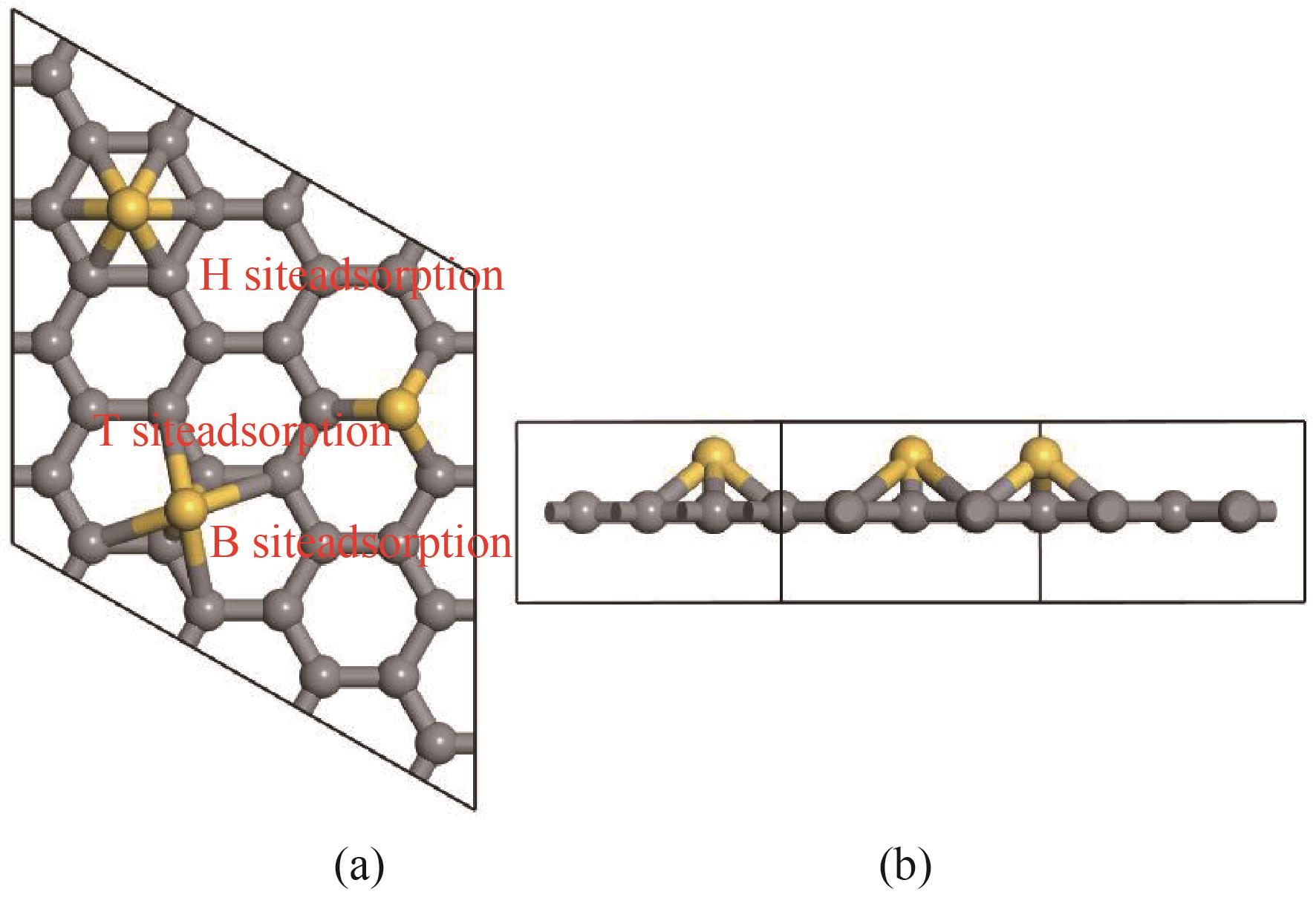
Fig. 1. The 4×4×1structures of graphene adsorbing metal atom at different adsorption sites (the gray balls represent carbon atoms, and the yellow ones represent adsorbed atoms) (a) top view, (b) side view
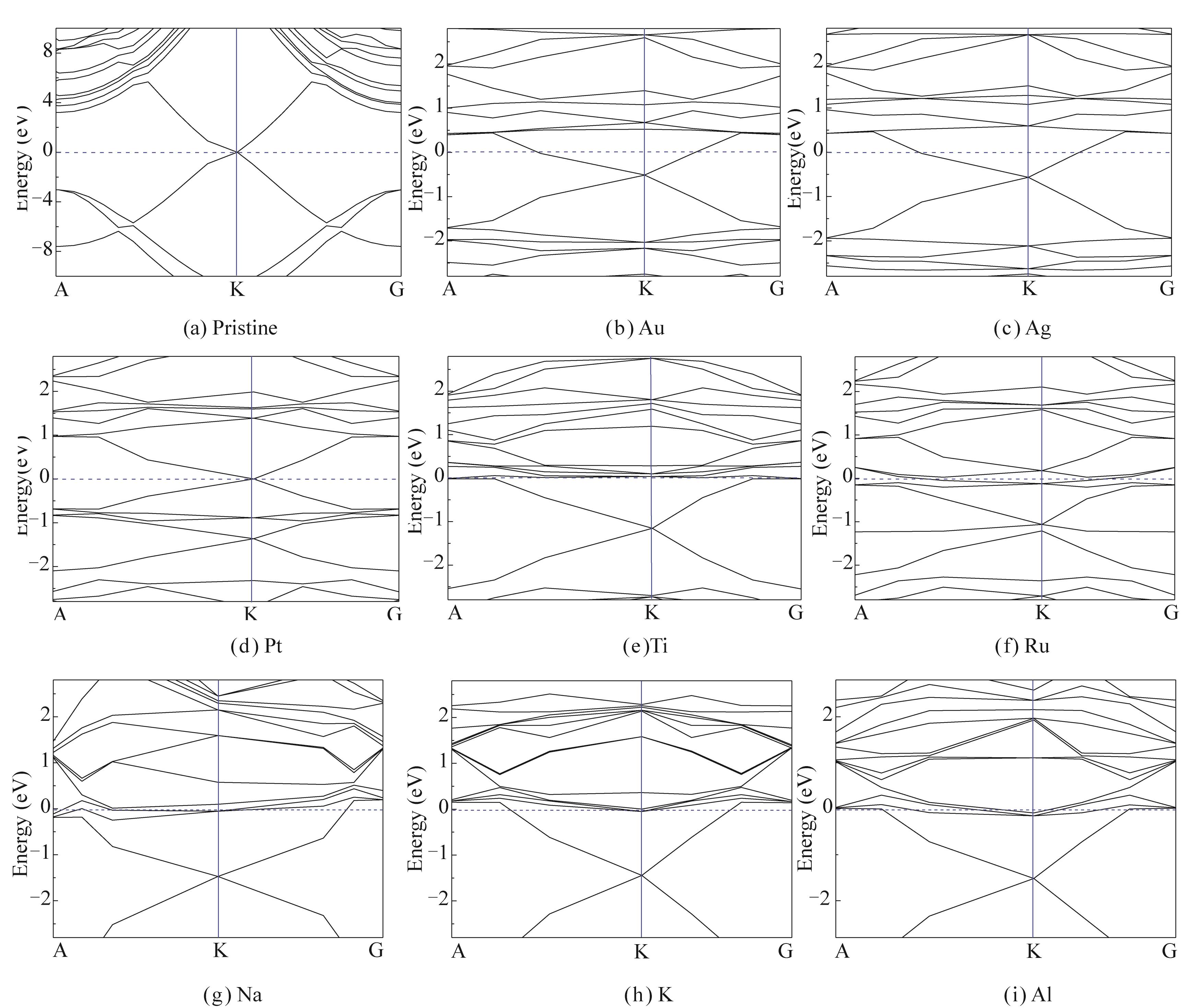
Fig. 2. Energy band structures of pristine graphene and graphene absorbed with different metal atoms( the blue solid lines represent K point of the Brillouin zone, the blue dashed line at 0 eVrepresents the Fermi level)
Fig. 3. PDOS of graphene absorbed with different metal atoms. Note: the black solid line at 0 eV represents the Fermi level
Fig. 4. Work function(Ф ) of graphene absorbed with different metal atoms
Fig. 5. Optical properties of graphene absorbed with different metal atoms. (a) real part of dielectric function, (b) imaginary part of dielectric function, (c) absorption, and (d) reflectivity
| ||||||||||||||||||||||||||||||||||||||||||||||
Table 1. The binding energies of metal atoms adsorbs at different sites of graphene (Eb / eV). Notes: H represents hollow site, T represents top site, and B represents bridge site.
|
Table 2. Number of transferred charges between the adatoms and graphene. Note: positive values represent that charges transfer from adatoms to graphene.
|
Table 3. The distance between the Fermi level and the Dirac cone after graphene adsorbs with different metal atoms (ΔEF / eV).
|
Table 4. The static real part of dielectric function ɛ1(0) of graphene absorbed with different metal atoms.

Set citation alerts for the article
Please enter your email address
© Copyright 2018-2021 | Chinese Laser Press. All Rights Reserved 沪ICP备15018463号-20