Abstract
Based on the first principles study, this paper investigates the control of the work function and optical properties of graphene absorbed with metal atoms. The work is conducted with eight different kinds of metal that are of most reactive (Na, K, and Al) and commonly used in experiments (Ti, Ag, Ru, Au, and Pt). The results show that all the adatoms loss electrons, resulting in the Dirac cone of graphene moves toward the direction of the low energy except for the adsorption of Ti and Ru atoms. The work functions of all the adsorption structures arelower than that of graphene. Particularly, the smaller work functions of Tiand Ru adsorption are observed due to the strong interaction between the Ti or Ru atom and graphene. Furthermore, the optical properties change greatly owing to the existence of adatoms. ?1(0) varies greatly with the different adsorption structures, the absorption intensity of the visible light and the infrared increased greatly.Introduction
Graphene, which has shown potential for use as a promising material in future nano-electronics due to its exceptional electric and transport properties, is sp2-bonded 2D sheet of carbon atoms arranged in a honeycomb pattern [1-2]. It exhibits an extraordinary electronic structure; a Dirac point of linear energy and momentum dispersion can be seen at the Fermi level (EF). This feature makes the electrons behave like massless relativistic particles and leads to interesting properties such as good electrical conductivity, ultra-high electron mobility, the quantum Hall effect at room temperature, and exceptional thermal and mechanical properties [3]. These outstanding performances can be used intransistors, single molecule gas detectors [4], integrated circuits [5], transparent conductive electrodes [6], biological devices [7], super capacitors [8], power electron couplers [9], and others.
For its application in optical devices, there are still many obstacles for graphene to overcome. The absorptivity of a single layer graphene is only 2.3%, the reflectivity of a single layer graphene is less than 0.1%. Partial visible light can be absorbed, while the absorption of light in the infrared energy region below visible light is extremely weak. The optical performance of graphene is far from our expectation. Recently, metal adatoms on graphene have been a topic of great interest since they can locally dope or modify its photoelectric properties. The work function of the metal-graphene contact is one of the critical factors that determine device performance, which can affect the current emitted in optoelectronics and maximize energy conversion efficiency in solar cells (as graphene electrodes) [10]. Graphene is considered to be a prospective conductive material whose performance depends strongly on the carrier injection efficiency through the contact. This means that the regulation of its work function is very important.
In recent years, considerable theoretical and experimental efforts have been made to tune the work function of graphene including through reaction with organic and inorganic molecules [11-14], chemical modification of the surface [15], metal doping [16-17], substrate orientation [18], self-assembled mono-layer formation [19], and the use of external electric fields [20]. Intercalation of different species has also been identified as a potential method for tuning the work function of few-layer graphene. In this paper, eight different metals that are of most reactive (Na, K, and Al) and commonly used in experiments (Ti, Ag, Ru, Au, and Pt) are selected to tune the photoelectric properties of graphene. The work function of graphene adsorbed with different metal atoms has been investigated through the metallic activity of adatoms and hybridization of electronic states between metal atoms and carbon atoms, the optical properties also has been investigated through the electron transition theory. Collectively, the results may well provide a very useful framework for the infrared application of graphene in optoelectronic devices.
1 Computational details
In this paper, the Cambridge Sequential Total Energy Package (CASTEP) module is adopted to calculate the electronic structure, work function, and optical properties of metal-adatom-doped graphene using first principles. Simulations are performed under generalized gradient approximation (GGA) with Perdew-Burke-Ernzerhof (PBE) exchange and correlation. In the process of structure optimization, 500 eV mesh cutoff energy is set for the expansion of plane wave basis sets and the convergence criteria are set to 5 × 10⁻⁶ eV for all systems. The Brillouin-zone (BZ) integration is calculated by the highly symmetric K points in the form of a Monkhorst-Pack 7 × 7 × 1 grid. The convergence criterion of the interaction force between atoms is set to 0.02 eV, and the stress convergence criterion in the crystal is set to 0.1 GPa. The convergence criterion of the maximal displacement of atoms is 1 × 10⁻³ Å. The Bader charge analyzing is adopted to calculate the charge transfer ΔQ. All calculations are carried in reciprocal space with C: 2s22p2, Au: 5d106s1, Ag: 4d105s1, Pt: 5d96s1, Ti: 3d24s2, Ru: 4d75s1, Na: 3s1, K: 4s1, and Al: 3s23p1 as the valence electrons.
2 Results and discussion
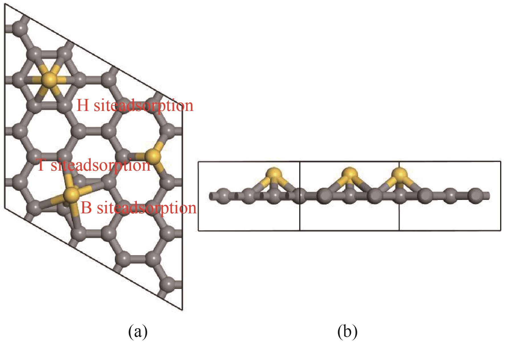
To adsorb metal atoms on the graphene surface, we construct a 4×4×1 supercell graphene structure. A 12 Å vacuum region perpendicular to the graphene surface is added, which is verified to be wide enough (based on the average electrostatic potential plot). Different kinds of adatoms can occupy the hollow (H) sites (at the center of a hexagon), the top (T) of carbon atoms, and bridges (B) between two carbon atoms. Figure 1 shows the 4×4×1structures of graphene sheet adsorbing metal atom (the structures shown have not been optimized) at the three adsorption sites, the height between adatoms and graphene is set to 3 Å. The graphene structures with adatoms occupying different sites are optimized, different adatoms prefer to occupy different sites. The best adsorption sites for the different adatoms will be discussed in the binding energy section below.

Figure 1.The 4×4×1structures of graphene adsorbing metal atom at different adsorption sites (the gray balls represent carbon atoms, and the yellow ones represent adsorbed atoms) (a) top view, (b) side view
The binding energy of the adatoms can be defined as:
where EG-nM is the total energy of the graphene sheet with metal, EG is the total energy of the pristine graphene sheet, EM is the total energy of the free metal adatom, and n corresponds to the number of adatoms. The binding energies of adatoms (Eb) that occupy different adsorption sites are shown in Table 1. The results show that all the binding energies of adatoms are negative, which illustrate that the adsorption sites are stable. From the table we can see that the metal atoms that commonly used in experiments (Ti, Ag, Ru, Au, and Pt) are prefer to occupy the B sites, while the most reactive atoms (Na, K, and Al) are prefer to occupy the H sites. The results of Na, K, and Al adsorption are similar to the Ref. 21. However, the properties of graphene will vary due to the different adsorption sites that occupied by the same adatom. Based on stability considerations, the following discussions are based on this optimal adsorption structure. One of the factors that affect the binding energy of adatoms is metal activity. In the case of Na, K, and Al, the small absolute values of binding energy mean that they are difficult to adsorb on graphene due to their activity, which are likely to desorb from the graphene sheet. Another factor that affects the binding energy is the ionization potential of adatoms. In the case of Au, Ag, and Pt, the higher ionization potential corresponds to the bigger binding energy, the affinity with carbon atoms of graphene is so weak that weak chemical interaction takes place. Charge transfer is another important feature in the adsorption process. The number of transferred charges is presented in Table 2. As seen, all the adatoms loss the electrons due to the fact that their electronegativity is smaller than that of carbon atoms. In the case of Ti, Ru, Na, and K adsorption structures, notable electrons transfer from adatoms to graphene, suggesting significant chemical interaction between the adatoms and graphene surfaces. For the Pt, Au, Ag, and Al adsorption structures, small number of charges transfer from adatoms to graphene, which implies that weak interactions occur between adatoms and graphene surfaces. The large charge transfer corresponds to strong interactions between the adatoms and graphene, resulting in high system stability. Furthermore, the mount of transferred electrons will directly affect the position of the Dirac cone relative to the Fermi levelin the energy band structure, which will be discussed in the energy band structure section below.
| Adsorption site | Adatoms |
|---|
| Au | Ag | Ti | Pt | Ru | Na | K | Al |
|---|
| Binding energy (Eb/eV) | H | -0.487 | -0469 | -0.626 | -1.014 | -0.198 | -0.105 | -0.321 | -0.178 |
| T | -1.735 | -1.529 | -0.851 | -2.204 | -0.954 | -0.081 | -0.304 | -0.135 |
| B | -2.433 | -1.815 | -1.017 | -2.243 | -1.259 | -0.047 | -0.232 | -0.094 |
Table 1. The binding energies of metal atoms adsorbs at different sites of graphene (Eb / eV). Notes: H represents hollow site, T represents top site, and B represents bridge site.
| Adatoms | Au | Ag | Ti | Pt | Ru | Na | K | Al |
|---|
| Number of transferred charges | 0.26 | 0.23 | 2.17 | 0.17 | 1.79 | 1.39 | 0.99 | 0.48 |
Table 2. Number of transferred charges between the adatoms and graphene. Note: positive values represent that charges transfer from adatoms to graphene.
Graphene has many interesting properties due to its Dirac cone. In the energy band structure of pristine graphene, the band gap is zero, the phenomenon that EF crosses the Dirac point at the K point in the Brillouin zone is shown in Fig. 2(a). Figures 2(b-i) represent the energy band structures of graphene absorbed with different metal atoms. From the figures we can see that the energy band structures are not changed for the graphene adsorbed with Na, K, Al, Ag, Au, and Pt, the Dirac cone has a shift with respect to EF however. The Dirac cone moves toward the direction of the low energy owing to the fact that the graphene surface gets electrons from the adatoms, the distance between the Fermi level. The distance between the Fermi level and the Dirac cone after graphene adsorbs with different metal atoms are shown in Table 3. In combination with Tables 2 and 3 we can see that ΔEF is closely related to the mount of transferred electrons. The notable transferred charge implies big ΔEF, while less transferred charge implies small ΔEF. The nature of the energy band structures mentioned above changes for the graphene adsorbed with Ti and Ru, the Dirac cone is completely lost. In the Ti and Ru adsorption structures, the strong interaction between graphene and metal adatoms is observed at the Fermi level, resulting in a strong hybridization between metal d- and graphene π- bands below and above EF. For the Ru adsorption structure, the split Dirac cone even can be seen.
Figure 2.Energy band structures of pristine graphene and graphene absorbed with different metal atoms( the blue solid lines represent K point of the Brillouin zone, the blue dashed line at 0 eVrepresents the Fermi level)
| Adatoms | Au | Ag | Ti | Pt | Ru | Na | K | Al |
|---|
| ΔEF/eV | 0.57 | 0.41 | - | 0.03 | - | 1.47 | 1.44 | 1.42 |
Table 3. The distance between the Fermi level and the Dirac cone after graphene adsorbs with different metal atoms (ΔEF / eV).
The relative shift and perturbation in the Dirac nature of the graphene absorbed with different metal atoms are highlighted in Fig.3 using the partial density of states (PDOS). From Fig.2 we can see that some impurity energy levels of metal atoms are superimposed on the energy band of graphene after the graphene absorbed with different metal atoms, and the change of energy level at the Fermi level will lead to the change of its properties. In Fig. 3, the orbital hybridization near the Fermi level between adatoms and C atoms is observed, which corresponds to the energy band structures in Fig. 2. The distance between the position that the orbital hybridization takes place and the Fermi energy level and the strength of the orbital hybridization determine the degree of interaction between the adsorbed atom and graphene, and thus the amount of transfer electrons. The closer the position of the orbital hybridization relative to the Fermi energy level and the higher the density of the states involved in the orbital hybridization, the stronger the interaction between the adsorbed atom and graphene, and the more transfer electrons. In Fig. 3(a), the 5d states of Au hybridize with the 2p states of C at the right of the Fermi level. Weak interaction between Au and graphene is observed, 0.26 charges transfer between them. The similar case for Ag adsorption structure, the 4d states of Ag hybridize with the 2p states of C at the right of the Fermi level, which also implies weak interactions between Ag and graphene, and 0.23 charges transfer between them. In Fig. 3(c), the 5d states of Pt hybridize with the 2p states of C at the right of the Fermi level. The weakest interaction between Pt and graphene corresponds to the fewest transfer charges, 0.17 charges transfer between them. In Fig.3(d), the 3d states of Ti hybridize with the 2p states of C below and above the Fermi level, the hybrid peak at the Fermi level is observed, which implies strong interactions between Ti and graphene, the metal-donated electrons are shared by the metal atoms and the interacting carbon atoms. The similar case for Ru adsorption structure, the 4d states of Ru hybridize with the 2p states of C below and above the Fermi level, the hybrid peak at the Fermi level is observed, which also implies strong interactions between Ru and graphene. In the Na and K adsorption structures, the 3s states of Na and 4s states of K hybridize with the 2p states of C below and above the Fermi level respectively, the hybrid peak at the right of the Fermi level is observed, which implies slightly strong interactions between adatoms and graphene, 1.47 and 1.44 charges transferfrom Na and K to graphene. The similar case for Al adsorbed graphene, the 3p states of Al hybridized with the 2p states of C below and above the Fermi level, the hybrid peak at the left of the Fermi level is observed. However, Al-graphene bonding is weak because electron transfer from Al to graphene is only 0.48, this result is similar to the Ref.21.
Figure 3.PDOS of graphene absorbed with different metal atoms. Note: the black solid line at 0 eV represents the Fermi level
The work function of any material can be defined as the energy required to remove an electron from the highest filled level in the Fermi distribution of a solid to vacuum at absolute zero. The work function of doped graphene is defined as the energy difference between the vacuum and Fermi energies. The calculated work function of intrinsic graphene is 4.32 eV and is very close to the experimentally measured work function of graphene which ranges between 4.4~4.5 eV (Ref.22-23). Figure 4 represents the work function of graphene absorbed with different adatoms. The results show that the work functions of all the adsorption structures are lower than that of intrinsic graphene, the difference of reduction degree can be seen obviously. In the case of Au, Ag, and Pt absorbed graphene, weak interactions between adatoms and graphene make their work functions smaller than that of the intrinsic graphene but bigger than other adsorption structures of graphene. For the Ti and Ru adsorbed graphene, the value of the work function correlates with the strong hybridization between metal atoms and carbon atoms at the Fermi level, the work function can be smaller than that of adsorption structures of graphene mentioned above. In the case of Na, K, and Al absorbed graphene, there is a strong correlation between work function and metallic activity, the more active adatom corresponds to the smaller work function of the adsorbed structure. In the case of K adsorption, the work function is 1.756 eV that is the minimum value due to its strongest activity, this result is close to experimental reported values.
Figure 4.Work function(Ф) of graphene absorbed with different metal atoms
Within the linear response range, the structure of the energy band of a solid and other kinds of spectral information can be obtained from the dielectric function, which associates the micro-physical process of inter-band transition with the electronic structure of the solid. In the dielectric function, the decline of the real part determines the peak value of the imaginary part, and the imaginary part represents the optical absorption intensity. Figures 5(a) and (b) represent the frequency-dependent real and imaginary parts of the dielectric function ɛ(ω) of the graphene absorbed with different adatoms (ɛ1(ω) represents the real part of the dielectric function, ɛ2(ω) represents its imaginary part). For pristine graphene, the static dielectric function ɛ1(0) is 6.56, the maximum value of the real part is 13.51 at an optical energy of 2.90 eV, and the minimum value is found to be -3.47 at an optical energy of 4.22 eV.With an increase in the optical energy, the real part decreases rapidly in the range 2.90∼4.22 eV, which indicates that the imaginary part increases rapidly in this range. However, fluctuation in the trend of the imaginary part is also observed at certain points over the whole optical energy range. The ɛ2(ω) of pure graphene is divided into two parts—0~8.43 eV in the low phonon energy region and above 8.43 eV in the high phonon energy region. The main peaks of ɛ2(ω) in the different phonon energy region correspond to the specific inter-band transition. Two main peaks in the low phonon energy region are observed in the graph of ɛ2(ω) at phonon energy of 3.59 eV and 6.74 eV, which correspond to the transition σ -π*. Three main peaks in the high energy region are observed in the graph of ɛ2(ω) at optical energies of 13.56, 15.56, and 20.63 eV, which correspond to the transition σ - σ*.
Figure 5.Optical properties of graphene absorbed with different metal atoms. (a) real part of dielectric function, (b) imaginary part of dielectric function, (c) absorption, and (d) reflectivity
The calculated static dielectric constants ɛ1(0) of the graphene absorbed with different adatoms are shown in Table 4, we can see that the ɛ1(0) varies greatly with the different adsorption structures, which prove that the optical properties of graphene are highly sensitive and tunable. In Fig. 5(b), the peaks in the high phonon energy region lost, the positions of the peaks in the high phonon energy region shifted to the lower phonon energy region. Meanwhile, the value of ɛ2(ω) that represent the transition σ - π* in the low phonon energy region increases for Au, Ag, Ti, and Ru adsorbed structures, while the opposite cases can be seen for the other adsorption structures. Combing Fig. 2, Fig. 3, and Fig. 5 we can know that the carrier transition barrier height is lowered by the introduction of impurity energy levels of metal atoms to the energy band of graphene, the transition peaks in the low phonon energy region mainly represent the transition between the energy levels of metal atoms and C atoms.
| Adatoms | pristine | Au | Ag | Ti | Pt | Ru | Na | K | Al |
|---|
| ɛ1(0) | 6.56 | 2.66 | 2.79 | 4.47 | 99.95 | 9.93 | 87.82 | 167.96 | 74.25 |
Table 4. The static real part of dielectric function ɛ1(0) of graphene absorbed with different metal atoms.
Figure 5(c) shows the absorption coefficients of the graphene absorbed with different adatoms. For pristine graphene, the maximum absorption coefficient is 47.88 μm-1 at an phonon energy of 16.11 eV in the high phonon energy region. The absorption edge begins at the optical energy of 1.24 eV, which corresponds to the transition threshold of σ -π*, but low absorption intensity is observed for the visible light (1.38~3.26 eV). After the adsorption of metal atoms on graphene surfaces, the intensity of the absorption spectrum decreased significantly, the absorption spectrum shrunk considerably in the high phonon energy region. The positions of the peaks in the low phonon energy region shifted to the lower phonon energy region containing the visible light and the following phonon energy region, which indicates that the absorption intensity of the visible light and the infrared light increases to some extent. For the Pt, Ti, Ru, Na, K, and Al absorbed graphene, new absorption peaks in the low phonon energy region containing the infrared light are observed , implying that the absorption intensity of the infrared light increased greatly. This change is attributed mainly to the presence of the impurity states of adatoms, thus providing a competing path for optical excitation so that electron-hole pairs form bound excitons (excitonic transition) and enhancing the light absorption in the low phonon energy region.
Figure 5(d) shows the reflectivity of the graphene absorbed with different adatoms. For pristine graphene, the curve is divided into two parts—0~7.77 eV in the low phonon energy region and above 7.77 eV in the high phonon energy region, the maximum reflectivity is 0.58 at phonon energy of 22.24 eV. After the adsorption of metal atoms on graphene surfaces, the reflection spectrum shrinks considerably in the high phonon energy region. For the graphene absorbed with Au, Ag, Ti, and Ru, the intensity of peaks decreased significantly, while the intensity of peaks increased slightly for the Pt, Na, K, and Al adsorption structures. One of the factors that affect the position of reflection peaks and the change of its peak values is the position of the orbital hybridization between metal atoms and graphene and the DOS of electrons involved in the hybridization. In the case of Ti, Ru, Na, K, and Al absorbed graphene, the reflection peaks at the 0eV correspond to the orbital hybridization below and above the Fermi level.
3 Conclusions
In summary, eight different metals that are of most reactive (Na, K, and Al) and commonly used in experiments (Ti, Ag, Ru, Au, and Pt) are adopted to tune the work function and photoelectricity properties of graphene through the first principle calculations. Based on the analysis of adsorption energies, energy band structures, PDOS, electron transfer, work function, dielectric function, adsorption coefficient, and reflectivity, the reduction of the work function and the modulation mechanisms of optical properties are well-understood. It is seen that the transfer of electrons from metal atoms to graphene brings the Fermi energy level higher than the Dirac cone due to the activity of adatoms (Na, K, and Al) and weak interactions between adatoms (Ag, Au, and Pt) and graphene, which decides the magnitude of the work function. The strong interaction of the Ti or Ru atoms with graphene makes the electrically neutral Dirac point disappeared and results in a smaller work function. Since there is a relationship between electronic structures and optical properties, the absorption intensity of the visible light and the infrared increased greatly than that of intrinsic graphene, which is suitable for the application of infrared field.
References
[1] A K Geim, K S Novoselov. The rise of graphene. Nature Materials, 6, 183(2007).
[2] X Wang, Y Ouyang, X Li. Room-temperature all-semiconducting sub-10-nm graphene nanoribbon field-effect transistors. Physical Review Letters, 100, 206803(2008).
[3] Y M Lin, C Dimitrakopoulos, K A Jenkins. 100-GHz transistors from wafer-scale epitaxial graphene. Science, 327, 662(2010).
[4] F Schedin, A K Geim, S V Morozov. Detection of individual gas molecules adsorbed on graphene. Nature Materials, 6, 652-655(2007).
[5] J H Chen, M Ishigami, C Jang. Printed graphene circuits. Advanced Materials, 19, 3623-3627(2007).
[6] X Wang, L Zhi, K Müllen. Transparent, conductive graphene electrodes for dye-sensitized solar cells. Nano Letters, 8, 323-327(2008).
[7] N Mohanty, V Berry. Graphene-based single-bacterium resolution biodevice and DNA transistor: interfacing graphene derivatives with nanoscale and microscale biocomponents. Nano Letters, 8, 4469-4476(2008).
[8] M D Stoller, S Park, Y Zhu. Graphene-based ultracapacitors. Nano Letters, 8, 3498-3502(2008).
[9] J S Bunch, A M Van Der Zande, S S Verbridge. Electromechanical resonators from graphene sheets. Science, 315, 490-493(2007).
[10] F Xia, T Mueller, R Golizadeh-Mojarad. Photocurrent imaging and efficient photon detection in a graphene transistor. Nano Letters, 9, 1039-1044(2009).
[11] K P Loh, Q Bao, P K Ang. The chemistry of graphene. Journal of Materials Chemistry, 20, 2277-2289(2010).
[12] R Garg, N Dutta, N Choudhury. Work function engineering of graphene. Nanomaterials, 4, 267(2014).
[13] Y X Yu. A dispersion-corrected DFT study on adsorption of battery active materials anthraquinone and its derivatives on monolayer graphene and h-BN. Journal of Materials Chemistry A, 2, 8910-8917(2014).
[14] Y X Yu. 16267-16275. ACS Applied Materials & Interfaces, 6(2014).
[15] Y Shi, K K Kim, A Reina. Work function engineering of graphene electrode via chemical doping. ACS Nano, 4, 2689-2694(2010).
[16] A Benayad, Shin H -J, H K Park. Controlling work function of reduced graphite oxide with Au-ion concentration. Chemical Physics Letters, 475, 91-95(2009).
[17] B G Wang, S Günther, J Wintterlin. Periodicity, work function and reactivity of graphene on Ru(0001) from first principles. New Journal of Physics(12).
[18] Y Murata, E Starodub, B B Kappes. Orientation-dependent work function of graphene on Pd(111). Applied Physics Letters, 97, 14(2010).
[19] J Park, W H Lee, S Huh. Work-function engineering of graphene electrodes by self-assembled monolayers for high-performance organic field-effect transistors. Journal of Physical Chemistry Letters, 2, 841-845(2010).
[20] R Gholizadeh, Y X Yu. 28274-28282. The Journal of Physical Chemistry C, 118(2014).
[21] M Legesse, F E Mellouhi, E T Bentria. Reduced work function of graphene by metal adatoms. Applied Surface Science, 394, 98-107(2017).
[22] S Ryu, L Liu, S Berciaud. Atmospheric oxygen binding and hole doping in deformed graphene on a SiO₂ substrate. Nano Letters, 10, 4944-4951(2010).
[23] J H Kim, J H Hwang, J Suh. Work function engineering of single layer graphene by irradiation-induced defects. Applied Physics Letters, 103, 171604(2013).