• Photonics Research
  • Vol. 8, Issue 12, 1949 (2020)
Linqing Zhuo1, Pengpeng Fan1, Shuang Zhang1, Yuansong Zhan2, Yanmei Lin1, Yu Zhang1, Dongquan Li2, Zhen Che1, Wenguo Zhu3、5, Huadan Zheng2, Jieyuan Tang2, Jun Zhang1, Yongchun Zhong3, Wenxiao Fang4, Guoguang Lu4, Jianhui Yu1、*, and Zhe Chen2、3
Author Affiliations
  • 1Key Laboratory of Optoelectronic Information and Sensing Technologies of Guangdong Higher Education Institutes, Department of Optoelectronic Engineering, Jinan University, Guangzhou 510632, China
  • 2Engineering Research Center on Visible Light Communication of Guangdong Province, Department of Optoelectronic Engineering, Jinan University, Guangzhou 510632, China
  • 3Key Laboratory of Visible Light Communications of Guangzhou, Jinan University, Guangzhou 510632, China
  • 4Science and Technology on Reliability Physics and Application of Electronic Component Laboratory, China Electronic Product Reliability and Environmental Testing Research Institute, Guangzhou 510610, China
  • 5e-mail: zhuwg88@163.com
  • show less
    DOI: 10.1364/PRJ.402108 Cite this Article Set citation alerts
    Linqing Zhuo, Pengpeng Fan, Shuang Zhang, Yuansong Zhan, Yanmei Lin, Yu Zhang, Dongquan Li, Zhen Che, Wenguo Zhu, Huadan Zheng, Jieyuan Tang, Jun Zhang, Yongchun Zhong, Wenxiao Fang, Guoguang Lu, Jianhui Yu, Zhe Chen. High-performance fiber-integrated multifunctional graphene-optoelectronic device with photoelectric detection and optic-phase modulation[J]. Photonics Research, 2020, 8(12): 1949 Copy Citation Text show less
    (a) Schematic of optic-phase modulation and photoelectric detection by the AFGD, where two microstrip electrodes are fabricated on an SPF deposited with a hybrid graphene/PB/PMMA film; (b) atomic force microscopy (AFM) image of hybrid graphene/PB/PMMA film. The inset shows the cross sections of graphene/PB/PMMA film, indicating the thickness of the film being 245.2 nm. (c) The input (pink spheres) and output (blue spheres) optical power of AFGD changing with the incident polarization angle.
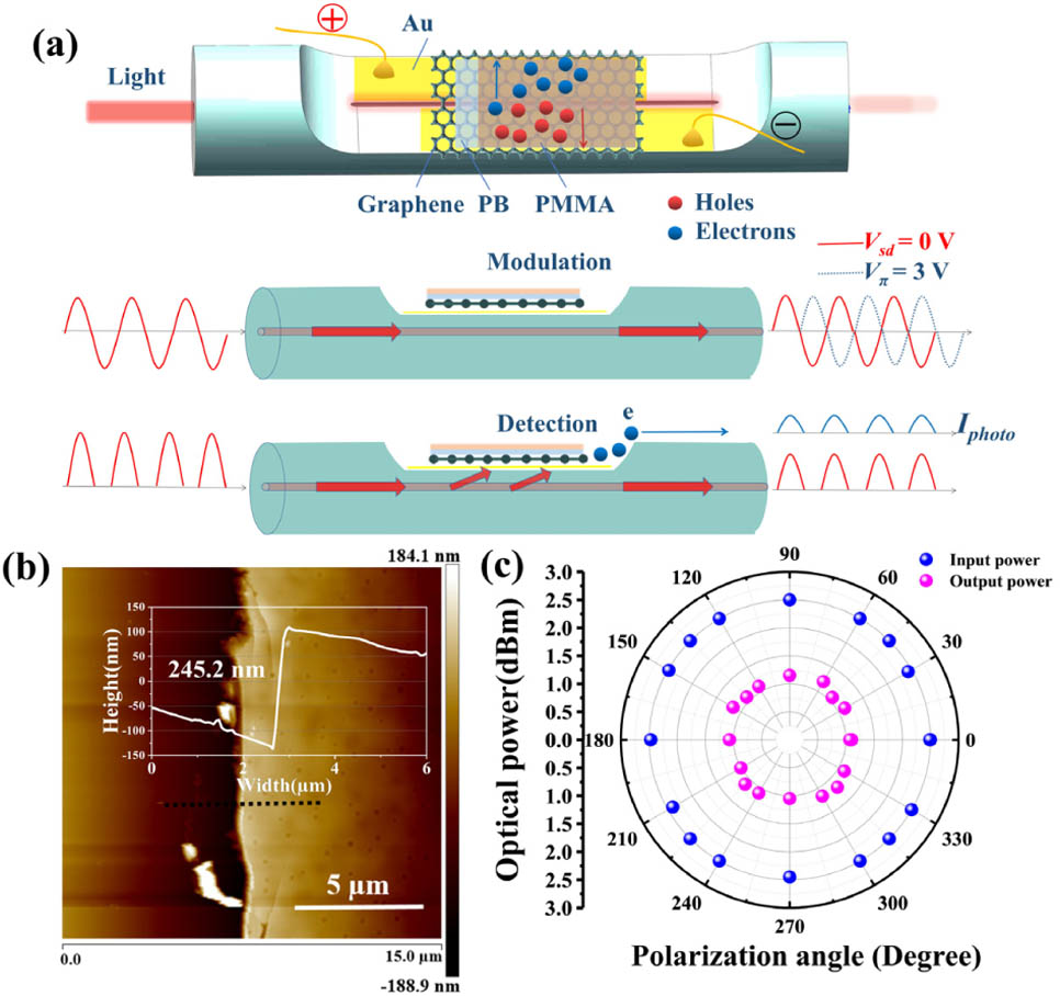
    Fig. 1. (a) Schematic of optic-phase modulation and photoelectric detection by the AFGD, where two microstrip electrodes are fabricated on an SPF deposited with a hybrid graphene/PB/PMMA film; (b) atomic force microscopy (AFM) image of hybrid graphene/PB/PMMA film. The inset shows the cross sections of graphene/PB/PMMA film, indicating the thickness of the film being 245.2 nm. (c) The input (pink spheres) and output (blue spheres) optical power of AFGD changing with the incident polarization angle.
    (a) Normalized intensities along the y axis for the cases with and without PB/PMMA. Insets show the enlarged TE mode intensity distribution at position of graphene. (b) Transmission spectra of bare SPF (pink line), SPF covered with graphene (blue line), and SPF covered with hybrid graphene/PB/PMMA film (red line).
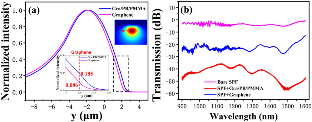
    Fig. 2. (a) Normalized intensities along the y axis for the cases with and without PB/PMMA. Insets show the enlarged TE mode intensity distribution at position of graphene. (b) Transmission spectra of bare SPF (pink line), SPF covered with graphene (blue line), and SPF covered with hybrid graphene/PB/PMMA film (red line).
    (a) Photocurrent and (c) responsivity of the AFGD as a function of bias voltage for different light powers at 1550 nm; (b) photocurrent and (d) responsivity of the AFGD changing with the light power at VBS=0.1 V, where both axes are in the logarithmic scale; (b) shows a broad LDR of AFGD in weak light. (e) Schematic of electron–hole pair excitation in graphene for weak light; (f) schematic of graphene saturated absorption; (g) polarization-independent property of the generated photocurrent of the AFGD for 1550 nm incident light (Pin=2.5 dBm, VBS=0.3 V).
    Fig. 3. (a) Photocurrent and (c) responsivity of the AFGD as a function of bias voltage for different light powers at 1550 nm; (b) photocurrent and (d) responsivity of the AFGD changing with the light power at VBS=0.1  V, where both axes are in the logarithmic scale; (b) shows a broad LDR of AFGD in weak light. (e) Schematic of electron–hole pair excitation in graphene for weak light; (f) schematic of graphene saturated absorption; (g) polarization-independent property of the generated photocurrent of the AFGD for 1550 nm incident light (Pin=2.5  dBm, VBS=0.3  V).
    (a) Photocurrent and (b) responsivity of the AFGD as a function of light power at 980 nm (red lines), 1310 nm (pink lines), 1550 nm (green lines), and 1610 nm (blue lines) at residual thickness of 68 μm (VBS=0.1 V); (c) responsivity changing with the residual thickness at 1550 nm (VBS=0.3 V, Pin=69 pW); (d) simulated absorption changing with the residual thickness. The insets in (c) show the macroscopic images of the cross section of SPFs. The insets in (d) show the intensity distributions of the fiber modes of SPFs.
    Fig. 4. (a) Photocurrent and (b) responsivity of the AFGD as a function of light power at 980 nm (red lines), 1310 nm (pink lines), 1550 nm (green lines), and 1610 nm (blue lines) at residual thickness of 68 μm (VBS=0.1  V); (c) responsivity changing with the residual thickness at 1550 nm (VBS=0.3  V, Pin=69  pW); (d) simulated absorption changing with the residual thickness. The insets in (c) show the macroscopic images of the cross section of SPFs. The insets in (d) show the intensity distributions of the fiber modes of SPFs.
    Air stability characterization. (a) The photocurrent and (b) responsivity tested as fabricated and 6 months later, at 1550 nm at room temperature (VBS=0.1 V).
    Fig. 5. Air stability characterization. (a) The photocurrent and (b) responsivity tested as fabricated and 6 months later, at 1550 nm at room temperature (VBS=0.1  V).
    (a) Dark current waveform of the AFGD with the source-drain voltage of VSD=0.3 V and the sampling frequency of 1.8 kHz; (b) analysis of noise spectral density of the AFGD based on the dark current waveform measured in (a).
    Fig. 6. (a) Dark current waveform of the AFGD with the source-drain voltage of VSD=0.3  V and the sampling frequency of 1.8 kHz; (b) analysis of noise spectral density of the AFGD based on the dark current waveform measured in (a).
    (a) Time-dependent photocurrent over eight-period on–off operation at 1550 nm; (b) the enlarged view of photocurrent shows the response time is ∼93 ms (VSD=1 mV). (c) Comparison of the responsivity and operation speed for the AFGD with some of the high-performance pure graphene photodetectors reported in the literature [12,24,26–32" target="_self" style="display: inline;">–32]; (d) exponential attenuation of the photocurrent Iph when there is no optical signal.
    Fig. 7. (a) Time-dependent photocurrent over eight-period on–off operation at 1550 nm; (b) the enlarged view of photocurrent shows the response time is 93  ms (VSD=1  mV). (c) Comparison of the responsivity and operation speed for the AFGD with some of the high-performance pure graphene photodetectors reported in the literature [12,24,2632" target="_self" style="display: inline;">32]; (d) exponential attenuation of the photocurrent Iph when there is no optical signal.
    (a) Experimental setup of the MZI-based graphene phase modulator. OC1 and OC2, 50:50 optical fiber coupler; VOA, variable optical attenuator. (b) Interferometric spectra at output 1 for the bias voltage being 0 V (blue dashed line) and 6 V (red solid line); (c) phase shift and temperature rise versus the bias voltage; (d) transmission power varies with a square bias voltage signal; in situ infrared thermograms of AFGD at (e) 0 V and (f) 5 V.
    Fig. 8. (a) Experimental setup of the MZI-based graphene phase modulator. OC1 and OC2, 50:50 optical fiber coupler; VOA, variable optical attenuator. (b) Interferometric spectra at output 1 for the bias voltage being 0 V (blue dashed line) and 6 V (red solid line); (c) phase shift and temperature rise versus the bias voltage; (d) transmission power varies with a square bias voltage signal; in situ infrared thermograms of AFGD at (e) 0 V and (f) 5 V.
    (a) AFM image of graphene/PMMA film; (b) cross section of graphene/PMMA film from the dashed line shown in AFM image; the thickness of the film is 203.6 nm.
    Fig. 9. (a) AFM image of graphene/PMMA film; (b) cross section of graphene/PMMA film from the dashed line shown in AFM image; the thickness of the film is 203.6 nm.
    Source-drain current I as a function of the back-gate voltage Vg; VSD=10 mV.
    Fig. 10. Source-drain current I as a function of the back-gate voltage Vg; VSD=10  mV.
    WaveguideMaterialDetectivity (Jones)Response TimeWavelengthResponsivityNEP (W·Hz1/2)References
    MicrofiberGraphene1500–1600 nm2.81 mA/W1×109[6]
    CSPFGraphene81 ms, 77 msNear-infrared0.44 A/W[12]
    Fiber end faceCsPbBr3-graphene8.6×10103.1 s, 24.2 s400 nm2×104 A/W3.9×1016[4]
    SPFGraphene3.29×101193 ms, 98 ms980–1610 nm1.5×107 A/W1.4×1015This work
    Table 1. Comparison of the Performance of the Fiber Waveguide Photodetectors
    Linqing Zhuo, Pengpeng Fan, Shuang Zhang, Yuansong Zhan, Yanmei Lin, Yu Zhang, Dongquan Li, Zhen Che, Wenguo Zhu, Huadan Zheng, Jieyuan Tang, Jun Zhang, Yongchun Zhong, Wenxiao Fang, Guoguang Lu, Jianhui Yu, Zhe Chen. High-performance fiber-integrated multifunctional graphene-optoelectronic device with photoelectric detection and optic-phase modulation[J]. Photonics Research, 2020, 8(12): 1949
    Download Citation