• Advanced Photonics
  • Vol. 4, Issue 2, 024002 (2022)
Lingqi Li1, Weijin Kong1, and Feng Chen2、*
Author Affiliations
  • 1Qingdao University, College of Physics Science, Center for Marine Observation and Communications, Qingdao, China
  • 2Shandong University, School of Physics, State Key Laboratory of Crystal Materials, Jinan, China
  • show less
    DOI: 10.1117/1.AP.4.2.024002 Cite this Article Set citation alerts
    Lingqi Li, Weijin Kong, Feng Chen. Femtosecond laser-inscribed optical waveguides in dielectric crystals: a concise review and recent advances[J]. Advanced Photonics, 2022, 4(2): 024002 Copy Citation Text show less
    Basic geometries of laser writing of waveguides: (a) single-line, (b) double-line, (c) depressed-cladding, and (d) optical-lattice-like configurations. The dark (gray) regions represent the laser-induced tracks.
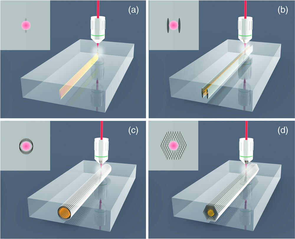
    Fig. 1. Basic geometries of laser writing of waveguides: (a) single-line, (b) double-line, (c) depressed-cladding, and (d) optical-lattice-like configurations. The dark (gray) regions represent the laser-induced tracks.
    Optical microscope images of laser-induced tracks with (a) different pulse energies and (b) scanning velocity in LiTaO3 crystal. (c) Different refractive index change profiles from positive to negative, depending on the propagation wavelength in ZnSe crystal. Image (c) is reproduced with permission from Ref. 103, Creative Commons Attribution License (CC-BY).
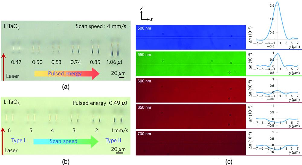
    Fig. 2. Optical microscope images of laser-induced tracks with (a) different pulse energies and (b) scanning velocity in LiTaO3 crystal. (c) Different refractive index change profiles from positive to negative, depending on the propagation wavelength in ZnSe crystal. Image (c) is reproduced with permission from Ref. 103, Creative Commons Attribution License (CC-BY).
    (a) Microscope images of tracks with different pulse energies and scanning rates in Nd:YVO4. (b) Influence of different laser polarizations on the tracks and modal profiles in Nd:YAP, perpendicular to the scans (No. 1) and parallel to the scans (No. 2), respectively. Images reprinted from Ref. 75, © 2016 The Optical Society (OSA). (c) Optical images of tracks as the laser writing along different crystalline orientations in Nd:GdVO4. (d) Laser-induced multifoci in LiTaO3, corresponding horizontal waveguides, and modal profiles. Reprinted with permission from Ref. 109, © 2019 IEEE.
    Fig. 3. (a) Microscope images of tracks with different pulse energies and scanning rates in Nd:YVO4. (b) Influence of different laser polarizations on the tracks and modal profiles in Nd:YAP, perpendicular to the scans (No. 1) and parallel to the scans (No. 2), respectively. Images reprinted from Ref. 75, © 2016 The Optical Society (OSA). (c) Optical images of tracks as the laser writing along different crystalline orientations in Nd:GdVO4. (d) Laser-induced multifoci in LiTaO3, corresponding horizontal waveguides, and modal profiles. Reprinted with permission from Ref. 109, © 2019 IEEE.
    Schematic diagram of direct laser-written cladding waveguides (a) with an ellipsoidal focal spot and (b) with a slit-shaped beam focus. Images (a), (b), and (g) are reprinted with permission from Ref. 40, © 2017 OSA. (c) The phase mask for writing horizontal lines. Microscope image of (d) horizontal tracks, (e) waveguide, and (f) near-field profiles. Images (c)–(f) are reproduced with permission from Ref. 42, CC-BY. (g) Schematic plot of single-scan cladding waveguides utilizing a longitudinal ring-shaped focal field. (h) Calculated 3D isosurface, (i) phase mask, and (j) simulated focal intensity profile. (k) Microscope image and (l), (m) corresponding modal profiles. Images (h)–(m) are reprinted with permission from Ref. 118, © 2019 Chinese Laser Press (CLP).
    Fig. 4. Schematic diagram of direct laser-written cladding waveguides (a) with an ellipsoidal focal spot and (b) with a slit-shaped beam focus. Images (a), (b), and (g) are reprinted with permission from Ref. 40, © 2017 OSA. (c) The phase mask for writing horizontal lines. Microscope image of (d) horizontal tracks, (e) waveguide, and (f) near-field profiles. Images (c)–(f) are reproduced with permission from Ref. 42, CC-BY. (g) Schematic plot of single-scan cladding waveguides utilizing a longitudinal ring-shaped focal field. (h) Calculated 3D isosurface, (i) phase mask, and (j) simulated focal intensity profile. (k) Microscope image and (l), (m) corresponding modal profiles. Images (h)–(m) are reprinted with permission from Ref. 118, © 2019 Chinese Laser Press (CLP).
    (a) Schematic design of a waveguide-integrated LiQPM grating; (b) SH microscope image of LiQPM grating and waveguide; and (c) helical grating structure. Microscope image of the helical structure: (d) the front face and (e) top view. Images reprinted with permission from Ref. 43, © 2020 OSA.
    Fig. 5. (a) Schematic design of a waveguide-integrated LiQPM grating; (b) SH microscope image of LiQPM grating and waveguide; and (c) helical grating structure. Microscope image of the helical structure: (d) the front face and (e) top view. Images reprinted with permission from Ref. 43, © 2020 OSA.
    (a) Microscope images of hollow optical-lattice-like structures at different etching times in YAG crystal. (b) Before polished and (c) after polished. Near-field modal profiles at 4 μm along (d) TM and (e) TE polarization, respectively. Images reproduced with permission from Ref. 129, © 2020 CLP.
    Fig. 6. (a) Microscope images of hollow optical-lattice-like structures at different etching times in YAG crystal. (b) Before polished and (c) after polished. Near-field modal profiles at 4  μm along (d) TM and (e) TE polarization, respectively. Images reproduced with permission from Ref. 129, © 2020 CLP.
    (a) Microscope images and modal profiles of tailored multiline waveguides in a LiNbO3 crystal, reproduced with permission from Ref. 91, © 2018 Elsevier. (b) Ring-shaped waveguide based on type-I modification in a BGO crystal, reprinted with permission from Ref. 136, © 2017 OSA. (c) Polarization engineering for dual-line waveguides in a LiNbO3 crystal, reproduced with permission from Ref. 167, © 2020 Elsevier. (d) The “ear-like” waveguide in Nd:YAG crystal, reprinted with permission from Ref. 168, © 2021 OSA. (e) Double-cladding waveguide in Nd:YVO4 crystal, reprinted with permission from Ref. 169, © 2019 OSA.
    Fig. 7. (a) Microscope images and modal profiles of tailored multiline waveguides in a LiNbO3 crystal, reproduced with permission from Ref. 91, © 2018 Elsevier. (b) Ring-shaped waveguide based on type-I modification in a BGO crystal, reprinted with permission from Ref. 136, © 2017 OSA. (c) Polarization engineering for dual-line waveguides in a LiNbO3 crystal, reproduced with permission from Ref. 167, © 2020 Elsevier. (d) The “ear-like” waveguide in Nd:YAG crystal, reprinted with permission from Ref. 168, © 2021 OSA. (e) Double-cladding waveguide in Nd:YVO4 crystal, reprinted with permission from Ref. 169, © 2019 OSA.
    (a) Fabrication and 3D schematic diagram of Y-splitters based on rectangular cladding geometry in Ti:sapphire crystal, (b) microscope image of 1-deg branching angle, and (c) intensity distributions at 1064 nm. Images (a)–(c) are reproduced with permission from Ref. 181, © 2018 Elsevier. Microscope images of Y-branch with circular cladding structure (d) in top view and (e) in cross section, as well as modal profiles of two arms. Images (d) and (e) are reproduced with permission from Ref. 179, © 2017 Elsevier. (f) 3D beam-splitting structures in a LiNbO3 crystal, reprinted with permission from Ref. 182, © 2018 Optica.
    Fig. 8. (a) Fabrication and 3D schematic diagram of Y-splitters based on rectangular cladding geometry in Ti:sapphire crystal, (b) microscope image of 1-deg branching angle, and (c) intensity distributions at 1064 nm. Images (a)–(c) are reproduced with permission from Ref. 181, © 2018 Elsevier. Microscope images of Y-branch with circular cladding structure (d) in top view and (e) in cross section, as well as modal profiles of two arms. Images (d) and (e) are reproduced with permission from Ref. 179, © 2017 Elsevier. (f) 3D beam-splitting structures in a LiNbO3 crystal, reprinted with permission from Ref. 182, © 2018 Optica.
    (a) Schematic illustration of 1×4 beam splitting and ring-shaped transformation based on photonic-lattice-like structures. Image (a) is reproduced from Ref. 102. (b) Measured evolution of ring-shaped transformation in a Nd:YAG crystal. The scale bar is 50 μm. (c) Prototype design and microscope images of 1×3 beam splitters in a LiNbO3 crystal, (d) measured and (e) simulated modal profile. Images (c)–(e) are reprinted with permission from Ref. 145, © 2016 IEEE.
    Fig. 9. (a) Schematic illustration of 1×4 beam splitting and ring-shaped transformation based on photonic-lattice-like structures. Image (a) is reproduced from Ref. 102. (b) Measured evolution of ring-shaped transformation in a Nd:YAG crystal. The scale bar is 50  μm. (c) Prototype design and microscope images of 1×3 beam splitters in a LiNbO3 crystal, (d) measured and (e) simulated modal profile. Images (c)–(e) are reprinted with permission from Ref. 145, © 2016 IEEE.
    (a) Microscope images in top view, (b) end-face of polarization beam splitters, and (c) modal profiles along n0, ne, and circular polarizations, respectively. Images (a)–(c) are reprinted with permission from Ref. 184, © 2020 IEEE. (d) Schematic plot and microscope images of 3D polarizer. (c) Modal profiles at different polarizations. Images (d) and (e) are reprinted with permission from Ref. 167, © 2020 IEEE.
    Fig. 10. (a) Microscope images in top view, (b) end-face of polarization beam splitters, and (c) modal profiles along n0, ne, and circular polarizations, respectively. Images (a)–(c) are reprinted with permission from Ref. 184, © 2020 IEEE. (d) Schematic plot and microscope images of 3D polarizer. (c) Modal profiles at different polarizations. Images (d) and (e) are reprinted with permission from Ref. 167, © 2020 IEEE.
    (a) Microscopic pictures of a tapered cladding waveguide in a Nd:YAG crystal and (b) modal profiles at the input radii of 24 μm and output of 6 μm, respectively. (c) Modal profiles of a straight and tapered waveguide at the same output radii from an incident LED light, reproduced with permission from Ref. 185, CC-BY. (d) Prototype of depressed-cladding 3D waveguide arrays. (e) Optical micrographs at the output face for different separations between the central and adjacent waveguides. Images (d) and (e) are reprinted with permission from Ref. 186, © 2017 IEEE.
    Fig. 11. (a) Microscopic pictures of a tapered cladding waveguide in a Nd:YAG crystal and (b) modal profiles at the input radii of 24  μm and output of 6  μm, respectively. (c) Modal profiles of a straight and tapered waveguide at the same output radii from an incident LED light, reproduced with permission from Ref. 185, CC-BY. (d) Prototype of depressed-cladding 3D waveguide arrays. (e) Optical micrographs at the output face for different separations between the central and adjacent waveguides. Images (d) and (e) are reprinted with permission from Ref. 186, © 2017 IEEE.
    (a), (b) Geometry and cross-section design in the interaction region of the 3×3 directional coupler in a Tm3+:YAG crystal. (c), (d) Top and output view microscope images and (e) output intensity distribution. Images (a)–(e) are reproduced with permission from Ref. 187, CC-BY. (f) Schematic plot of 2×2 directional coupler integrated with 3D microelectrodes in a LiNbO3 crystal. (g) Output intensity profiles with different voltages. Images (f) and (g) are reprinted with permission from Ref. 118, © 2019 CLP.
    Fig. 12. (a), (b) Geometry and cross-section design in the interaction region of the 3×3 directional coupler in a Tm3+:YAG crystal. (c), (d) Top and output view microscope images and (e) output intensity distribution. Images (a)–(e) are reproduced with permission from Ref. 187, CC-BY. (f) Schematic plot of 2×2 directional coupler integrated with 3D microelectrodes in a LiNbO3 crystal. (g) Output intensity profiles with different voltages. Images (f) and (g) are reprinted with permission from Ref. 118, © 2019 CLP.
    Complex waveguide laser modal profiles at 1 μm: (a), (b) Y-branches, (c) 1×4-branch, (d) ring-shaped transformation, and (e) optical-lattice-like. Images (a) and (d) are reproduced with permission from Ref. 100. Images (b) and (c) are reprinted with permission from Ref. 101, © 2016 IEEE. Image (e) is reprinted with permission from Ref. 75, © 2016 OSA. (f) Schematic illustration of the fabrication process of an S-curved waveguide, (g) laser spectra of dual-wavelengths at 1064 and 1079 nm, and (h) RF spectrum of modelocking at 31.69 GHz. Images (f)–(h) are reprinted with permission from Ref. 159, © 2020 IEEE.
    Fig. 13. Complex waveguide laser modal profiles at 1  μm: (a), (b) Y-branches, (c) 1×4-branch, (d) ring-shaped transformation, and (e) optical-lattice-like. Images (a) and (d) are reproduced with permission from Ref. 100. Images (b) and (c) are reprinted with permission from Ref. 101, © 2016 IEEE. Image (e) is reprinted with permission from Ref. 75, © 2016 OSA. (f) Schematic illustration of the fabrication process of an S-curved waveguide, (g) laser spectra of dual-wavelengths at 1064 and 1079 nm, and (h) RF spectrum of modelocking at 31.69 GHz. Images (f)–(h) are reprinted with permission from Ref. 159, © 2020 IEEE.
    (a) Waveguide-integrated 3D LiQPM scheme, one period, two periods, and four periods in a LiNbO3 crystal. (b) Simultaneous SHG of four wavelengths and the fundamental and second harmonic modal profiles of a single period. Images (a) and (b) are reprinted with permission from Ref. 43, © 2020 OSA. (c) Experimental setup of the ultraviolet SHG process using LiQPM structure in a quartz crystal and (d) the SHG response signal of 177.3 nm. Images (c) and (d) are reproduced with permission from Ref. 124, CC-BY. (e) Schematic diagram of femtosecond laser-written cladding waveguide in a fan-out PPSLT crystal and (f) temperature tuning curves of seven waveguides with different poling periods. Images (e) and (f) are reprinted with permission from Ref. 148, © 2019 OSA.
    Fig. 14. (a) Waveguide-integrated 3D LiQPM scheme, one period, two periods, and four periods in a LiNbO3 crystal. (b) Simultaneous SHG of four wavelengths and the fundamental and second harmonic modal profiles of a single period. Images (a) and (b) are reprinted with permission from Ref. 43, © 2020 OSA. (c) Experimental setup of the ultraviolet SHG process using LiQPM structure in a quartz crystal and (d) the SHG response signal of 177.3 nm. Images (c) and (d) are reproduced with permission from Ref. 124, CC-BY. (e) Schematic diagram of femtosecond laser-written cladding waveguide in a fan-out PPSLT crystal and (f) temperature tuning curves of seven waveguides with different poling periods. Images (e) and (f) are reprinted with permission from Ref. 148, © 2019 OSA.
    (a), (b) Microscope image and near-field intensity profile of a type-II waveguide in a Pr3+:Y2SiO5 crystal. (c) Energy-level structure of H34 ground and D12 excited manifolds. (d) Light-storage experiments using the AFC protocol. Images (a)–(d) are reproduced with permission from Ref. 229, © 2016 American Physical Society (APS). (e), (f) End-face and top-view microscope images of type I and type II waveguides and modal profiles in Pr3+:Y2SiO5 crystal, respectively. (g) Time-resolved histogram for signal photons, internal storage efficiency ηAFC at different storage times, and cross-correlation values between idler photons and stored signal photons. Images (e)–(g) are reprinted with permission from Ref. 52, © 2018 Optica.
    Fig. 15. (a), (b) Microscope image and near-field intensity profile of a type-II waveguide in a Pr3+:Y2SiO5 crystal. (c) Energy-level structure of H34 ground and D12 excited manifolds. (d) Light-storage experiments using the AFC protocol. Images (a)–(d) are reproduced with permission from Ref. 229, © 2016 American Physical Society (APS). (e), (f) End-face and top-view microscope images of type I and type II waveguides and modal profiles in Pr3+:Y2SiO5 crystal, respectively. (g) Time-resolved histogram for signal photons, internal storage efficiency ηAFC at different storage times, and cross-correlation values between idler photons and stored signal photons. Images (e)–(g) are reprinted with permission from Ref. 52, © 2018 Optica.
    (a) Experimental setup of coherent optical memory based on an on-chip waveguide. (b) Guided mode intensity distribution of laser-written ridge waveguides in an Eu3+:Y2SiO5 crystal. (c), (d) Top and front view microscope images. Images are reproduced with permission from Ref. 230, © 2020 APS.
    Fig. 16. (a) Experimental setup of coherent optical memory based on an on-chip waveguide. (b) Guided mode intensity distribution of laser-written ridge waveguides in an Eu3+:Y2SiO5 crystal. (c), (d) Top and front view microscope images. Images are reproduced with permission from Ref. 230, © 2020 APS.
    Schematic illustration of the PLACE fabrication process. (a) Cr thin-film deposition, (b) Cr patterning, (c) CMP, (d) chemical wet etching, and (e) coating Ta2O5 film. Images (a)–(e) are reproduced with permission from Ref. 236, © 2020 Chinese Physical Society (CPL). (f) Camera photo of the 11-cm-long LNOI waveguide, (g) microscope image, and (h) enlarged image. Images (f)–(h) are reproduced with permission from Ref. 232, CC-BY. (i) SEM image of LNOI microdisk. Image (i) is reproduced with permission from Ref. 233, CC-BY.
    Fig. 17. Schematic illustration of the PLACE fabrication process. (a) Cr thin-film deposition, (b) Cr patterning, (c) CMP, (d) chemical wet etching, and (e) coating Ta2O5 film. Images (a)–(e) are reproduced with permission from Ref. 236, © 2020 Chinese Physical Society (CPL). (f) Camera photo of the 11-cm-long LNOI waveguide, (g) microscope image, and (h) enlarged image. Images (f)–(h) are reproduced with permission from Ref. 232, CC-BY. (i) SEM image of LNOI microdisk. Image (i) is reproduced with permission from Ref. 233, CC-BY.
    Waveguide configurationAdvantagesDisadvantages
    Type I1. Direct writing for 3D micromachining1. Distorted lattices with degraded bulk features
    2. Single-mode guiding structures2. Bad thermal stabilities
    3. Longer wavelength guidance using multiscan technique3. Guidance only along one polarization
    4. Realizable in limited crystals
    Double line1. Well-preserved bulk features1. No guidance at long wavelength (e.g., mid-IR)
    2. Single- or low-order mode structures2. Guidance only along one polarization in some crystals (e.g., cubic YAG)
    3. Being easily achieved in crystals
    4. Excellent thermal stabilities3. Being difficult for 3D waveguides
    5. Wide applicability in crystals
    Depressed cladding1. Well-preserved bulk features1. Relatively longer production time
    2. Guidance till long wavelength2. Being difficult for 3D waveguides
    3. Designed geometry and adjustable diameters
    4. Very good thermal stabilities
    5. High coupling efficiency with fibers
    6. Potential guidance along any transverse direction
    7. Wide applicability in crystals
    Optical-lattice-like cladding1. Being similar to double line and depressed cladding1. Special design for different functions and materials
    2. 3D device by special designs
    Table 1. Advantages and disadvantages of different configurations in transparent material.
    Crystal systemMaterialWaveguide configurationGuiding propertiesRef.
    Polarization dependenceMinimum propagation loss (dB/cm)
    Cubic crystalsNd:YAGType I (single line)TE and TM5@632.8 nm87
    Dual lineTM0.21@632.8 nm79
    Double claddingTE and TM1.3@632.8 nm132
    Optical-lattice likeTE and TM0.7@1064 nm100
    Cladding + dual lineTE and TM133
    Nd:GGGDual lineTM2.0@632.8 nm134
    Depressed claddingTE and TM1.7@632.8 nm135
    BGOType I (multiscan)TE and TM3.22@4  μm89
    Type I (ring shaped)TE and TM1.56@1550 nm136
    Dual lineTE and TM0.5/632.8 nm137
    Depressed claddingTE and TM2.1@632.8 nm137
    Tetragonal crystalsNd:YVO4Dual lineTE and TM0.8@632.8 nm138
    Depressed claddingTE and TM1.1@632.9 nm139
    Optical-lattice like140
    Nd:GdVO4Dual lineTM0.5@1064 nm141
    Depressed claddingTE and TM0.7@632.8 nm142
    Hexagonal crystals6H-SiCDual lineTM0.78@1064 nm143
    Rectangular claddingTE and TM1.62@1064 nm143
    Trigonal crystalsLiNbO3Type I (single line)TM2.22@1064 nm144
    Type I (multiline)TM1.98@632.8 nm91
    Dual line (vertical)TM0.6@1064 nm63
    Dual line (horizontal)TE3.25@1550 nm41
    Depressed claddingTE and TM1.25@1550 nm118
    Optical-lattice likeTE1.27@1550 nm145
    Ridge configurationTM3.28@4  μm146
    LiTaO3Type I (single line)TM2.67@632.8 nm147
    Dual line (horizontal)TE1.7@632.8 nm109
    Depressed claddingTE and TM1.56@1550 nm148
    Rectangular claddingTE and TM0.12@1550 nm149
    β-BBODepressed claddingTM0.19@800 nm150
    SapphireType ITE and TM2.3@633 nm151
    Dual lineTM0.65@798.5 nm152
    Depressed claddingTE and TM0.37@2850 nm80
    Optical-lattice likeTE and TM2.9@1064 nm153
    Orthorhombic crystalsKTPType I (multiline)TM1.0@980 nm154
    Dual lineTE and TM0.8@633 nm155
    Depressed claddingTE and TM1.7@632.8 nm156
    Optical-lattice likeTE and TM1.2@632.8 nm157
    Nd:YAPDepressed claddingTE and TM0.15@1064 nm158
    Optical-lattice likeTE and TM1.11@1064 nm159
    Monoclinic crystalsBiB3O6Depressed claddingTE and TM0.6@1064 nm160
    Nd:YCOBType ITM1,1@1550 nm85
    Depressed claddingTM and TE161
    Nd:GdCOBDouble claddingTM and TE0.65@633 nm162
    Nd:KGWDual lineTM and TE2.0@632.8 nm163
    Depressed claddingTM and TE1.8@1064 nm164
    Table 2. Summary of latest published works about waveguide configuration and properties of typical crystals in different crystal systems.
    Wavelength bandGain mediaWorking wavelength (nm)Cavity configurationOperation regimeLaser performanceRef.
    Lasing threshold (mW)Max. output power (mW)Slope efficiency
    VisibleNd:YCOB531CladdingCW50.1161
    Nd:YAB532Dual lineCW0.032188
    Pr:SrAl12O19634.5Dual lineCW19028.18%189
    Pr,Mg:SrAl12O19525.3Dual lineCW108836190
    644516106537%
    724.988550425%
    Pr:LiYF4604Rhombic claddingCW360255.6%191
    720243122.0%
    Ti : sapphire700 to 870Dual lineCW8414323.5%192
    798.5Dual lineCWML (21.25 GHz)1160.187.48152
    Near-infraredYb,Na:CaF21013.9 and 1027.9CladdingCW and Q-switched152.226.610%193
    Yb : YAG1030S-curved dual lineCW1411 W79%194
    Y-branch dual lineCW2712.29 W52%97
    Dual lineQ-switched1025.6 W74%195
    Dual lineQML (2 GHz)180032211.3%196
    Double claddingCW401.745.838%172
    Yb : KLuW1040Surface claddingQ-switched49168061%197
    Nd : YAG1064Annular ring shapedCW1918420%132
    Ear-like claddingCW and Q-switched1032734.4%168
    CladdingQ-switched287102.311.9%198
    QML (8.8 GHz)7412726%199
    1061.58 and 1064.18CladdingCWML (9.8 GHz)530200
    1064Y-branch claddingCW23117222.4%180
    1 × 2 splittersCW9033334%101
    1 × 4 splitters9021722%
    Ring shapedCW and Q-switched14822422%100
    Nd:YVO41064CladdingCW10.3 W3.4 W36%139
    Q-switched57.427537%201
    QML (6.5 GHz)6542456%202
    CWML (6.5 GHz)19.325930.6%203
    Double claddingQ-switched5939746%169
    Optical-lattice likeQ-switched8520%140
    Nd : YAP1064 and 1079CladdingCW243199.833.4%158
    S-curved claddingQML (7.9 GHz)1967714.1159
    S-curved optical-lattice like2285710.69
    1072 and 1079Optical-lattice likeCW384.5101.330.975
    Nd:GdVO41063.6Dual lineCW5225670%141
    1064.5CladdingCW and Q-switched17857068%142
    Nd : GGG1061Dual lineCW291125%134
    1063CladdingCW27020944.4%135
    Nd:LuVO41066.4Dual lineCW983014%204
    Nd : KGW1065Dual lineCW1413352.3%163
    1067CladdingCW120198.539.4%164
    MIRTm:KLu(WO4)21847.4Surface claddingCW52171.137.8%205
    1846.8Q-switched50015034.6%
    1849.6CladdingCW4524748.7%206
    1844.8Q-switched24.99.3%
    1847Optical-lattice likeCW21469.9%207
    1841 to 1848Y-branch claddingCW28046040.6%208
    Tm : YAG1943.5CladdingQML (7.8 GHz)6656.52%209
    Ho:KGd(WO4)22055CladdingCW18021267.3%210
    Tm:MgWO42080Surface claddingCW12013238.9%211
    Ho : YAG2091CladdingQML (5.9 GHz)1706.8%212
    2096CW100177516%213
    Cr : ZnS2333CladdingCW45010120%214
    Cr : ZnSe2522CladdingCW520041%215
    Fe : ZnSe4070CladdingCW99558%
    Table 3. Summary of reported results for waveguide lasers emitting at different wavelengths based on various laser-cavity designs.
    CrystalWaveguide configurationLaser regimeλω (nm)λ2ω (nm)SHG configurationPout(W1cm2)Norm. efficiency (W1cm2)Ref.
    BBOCladdingCW800400BPM1.05 mW0.98%219
    PPKTPType I (multiscan)CW800400QPM51  μW0.02%154
    PPSLTCladdingCW800396 to 401 (tunable)QPM0.37 mW0.39%221
    PPKTPDual lineCW943.18471.59QPM76 mW4.6%222
    LiNbO3CladdingPulsed1030515BPM223
    Type I (multiline)Pulsed1064532BPM12.45 W (peak)0.27%218
    Dual linePulsed1064532BPM4.95 W (peak)0.14%
    CladdingPulsed1064532BPM40.40 mW (peak)0.87%
    CladdingPulsed1064532LiQPM25.1 W (peak)0.0637%127
    CladdingPulsed1065.3, 1064, 1061.6, and 1060.5532.65, 532, 530.8, and 530.25LiQPM1.33 W (peak)0.64% (P2ω/Pω)43
    PPMgSLTCladdingCW1064532QPM17.3  μW0.74%224
    CladdingCW1050525QPM8.5 W0.16%220
    CladdingCW1064532QPM14.87 mW3.55%148
    CladdingPulsed1064532QPM153 W (peak)54.3% (P2ω/Pω)
    KTiOPO4Optical-lattice like (1 × 4 splitters)CW1064532BPM0.65 mW1.5%157
    Optical-lattice like (straight)CW1064532BPM0.67 mW0.87%
    Hybrid optical-latticeCW1064532BPM0.8 mW1.1%121
    Table 4. Summary of latest results for frequency converters in femtosecond laser-written waveguides.
    Lingqi Li, Weijin Kong, Feng Chen. Femtosecond laser-inscribed optical waveguides in dielectric crystals: a concise review and recent advances[J]. Advanced Photonics, 2022, 4(2): 024002
    Download Citation