Femtosecond laser inscription or writing has been recognized as a powerful technique to engineer various materials toward a number of applications. By efficient modification of refractive indices of dielectric crystals, optical waveguides with diverse configurations have been produced by femtosecond laser writing. The waveguiding properties depend not only on the parameters of the laser writing but also on the nature of the crystals. The mode profile tailoring and polarization engineering are realizable by selecting appropriate fabrication conditions. In addition, regardless of the complexity of crystal refractive index changes induced by ultrafast pulses, several three-dimensional geometries have been designed and implemented that are useful for the fabrication of laser-written photonic chips. Some intriguing devices, e.g., waveguide lasers, wavelength converters, and quantum memories, have been made, exhibiting potential for applications in various areas. Our work gives a concise review of the femtosecond laser-inscribed waveguides in dielectric crystals and focuses on the recent advances of this research area, including the fundamentals, fabrication, and selected photonic applications.
Optical dielectric crystals play crucial roles in a large number of optical and photonic applications.1–3 For example, crystalline quartz is an ideal material for waveplates to modify the polarization state of light. Nonlinear optical crystals, such as ,4β,5 or ,6 are used to realize selected wavelength conversion in broadband covering visible to the mid-infrared (MIR). Laser crystals serve as gain media that are capable of emitting coherent laser radiation in various solid-state systems.7 As an emerging direction of intriguing applications of dielectric crystals, quantum photonic devices are also achievable based on specific crystal materials.8–15 Regardless of the attractive features of crystals, there is a strong desire to construct on-chip or three-dimensional (3D) devices to implement multifunctions in compact systems.16–19 In photonics, such devices are based on structures of optical waveguides. The light propagation can be confined in waveguides in a diffraction-free way due to the total internal reflection, in which the optical intensity is able to reach a high level.20,21 With these advantages, the waveguide-based devices therefore have a compact size, robust functionality, high efficiency, and high-cost effectiveness.22 Optical waveguides based on crystals are attractive for a variety of applications, owing to the combination of advantages of both waveguiding structures and crystal bulk features.23,24 Toward this purpose, several techniques have been developed to fabricate waveguides in crystal bulks, including metal–ion indiffusion,25 ion exchange,26 optical induction,27 ion implantation,28 and femtosecond laser inscription/writing.29–31 However, due to the diversity of the crystal structures and physical, chemical, or optical properties, some techniques are only applicable to specific materials. Among these solutions, femtosecond laser writing has been recognized as an efficient tool to fabricate waveguides in versatile crystals owing to the powerful 3D engineering capability and microscale localized refractive index modification.23,32 The first scenario of dielectric waveguides was realized in glasses through femtosecond laser writing by Davis et al. in 1996.33 Since then, quite extensive studies have been performed on this topic, and the materials used have also been extended to single crystals, ceramics, and organic materials.34–38 Various fabrication techniques of laser-written waveguides and related photonic applications have taken a considerable leap forward in the past two decades. For example, using structured light writing, the production of complex waveguides can be implemented in single-way scanning.39,40 The beam shaping of femtosecond laser pulses can form tracks along selected orientations inside the dielectrics.41,42 In addition to well-developed waveguide lasers7 and wavelength converters,43 emerging applications in quantum photonics have been realized in laser-written waveguides, such as quantum chips44–49 and memories.50–53 There are several reviews demonstrating the research progress of the topic from different perspectives;9,23,24,31,34,35,37,54 however, since this is a hot topic with rapid development of technical solutions and applications, a timely concise review of the new results obtained in recent years on selected branches is desired, particularly on femtosecond laser-written crystal waveguides. In this work, we concentrate on the crystalline waveguides on the newly developed femtosecond laser inscription techniques, the diverse waveguide geometries, the engineering of waveguide modes, and selected applications by presenting an overview of the recent advances in this topic.
2 Modification Induced by Femtosecond Laser Processing of Dielectric Crystals
Focused femtosecond laser beams attain very high optical intensities. As such intense ultrafast beams irradiate the dielectrics at the focal plane inside the materials, strong-field ionization (multiphoton or tunnel ionization) occurs,55,56 which makes a large number of electrons break away from their original atoms. These free electrons continue interacting with the laser pulse, and more electrons are released by collisions, leading to avalanche ionization.57 Consequently, a hot and dense electronic plasma forms.58 If the free electrons reach a value close to the plasma density for the laser wavelength, breakdown occurs, resulting in ablation at the surface and fissures in the bulk,59 modifying the irradiated lattices significantly. Since the interaction process happens on an ultrashort timescale, the thermal implication to the surrounding region of the focus can be very limited, particularly in regimes of low-repetition-rate pulses,60 depending on the hot electrons coupling to the lattice and the heat relaxation, but can also modify the bulk properties.61,62 As a result, the femtosecond laser modification of the dielectrics is very localized, which enables “cold” micromachining of materials. The femtosecond laser modification may bring out some effects in dielectrics, such as refractive index changes,33 stress,63 birefringence,64 nanogratings,65,66 voids,67,68 and thermal melting.69 To promote permanent refractive index changes in the focal volumes, which are the base for waveguides, the pulse intensity has to be carefully controlled to avoid breakdown.70,71 Nevertheless, the processes of femtosecond laser modification are generally very complex and strongly rely on the nature of materials and parameters of laser pulses. The major parameters of laser pulses include wavelength,72 energy,73 repetition rate,74 focusing condition, scanning speed, and/or polarization.75 Generally, for a specific material, it is required to be transparent at the selected laser wavelength, i.e., the linear optical absorption of the material at the used laser wavelength is minimal. Because the femtosecond laser relies on a nonlinear optical process, the strong linear absorption may bring out incubation effects and significant thermal effects (e.g., ablation at large-scale regions), which lead to modifications staring at the surface, preventing bulk machining.76 For example, near-infrared lasers at 800 nm or are used to process most insulating dielectrics, while for silicon the laser works well for waveguide inscription.77 In addition, waveguides have been successfully produced by green-laser writing in dielectrics with negligible absorption at the visible light band.78–80 In addition, low-repetition-rate (∼kHz) lasers deposit less energy onto the lattice per unit length of the samples, which requires the relatively high energy of single pulses.74,81 High-repetition-rate (MHz) pulses induce thermal effects, and are often used for glass waveguide fabrication.82
2.1 Type I and Type II Modifications
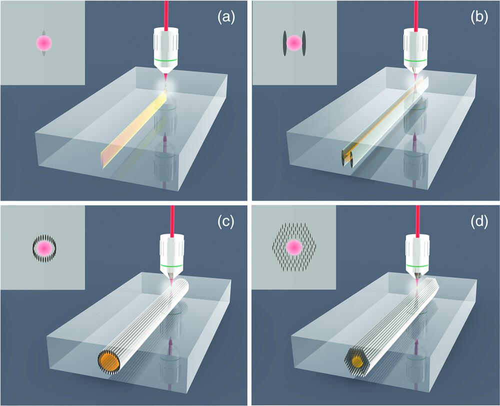
For dielectric crystals, waveguide formation depends on the efficient modification of the refractive index of the bulk. There are two major effects of refractive index changes, i.e., types I and II.63 Type I refers to the laser-induced tracks with positive index changes () that may be due to the slight structural change of lattices. Such variation may be correlated to the breaking of the symmetry of the irradiated lattices.83–85 To form type I modification, low-energy pulses are required. Recent investigation reveals that the type I modification may also be due to the phase transition of the laser-irradiated regions.86,87 Type II refers to laser created filaments in the material, which has negative index changes () caused by localized crystalline lattice expansion in the focal volume.63 The type II modification is typically correlated to highly altered lattices in which partial or complete amorphization occurs. For type I modifications, the track region is able to guide light because it has a higher refractive index than the surroundings, whereas for type II, the track has a lower index and cannot be used as a waveguide; however, the expansion of volume in the focal plane gives rise to compression of vicinity, leading to the refractive index increments in the surrounding of the track.60 With these typical features, several configurations of waveguides have been developed based on types I and II modifications. Figure 1 shows the typical geometries of four basic laser-written waveguides: single-line, double-line, depressed-cladding, and optical-lattice-like structures. For in the track, the single-line can be used to guide light since it naturally constructs a waveguide channel [Fig. 1(a)], and such structures are easy for 3D waveguide fabrication.88,89 However, in crystals, the single-line structure is usually polarization sensitive84,85 and does not possess good thermal stability.32 Another disadvantage is that the waveguide core lattice has been distorted by the laser irradiation and, for crystals, the bulk features are destroyed in the waveguide.90 Based on type I modification, a multiscan technique can be employed for the fabrication of symmetrical waveguides in which several single-line tracks are overlapped transversal to the writing direction.91 Such a design is preferred to support waveguiding accessible to long wavelengths with low-loss propagation owing to a significant increase of the index contrast.89 For , the track region has a low index in comparison with the surrounds, and the vicinal zones have a relatively high index that may serve as guiding regions.92 In practice, to obtain a nearly symmetric waveguide core, the double-line structure is used: the guiding core is located at the region between two parallel tracks [Fig. 1(b)]. The waveguide core is not located at the tracks that have highly altered lattices. This means that the properties of the bulk crystals are well-preserved in the waveguides93,94 in which the laser-induced modifications of the original lattices are negligible.95 In addition, the formed track has excellent thermal stability, enabling applications under high-power conditions.96 There are shortcomings offered by the double-line waveguides, which cannot guide light at longer wavelengths since the dimension of the waveguide core is limited to , and for 3D fabrication it requires a complicated design.97 The depressed-cladding structure is a more flexible solution [Fig. 1(c)]. It is usually in the geometry of circles or rectangles,98 which consists of a number of type II tracks. Since the diameters of cladding waveguides can be artificially determined, they are capable of guiding long-wavelength light, e.g., MIR regime.78,80,99 Nevertheless, for 3D waveguides, it also requires a special design. A special configuration is an “optical-lattice-like” structure,100 which contains a periodically arranged array of tracks [Fig. 1(d)]. Some positions are free of any tracks, e.g., in the center of the structure, which can serve as beam propagation channels. By modulating the geometries of tracks, it is able to achieve beam transformation and shaping.101,102 Generally, the maximum of type I modification is much lower than that of the type II modification induced by femtosecond laser irradiation.32 For instance, the typical index variation of type I waveguides in crystal does not go beyond , whereas this value will increase to (2 to 5) × at directly irradiated tracks for type II-based structures.23,63 For Nd:YAG double-line waveguides, as high as at type II filaments has been determined according to -Raman and -photoluminescence microscopic analysis.92 Most recently, quantitative phase microscopy became a popular method to recover the index contrast of the waveguides from the phase image. In particular, the index change of has been maintained after heating up to 1400°C for a depressed cladding waveguide inscribed in a sapphire crystal that exhibited prior to the annealing process.80Table 1 summarizes the advantages and disadvantages of different configurations in transparent solid materials (crystal, glass, polymer, ceramic, etc).
Sign up for Advanced Photonics TOC. Get the latest issue of Advanced Photonics delivered right to you!Sign up now
Figure 1.Basic geometries of laser writing of waveguides: (a) single-line, (b) double-line, (c) depressed-cladding, and (d) optical-lattice-like configurations. The dark (gray) regions represent the laser-induced tracks.
One could realize the evolution of laser-written tracks from type I to type II via manipulating the laser inscription parameters. For instance, in crystal, with the low-repetition rate of femtosecond laser pulses (25 kHz), the tracks can be changed from type I to type II. Figure 2(a) shows the influence of incident pulse energy on the geometry of tracks at a fixed laser scanning speed. With the increase of pulse energy, the type I region gradually moves down along the direction that the laser propagates and an elongated filamentation with type II modification appears. This can be explained by the competition of self-focusing and plasma defocusing when the peak power is higher than the critical power :32where is the wavelength, is the linear refractive index, and is the nonlinear refractive index. In addition, the laser scanning velocity can be changed to obtain different types of tracks. Figure 2(b) represents the microscope images of laser-written tracks modified from type I to type II, as the scanning speed changes from 6 to , whereas the pulse energy keeps a fixed value of . As the scanning speed decreases, more energy is deposited in the crystal unit volume, leading to more severe lattice distortion or damage, therefore, the slight type I modification will evolve into type II modification. More than that a new phenomenon allowing a significant increase of the refractive index contrast has been recently reported, which is called the effect of femtosecond-laser-induced electronic bandgap shift (FLIBGS).103 When FLIBGS occurs, the absorption edge of the transmission spectrum shifts. At a propagation wavelength near the transparent material electronic resonance, the FLIBGS greatly affects the absorption and thus the refractive index, as predicted by the Kramers–Kronig relations.104 By employing the effect of the FLIBGS, the tracks created by the femtosecond laser exhibit a dispersion of the refractive index, which in ZnSe crystals is the signal of the variation from positive to negative, as shown in Fig. 2(c). However, the FLIBGS effect generally happens in a narrow wavelength window. According to Lapointe et al.,103 at a specific propagating wavelength, the refractive index modification becomes zero (), which means the laser inscription should be invisible, paving the way for new invisibility applications.
Figure 2.Optical microscope images of laser-induced tracks with (a) different pulse energies and (b) scanning velocity in crystal. (c) Different refractive index change profiles from positive to negative, depending on the propagation wavelength in ZnSe crystal. Image (c) is reproduced with permission from Ref. 103, Creative Commons Attribution License (CC-BY).
The track morphology is crucial for laser inscribed waveguides because the track geometry plays an important role in the refractive index changes and stress fields. In addition, track engineering is also essential for nonlinear domain modification and well-defined microstructures.
2.2.1 Effect of writing parameters
For a given laser writing system, the main parameter that determines the localized modification in focal volume is the pulse intensity (or fluence).32 At low pulse intensity but beyond the optical modification threshold, an isotropic refractive index change is achieved,105 whereas a birefringent refractive index change has been obtained at intermediate intensity.106 Higher pulse intensity will lead to empty voids caused by microexplosions,107 depending on the properties of the material. The transverse intensity distribution of the laser beam could be written as108where is the radial distance and is the axial distance from the beam waist. is the variation of the laser beam spot size (the distance from the beam axis where the intensity drops to of the maximum value) and is given by and is the diffraction-limited minimum beam waist radius: where is the Gaussian beam quality factor and NA is the numerical aperture of the focusing objective. The Rayleigh range of the focus within a transparent material having a refractive index is given by
The laser beam focus size at the focal plane is simply given by the and in the transverse and axial directions of the incident beam when neglecting optical aberrations and nonlinear effects. The peak intensities reached at the focal volume of the transparent material are: where is the pulse energy and is the pulse duration. As we can see, the beam waist determines the transversal size of the modifications induced in the dielectrics; together with the scanning velocity, they define the pulses superposition and the total amount of the energy delivered at a focal spot. It also defines the pulses that have enough intensity to promote changes in the material.
Generally, the higher the energy of laser pulses is, the more modified the tracks are.90 In addition, higher-speed scanning creates weaker tracks.23 This is easily understandable because the track geometry is determined by the average energy deposition of the unit volume in the samples. Figure 3(a) shows the laser-induced tracks in a crystal at different energies and scanning rates (the repetition rate of the laser is set at 1 kHz). Similar effects are observed for other crystals. Therefore, the choice of energy and scanning rate for a successful waveguide fabrication is to balance both effects on dielectric materials. The energy of pulses is typical of micro-Joule () or sub-, and the used scanning rate ranges from tens of to tens of mm/s. The polarization of femtosecond laser pulses may also affect the track writing, although in most cases, the effect is negligible. For example, in an optical-lattice-like structure of Nd:YAP crystal,75 as femtosecond laser polarization is perpendicular to the scan direction, the waveguide cores are located in the regions between adjacent tracks, while in the center of the structure in the case of polarization parallel to the scan orientation. Figure 3(b) shows the optical microscope image of the lattice-like structure in a Nd:YAP crystal and the guided modes obtained under different laser polarizations.
The unique characteristics of crystal materials, such as birefringence and optical nonlinearities will affect the track morphology. For example, in , along the crystalline orientation of the axis, the incident laser is split into two beams inside the crystal due to the high birefringence; as a result, two tracks are created at one shot of a single-laser pulse [Fig. 3(c)]. Nevertheless, such behaviors strongly depend on the used laser parameters and the bulk features. In many cases, nonlinear optical effects highly influence the propagation of femtosecond laser pulses in crystals, resulting in the morphology of tracks that are more likely to be an elongated filamentation or structure with multifoci not only a single focus.110,111 It is a very complex dynamic process. As the light propagates through a dielectric, the optical response is described as a macroscopic polarization induced by displacement of bound charges. For the simplified case of a centrosymmetric material that nullified the second order (an all even order), if fourth and higher order nonlinear effects are neglected, the polarization of a centrosymmetric medium can be written as112where is the th order nonlinear susceptibility and is the incident electric field. The refractive index of the material is defined by and (optical Kerr effect) when the linear part dominates over the nonlinear part:32where , , and is the laser intensity. Thereby, a spatially dependent intensity of the Gaussian laser beam modifies the effective refractive index of dielectrics. In most media, the is positive and the refractive index at the center of the beam is higher than in the wings, acting as a positive lens to self-focus the light, as if the femtosecond laser pulse exceeds the , a collapse occurs at a focal point. Additionally, the convex effect induces sufficient intensity to create ionization and other nonlinear effects, forming an electron plasma that acts as a concave lens to defocus the laser beam. The self-focusing comes again provided the intensity is higher than the . Such a spontaneous multiple focusing can be realized in both type I and type II regimes. For example, in crystals, under the high-repetition-rate of femtosecond laser (700 kHz) for type II modification, the altered track consists of three point-like structures at a single shot, which is identified with a periodic distribution of lattice defects.113 Furthermore, the laser-induced grating structure of a period is also implemented. In addition, in the regime of low repetition rate (8 kHz), the multifoci tracks based on type I modification can be demonstrated as the energy increases and the track morphology is determined by the energy of laser pulses.91 Another interesting sample is crystal, where the multiple-focusing spots with different numbers are also realized, depending on the laser-irradiated parameters.109 Using the multiscan technique, researchers have fabricated desired structures to obtain horizontal tracks for waveguide-guiding along with TE polarization, whereas the normal double-line waveguide only supports TM polarization [Fig. 3(d)]. In this design, the layer of the waveguide is composed of a number of modified points, forming a dotted line, and the total length can be controlled by the laser scans. Theoretically, more layers of waveguides can be possibly obtained using this approach.
2.2.3 Beam shaping techniques
During the process of femtosecond laser irradiation, the laser beam is generally fixed and focused at a certain depth beneath the sample surface. The sample is usually mounted on a computer-controlled linear stage to realize an arbitrary shape, and a CCD system is used to monitor the waveguide writing process. The sample can be translated along the beam propagation direction, i.e., longitudinal writing, or orthogonally to, i.e., transverse writing.60 The waveguide formed by longitudinal writing has intrinsic circular symmetry, while it is restricted by the working distance of the objective lens and it has limitations in 3D layouts.114 In contrast, the design flexibility of transverse writing is enormous and allows for the fabrication of 3D structures,23,60 in spite of their asymmetric cross sections.
Over the past decades, beam-engineering techniques have been developed to improve the shape of the laser-written waveguides, such as the double-beam technique,115 adding cylindrical lenses,116 the slit technique,41 using a nondiffractive Bessel beam,117 and using a spatial light modulator (SLM).39Figure 4(a) illustrates the writing process of depressed cladding waveguides utilizing an ellipsoidal focal spot, where a number of tracks are inscribed one by one, thus, resulting in a time-consuming process. Nowadays, SLMs have been used widely in femtosecond laser processing. From the work of Qi et al., the fabrication times have been considerably reduced,41 as shown in Fig. 4(b). The phase mask for writing horizontal lines is presented in Fig. 4(c). Thereby, horizontal tracks can be employed to construct the cladding of waveguides in a crystal that exhibit the polarization-independent guidance42 [Figs. 4(d)–4(f)]. Later in 2019, Zhang et al.118 proposed a single-scan method to fabricate cladding waveguides using 3D engineered focal field [Figs. 4(g)–4(j)]. The longitudinally oriented ring-shaped focal field is composed of 16 discrete spots, allowing for the generation of annular cladding waveguides at a single shot of laser writing, demonstrated in Figs. 4(k)–4(m). Most recently, Sun et al.39 developed a new and efficient multifoci-shaped femtosecond pulsed method to write circular symmetric waveguides with an SLM.
The morphology of tracks is crucial for not only waveguide configuration but also for engineering the crystal properties to achieve modulation of nonlinearity polarization. Especially for type II modification, focused laser pulses will cause highly damaged lattices, where an amorphous volume forms that reduces the nonlinear coefficient. Such a modification can be periodically introduced to realize spatial modulation of the second-order nonlinear coefficient , enabling quasi-phase-matching (QPM) structures,119 also known as nonlinear photonic crystals (NPC).120 Thereby, the researchers have fabricated 3D NPCs by selectively erasing the nonlinear coefficients of a crystal.121 The recently developed 3D NPCs present efficient generations of second-harmonic vortex and Hermite–Gaussian beams, showing the potential for nonlinear beam-shaping devices6 and nonlinear volume holography122,123 in comparison to the two-dimensional (2D) case. Additionally, the huge flexibility of direct laser writing enables complex 3D domain structures,43,120 allowing their monolithic integration with other phase modulators and switches, and improving the performances and functions of on-chip devices. Using the same strategy of domain erasing in a quartz crystal, researchers from Shandong University have realized tunable second harmonic generation (SHG) down to the ultraviolet wavelength.124 In addition, there will be an obvious thermal effect at the high-repetition rate of femtosecond laser pulses, which can be utilized to realize reversed polarization. The group from Australia reported on the similar 3D domain structures in a BCT crystal by femtosecond laser direct writing through the thermoelectric-field poling,125 allowing for precise domain inversion with high resolution. This laser engineering strategy can be extended to other systems of crystals.
Moreover, laser-induced quasi-phase-matching (LiQPM) grating structures inside the waveguide’s core allow efficient frequency conversion, which opens new avenues for advanced all-integrated nonlinear devices. For instance, using femtosecond laser-induced domain inversion in waveguides, a conversion efficiency of 17.45% for frequency doubling of 815 nm has been demonstrated.126 In addition, a depressed cladding waveguide-integrated LiQPM grating scheme has been proposed by Denz et al.127 With the precise and flexible 3D domain engineering, as shown in Figs. 5(a) and 5(b), they have realized broadband and multiwavelength frequency conversions.43 Particularly, the second harmonic vortex can be demonstrated by a helical twisted domain grating into a waveguide, as depicted in Figs. 5(c)–5(e).
The laser-written track is also promising for creating spatially well-defined microstructures in combination with chemical wet etching. In the laser-modified volumes, the femtosecond pulses have driven the crystal network to a predamaged state that shows a larger selective etching than the unperturbed bulk lattices.128 A good sample is the YAG crystal, as shown in Fig. 6(a), where the optical-lattice-like waveguide is fabricated by direct laser writing, and then the sample is immersed into the selected acid (e.g., phosphoric acid).129 As one can see, after some time, the etched portion of the damaged track is filled with air, thus resulting in a larger refractive index change than the unetched region [Figs. 6(b) and 6(c)]. Therefore, the confinement of the light field will be enhanced. In this work, the etched microstructured optical waveguide supports good guidance at the MIR wavelength of [Figs. 6(d) and 6(e)], which is impossible for structure before etching. Actually, early in 2013, Kar et al. produced large microfluidic channels within YAG by selectively wet etching laser-written type I tracks.130 The technique is very interesting and offers an efficient solution to 3D nanolithography of crystals. In 2019, Osellame et al.131 reported on the nanopores with mm-scale length. By implementing auxiliary vertical etching pores to build a 3D-connecting etching architecture, they have achieved 3D nanolithography with a long length. Using this strategy, they have produced subwavelength diffraction gratings and microstructured waveguides in YAG crystals.
Dielectric crystals are important media for optical and photonic applications, which can be roughly cast into a few groups, such as laser crystals, nonlinear optical crystals, and electrooptic crystals.23 Unlike the amorphous substrates, crystalline material entails structures of long-range orders of lattices, offering unique physical properties that are not exhibited in glass, such as even order optical nonlinearities and birefringence.1 There are seven crystal systems to characterize the crystal lattices or structures of different geometries, i.e., cubic, tetragonal, hexagonal, trigonal, orthorhombic, monoclinic, and triclinic. Up to the current date, a wide range of crystals has been used for the fabrication of direct laser-written waveguides; for example, YAG crystal belongs to the cubic, , β, and sapphire crystals belong to the trigonal, and 6H-SiC crystal belongs to the hexagonal crystal family. To some extent, the symmetry of each lattice determines the waveguide properties, such as polarization dependence and propagation loss. Table 2 summarizes the waveguide configurations and guiding properties of typical crystals in different crystal systems. For each lattice family, a brief overview will be given below.
Crystal system
Material
Waveguide configuration
Guiding properties
Ref.
Polarization dependence
Minimum propagation loss (dB/cm)
Cubic crystals
Nd:YAG
Type I (single line)
TE and TM
5@632.8 nm
87
Dual line
TM
0.21@632.8 nm
79
Double cladding
TE and TM
1.3@632.8 nm
132
Optical-lattice like
TE and TM
0.7@1064 nm
100
Cladding + dual line
TE and TM
—
133
Nd:GGG
Dual line
TM
2.0@632.8 nm
134
Depressed cladding
TE and TM
1.7@632.8 nm
135
BGO
Type I (multiscan)
TE and TM
89
Type I (ring shaped)
TE and TM
1.56@1550 nm
136
Dual line
TE and TM
0.5/632.8 nm
137
Depressed cladding
TE and TM
2.1@632.8 nm
137
Tetragonal crystals
Dual line
TE and TM
0.8@632.8 nm
138
Depressed cladding
TE and TM
1.1@632.9 nm
139
Optical-lattice like
—
—
140
Dual line
TM
0.5@1064 nm
141
Depressed cladding
TE and TM
0.7@632.8 nm
142
Hexagonal crystals
6H-SiC
Dual line
TM
0.78@1064 nm
143
Rectangular cladding
TE and TM
1.62@1064 nm
143
Trigonal crystals
Type I (single line)
TM
2.22@1064 nm
144
Type I (multiline)
TM
1.98@632.8 nm
91
Dual line (vertical)
TM
0.6@1064 nm
63
Dual line (horizontal)
TE
3.25@1550 nm
41
Depressed cladding
TE and TM
1.25@1550 nm
118
Optical-lattice like
TE
1.27@1550 nm
145
Ridge configuration
TM
146
Type I (single line)
TM
2.67@632.8 nm
147
Dual line (horizontal)
TE
1.7@632.8 nm
109
Depressed cladding
TE and TM
1.56@1550 nm
148
Rectangular cladding
TE and TM
0.12@1550 nm
149
β-BBO
Depressed cladding
TM
0.19@800 nm
150
Sapphire
Type I
TE and TM
2.3@633 nm
151
Dual line
TM
0.65@798.5 nm
152
Depressed cladding
TE and TM
0.37@2850 nm
80
Optical-lattice like
TE and TM
2.9@1064 nm
153
Orthorhombic crystals
KTP
Type I (multiline)
TM
1.0@980 nm
154
Dual line
TE and TM
0.8@633 nm
155
Depressed cladding
TE and TM
1.7@632.8 nm
156
Optical-lattice like
TE and TM
1.2@632.8 nm
157
Nd:YAP
Depressed cladding
TE and TM
0.15@1064 nm
158
Optical-lattice like
TE and TM
1.11@1064 nm
159
Monoclinic crystals
Depressed cladding
TE and TM
0.6@1064 nm
160
Nd:YCOB
Type I
TM
1,1@1550 nm
85
Depressed cladding
TM and TE
—
161
Nd:GdCOB
Double cladding
TM and TE
0.65@633 nm
162
Nd:KGW
Dual line
TM and TE
2.0@632.8 nm
163
Depressed cladding
TM and TE
1.8@1064 nm
164
Table 2. Summary of latest published works about waveguide configuration and properties of typical crystals in different crystal systems.
For cubic systems, YAG is one of the most well-studied crystals in the direct laser writing of waveguides. For the depressed-cladding and optical-lattice-like waveguides, symmetric guidance for any polarization, i.e., both transverse magnetic (TM) and electric (TE) are supported,100,132 whereas the dual-line geometry only allows TM-polarized guidance,79 which is mainly related to the high symmetry of the cubic system that possesses three fourfold axes of rotation. The cubic-lattice crystals exposed to laser irradiation undergo a severe modification that results in a positive index change in a specific polarization. A similar polarization-dependent guiding behavior is also found in Nd:GGG crystal,134 another typical cubic crystal. Although for the tetragonal system, such as and , only one fourfold axis of rotation is contained, leading to a lower symmetry than that of the cubic system. As a result, the dual-line structure supports guidance along both TE and TM polarizations138,141 but is still of slightly anisotropic guidance. The depressed-cladding waveguides in the tetragonal is guided in an anisotropic way as well, which is different from the cubic YAG crystal. As for the hexagonal system, up to now, only 6H-SiC crystal is employed for laser writing of waveguides.143 Like the cubic system, both TM and TE guidances are determined in rectangular cladding waveguides, whereas only TM guiding mode is supported in dual-line structure. In hexagonal system, there is one six-fold axis of rotation, thus the symmetry is between the cubic and tetragonal systems.
, , β, and sapphire, as the typical crystals belonging to the trigonal system, exhibit unique nonlinearities and birefringence. Therefore, as these crystals are processed under laser writing, there will be some different structural modifications due to the high-order threefold axis of rotation. Various configurations have been inscribed in crystal by femtosecond lasers, such as type I modified single-line and multiline structures, type II modified dual-line waveguides, depressed-cladding, optical-lattice-like, and ride waveguides. Generally, in and crystals, type I and type II waveguides would suffer from serious polarization-dependent guiding, which only permits polarization along the orientation parallel to the laser-induced tracks,91,147 whereas the depressed-cladding waveguide enables isotropic guiding as well as in Ti-sapphire crystal.165 However, for β crystal, only TM-polarized guiding is supported in depressed-cladding waveguides.150 In addition, polarization-dependent guiding also happens in both optical-lattice-like145 and ridge configurations146 in a crystal, which only allows -polarized guidance.
In addition to the crystal system mentioned above there are lower-symmetry crystal families that do not contain a higher-fold axis of rotation, such as orthorhombic system and monoclinic system. In such crystal systems, laser-written waveguides present isotropic guiding behavior. For instance, (KTP) is a typical crystal belonging to the orthorhombic system; the guidance for dual-line,155 depressed-cladding,156 and optical-lattice-like waveguides157 is almost polarization independent. In addition, ,160 Nd:KGW,164 and 166 crystals belong to the monoclinic system, another member of the lower-symmetry family. In these crystals, femtosecond laser-written waveguides mainly focus on the depressed-cladding configuration, which allows symmetric guidance for both TM and TE polarizations due to the poor lattice symmetry. These features imply the unique modification of laser pulses on the crystals with different symmetries.
2.4 Mode Modulation
In recent years, numerous newly developed waveguide geometries that allow mode modulation and guiding polarization engineering have been demonstrated, benefiting from the rapid and direct prototyping of femtosecond laser writing.
For type I modification, the multiscan technique offers a flexible manner to tailor the mode profiles by controlling the number and separation of laser-induced tracks91 [Fig. 7(a)]. In addition, by arranging the laser-modified tracks into an annular ring, the ring-shaped mode profiles in BGO crystal have also been obtained,136 as shown in Fig. 7(b). In particular, such a design allows for polarization-independent guiding, which is different from single- and multiline type I waveguides that only support one special polarized guiding. In addition, the rings can be inscribed in the desired diameter to meet the practical applications. Theoretically, one could realize mode modulation with arbitrary geometries by proper design and arrangement of the laser-induced tracks.
As for type II modification, one can fabricate a series of dotted lines along the horizontal direction via multiscan, modulating the modal profiles along the TE polarization owing to the changed stress field distribution,167 as shown in Fig. 7(c). At recent reports in SiC crystal, the mode modulation of waveguides has also been achieved by controlling the morphology of laser-induced tracks.143 In addition, femtosecond laser-written waveguide arrays based on type II modification can implement mode modulation via the effect of evanescent coupling. For example, the one-dimensional planar waveguide laser arrays in Nd:YAG crystals support flexible discrete diffraction by adjusting the coupling condition.170 Zhang et al.37 reported the 2D waveguide arrays in crystal, where the output mode profiles can be modulated as the pump beam goes into the array at different positions.
Beyond the above reports, some designs based on the depressed-cladding structures also enable mode modulation. Sun et al. proposed an “ear-like” waveguide structure with extra tracks at the sides of cladding, which is an evolved scheme of double-line and depressed-cladding waveguides that was first reported by Okhrimchuk et al.171 Such a design is intended to further enhance the optical confinement of the light field. Therefore, more symmetric mode profiles and lower propagation losses are preferred compared with the normal cladding waveguides,168 as shown in Fig. 7(d). Another interesting sample is the double-cladding waveguide [Fig. 7(e)], which is composed of two concentric tubular shapes with different diameters.172 One of the advantages is that the outer cladding could enhance the coupling efficiency of the pump beam and inner cladding permits an output beam with low-order modes, i.e., generating an integrated single-mode laser system.169 Moreover, using a third-cladding structure, Wu et al.132 demonstrated annular ring waveguide lasers, promising for complex integrated pump sources to alleviate thermal lensing.
3 Designs for Laser-Written 3D Crystalline Photonic Devices
New emerging photonic devices with 3D configurations have attracted considerable attention. Femtosecond laser writing, as the most efficient technique for true 3D microfabrication, allows an arbitrary geometry in almost any transparent substrate. Although various laser-written 3D structures have been successfully fabricated in glass,34,173–177 the complexity of lattice and anisotropies make it much difficult to manipulate in crystals. Special designs are, therefore, required by varying the writing parameters and track geometries. In this section, we will overview the recent reports on waveguide-based 3D photonic structures, such as -branches, beam steering elements, ring-shaped transformers, polarizers, tapered structures, and directional couplers.
3.1 Y-Branches
As the basic 3D components, a branch-based splitter allows for dividing the single-input beam into several output beams in different dimensions. For example, the 3D waveguide beam splitters () based on type-I modification have been realized in 88 and BGO crystals,89 whereas the polarization-dependent properties are very different for the two crystalline waveguides. The only supports light propagation along particular orientations, whereas wave guidance in BGO is isotropic for any transverse polarization. As for type-II modification, -branches work well in a relatively simple way for 2D structures, as reported in diamond178 and YAG crystals.97 However, in the 3D case, disadvantages are emerging due to the unbalanced guiding properties and additional architecture required to connect separate channels. Moreover, the geometry of depressed cladding supports wave-guiding along any polarization, and for 3D fabrication it also requires a complicated design. The buried -junctions based on circular and rectangular depressed-cladding geometries have been proposed in YAG179,180 and Ti:sapphire crystals,181 as shown in Figs. 8(a)–8(e), which produce smooth transitions and preserve modal profiles. Furthermore, Ajates et al. reported the novel 3D beam splitting based on depressed-cladding architecture in crystals [Fig. 8(f)], realizing the desired 3D guiding path.182 Although the TM-polarized modes have higher losses than that of TE, the 3D structures work well in the near-infrared band. It is possible to implement any arbitrary 3D photonic circuit in crystalline materials based on circular cladding waveguides.
3.2 Photonic-Lattice-Like Structures for 3D Microfabrication
Additional branched boundaries are essential for beam splitters in Sec. 3.1; as a result, the fabrication processing is usually time-consuming. To this end, the family for 3D microfabrication is designed, known as an “optical-lattice-like” photonic structure, which contains a number of periodic tracks with geometry defects. A typical structure has a track layer of hexagonal layout, where the light field is confined at enclosed track-free regions. Particularly, better guiding confinement is followed at multilayers rather than single layer. Tailored beam steering in the 3D manner, such as beam splitting or ring-shaped transformation,100 can be realized by directly introducing additional defect tracks at certain positions. These defect lines served as beam blocks or confiners that smoothly reshape the guiding profiles during the propagation; therefore, no additional losses are introduced.102 Based on this strategy, 3D beam steering of ring-shaped transformation has been successfully inscribed in YAG crystals,100 as shown in Figs. 9(a) and 9(b). In addition, highly compact 3D beam splitters () have been implemented in many platforms, such as ,145,157 Nd:YAG, and Ti-sapphire crystals153 [Figs. 9(c)–9(e)]. By carefully considering the crystalline properties, more advanced applications, such as nonlinear frequency conversion183 and miniature laser sources have been demonstrated.101 Such 3D designs could efficiently improve the integration of complex photonic circuits. Considering the huge differences in the characteristics of crystals, however, each type requires a different 3D inscription and feasible optimization scheme.
In photonic integrated circuits (PICs), the undesirable effect of polarization dependence limits the practical applications of polarization-division multiplexed systems. Hence, polarization diversity devices including polarizers, polarization beam splitters (PBSs), and polarization rotators attract researchers’ interest. Femtosecond laser writing provides an on-demand fabrication method for polarization photonic devices. Recently, a new structure of polarizer has been employed to engineer the guiding polarization in crystals,184 as depicted in Figs. 10(a) and 10(b), which is composed of three parts: a rectangular-shaped channel, a beam splitter acting as the connection element, and two output channels. In such a structure, the output will be well-separated into TE and TM polarized light as the polarized light or hybrid light of TE plus TM modes enters the waveguide [Fig. 10(c)]. The polarization extinction ratio and insertion loss can be comparable with that of fused-silica-based PBS. In addition, a 3D polarizer in a cross-shaped geometry has been produced in crystal,167 consisting of a square cladding waveguide and four vertically oriented double lines [Figs. 10(d) and 10(e)]. This 3D configuration enables specific polarized-light output at different waveguide arrays, i.e., the TM or TE-polarized light can be controllably coupled into vertical or horizontal waveguide arrays, respectively.
Tapered waveguide structures, like the tapered optical fibers, have different circular radii of input and output arms. In 2020, Romero et al.185 proposed a 3D tapered waveguide by smoothly decreasing the separation between the tracks that consisted of the depressed-cladding waveguide, as shown in Fig. 11(a). This approach enables the desired reduction of the input/output radius, allowing highly multimodal coupling into single-mode waveguides, as depicted in Fig. 11(b). It is particularly interesting for waveguide laser systems, which reaches a higher coupling efficiency of the pump beam and enhanced intensity of the output power compared to a straight waveguide with the same radius. In addition, such a 3D design offers an efficient manner for modal formatting or light concentration [Fig. 11(c)]. Another promising scheme is the 3D waveguide array,37 which has a potential application in 3D photonic devices, such as photonic lanterns. Figure 11(d) illustrates the prototype of 3D waveguide arrays in Nd:YAG crystals,186 which are composed of seven adjacent hexagonal cladding structures at the input face and have each waveguide separated radially from the center at a certain distance at the output face, as shown in Fig. 11(e). This design shows a good wave guiding for both the visible and near-infrared bands. The directional coupler is the basic building block for integrated classical and quantum photonic circuits.45Figure 12(a) presents the 3D design of a directional coupler based on a depressed-cladding waveguide in a crystal187 in which several cladding tracks are removed to form the coupling region [Fig. 12(b)]. The top and cross-section view microscope images are shown in Figs. 12(c) and 12(d). Single-mode guidance with an output splitting ratio of 19:40:41 at 810 nm was demonstrated in this work [Fig. 12(e)], indicating the potential applications in quantum storage devices. By integrating embedded 3D electrodes on both sides of the coupling region of the buried directional coupler in a crystal,118 as shown in Fig. 12(f), the efficiency of electro-optic modulation was finely improved [Fig. 12(g)].
In recent years, direct femtosecond laser writing of dielectric crystals enables various waveguiding structures, offering an ideal platform for a broad range of photonic applications by considering the bulk properties of the materials used. In this section, selected advances in recent applications of laser-written crystalline waveguides are overviewed.
4.1 Waveguide Lasers
Benefitting from the high optical confinement, femtosecond laser-written waveguides provide efficient miniaturized laser sources that cover the spectral range from visible to MIR (530 nm to ) with many advantages, such as reduced lasing thresholds, enhanced slope efficiencies, compact size, nondiffraction beams, and multifunctional integration.7 Up to now, some notable improvements have been achieved, depending on the active ions and the mechanisms for lasing. Table 3 summarizes the reported results for waveguide lasers emitting at different wavelengths based on various cavity designs fabricated in femtosecond laser writing.
Wavelength band
Gain media
Working wavelength (nm)
Cavity configuration
Operation regime
Laser performance
Ref.
Lasing threshold (mW)
Max. output power (mW)
Slope efficiency
Visible
531
Cladding
CW
5
0.1
—
161
532
Dual line
CW
—
0.032
—
188
634.5
Dual line
CW
190
28.1
8%
189
525.3
Dual line
CW
1088
36
190
644
516
1065
37%
724.9
885
504
25%
604
Rhombic cladding
CW
360
25
5.6%
191
720
243
12
2.0%
Ti : sapphire
700 to 870
Dual line
CW
84
143
23.5%
192
798.5
Dual line
CWML (21.25 GHz)
1160.1
87.48
—
152
Near-infrared
1013.9 and 1027.9
Cladding
CW and -switched
152.2
26.6
10%
193
Yb : YAG
1030
-curved dual line
CW
141
1 W
79%
194
-branch dual line
CW
271
2.29 W
52%
97
Dual line
-switched
102
5.6 W
74%
195
Dual line
QML (2 GHz)
1800
322
11.3%
196
Double cladding
CW
401.7
45.8
38%
172
Yb : KLuW
1040
Surface cladding
-switched
491
680
61%
197
Nd : YAG
1064
Annular ring shaped
CW
191
84
20%
132
Ear-like cladding
CW and -switched
10
327
34.4%
168
Cladding
-switched
287
102.3
11.9%
198
QML (8.8 GHz)
74
127
26%
199
1061.58 and 1064.18
Cladding
CWML (9.8 GHz)
—
530
—
200
1064
-branch cladding
CW
231
172
22.4%
180
1 × 2 splitters
CW
90
333
34%
101
1 × 4 splitters
90
217
22%
Ring shaped
CW and -switched
148
224
22%
100
1064
Cladding
CW
10.3 W
3.4 W
36%
139
-switched
57.4
275
37%
201
QML (6.5 GHz)
65
424
56%
202
CWML (6.5 GHz)
19.3
259
30.6%
203
Double cladding
-switched
59
397
46%
169
Optical-lattice like
-switched
—
85
20%
140
Nd : YAP
1064 and 1079
Cladding
CW
243
199.8
33.4%
158
-curved cladding
QML (7.9 GHz)
196
77
14.1
159
-curved optical-lattice like
228
57
10.69
1072 and 1079
Optical-lattice like
CW
384.5
101.3
30.9
75
1063.6
Dual line
CW
52
256
70%
141
1064.5
Cladding
CW and -switched
178
570
68%
142
Nd : GGG
1061
Dual line
CW
29
11
25%
134
1063
Cladding
CW
270
209
44.4%
135
1066.4
Dual line
CW
98
30
14%
204
Nd : KGW
1065
Dual line
CW
141
33
52.3%
163
1067
Cladding
CW
120
198.5
39.4%
164
MIR
1847.4
Surface cladding
CW
52
171.1
37.8%
205
1846.8
-switched
500
150
34.6%
1849.6
Cladding
CW
45
247
48.7%
206
1844.8
-switched
—
24.9
9.3%
1847
Optical-lattice like
CW
21
46
9.9%
207
1841 to 1848
-branch cladding
CW
280
460
40.6%
208
Tm : YAG
1943.5
Cladding
QML (7.8 GHz)
665
6.5
2%
209
2055
Cladding
CW
180
212
67.3%
210
2080
Surface cladding
CW
120
132
38.9%
211
Ho : YAG
2091
Cladding
QML (5.9 GHz)
—
170
6.8%
212
2096
CW
100
1775
16%
213
Cr : ZnS
2333
Cladding
CW
450
101
20%
214
Cr : ZnSe
2522
Cladding
CW
—
5200
41%
215
Fe : ZnSe
4070
Cladding
CW
—
995
58%
Table 3. Summary of reported results for waveguide lasers emitting at different wavelengths based on various laser-cavity designs.
Laser emission at visible wavelengths mainly relies on -doped gain media, such as , , and crystals. For instance, using well-established dual-line structure, a green waveguide laser operating at 525.3 nm was first demonstrated in crystals.190 Since then, based on the rhombic cladding geometry, orange and deep red laser oscillations at 604 and 720 nm were produced in crystal.191 Moreover, laser-written active dual-line waveguides in Ti:sapphire have offered tunable laser operating from 700 to 870 nm.192 In addition, with the same dual-line configuration in Ti:sapphire, Grivas et al.152 reported a femtosecond continuous-wave mode-locked (CWML) laser emitting at 790 nm. The generated waveguide laser was operated at pulses of 41.4 fs with a fundamental repetition rate up to 21.25 GHz.
Near-infrared spectral range is the most common laser emission band, which is gained by writing an active waveguide into well-known - and -doped crystals. Beyond a normal straight laser cavity, it is also possible to achieve efficient optical feedback for lasing oscillation in curved and branched cavity geometry owing to an enhanced optical gain of a waveguide laser. For example, in femtosecond laser-written 3D structures, compact waveguide lasers at have been proposed in different functionalities, such as -curved,159,194-branches,97,180,208,216 and beam splitting,101 ring-shaped beam transformation,100,132 and optical-lattice-like lasing75 [Figs. 13(a)–13(e)]. Laser performance in these reports is comparable to that of straight waveguides, suggesting a superior flexibility for prototyping laser sources using femtosecond laser writing. By further integrating a suitable absorber, passively -switched lasing has been realized. For example, using a high gain Yb:YAG channel waveguide, an efficient -switched laser has shown a slope efficiency of 74% with an average power up to 5.6 W in a single-pass optical pumping without any reflective mirrors.195 Most recently, mode-locked waveguide lasers operating at multi-gigahertz (GHz) regimes have attracted increasing interest. For instance, 6.5 GHz -switched mode-locked (QML) lasers have been demonstrated in a femtosecond laser-written cladding waveguide using 2D materials as the saturable absorber.202 Another recent sample is Nd:YAP crystal : 31.6-GHz QML lasers have been demonstrated in an -curved waveguide,159 as shown in Fig. 13(f). In particular, both single- and dual-wavelength (1064 and 1079 nm) lasing can be achieved by tuning the pump polarization [Figs. 13(g) and 13(h)].
Recently, MIR () waveguide lasers, typically obtained from - and -doped materials, have attracted much attention from researchers. For a gain medium of , efficient waveguide lasers at operating both in the CW and -switched regimes have been reported by Kifle et al. in various laser-written waveguide structures, such as -branch splitters,208 surface cladding,205 buried circular cladding,166,206 and photonic-lattice-like cladding prototypes.207 In addition, their group has demonstrated a low-loss () waveguide laser in a crystal at with a slope efficiency of 64.4%.211 Also, in the multi-GHz operation regime, 5.9- and 7.8-GHz QML waveguide lasers at have been successfully achieved in 212 and Tm : YAG,209 respectively. Cr:ZnS is another host medium for MIR laser generation. Based on the cladding channel waveguide, an efficient 2333-nm waveguide laser with an output power of 101 mW has been reported by Macdonald et al.214 Moreover, waveguides written in Fe:ZnSe crystal have shown a slope efficiency of 58%, offering a working wavelength up to 4070 nm.215
4.2 Frequency Converters
Frequency conversion displayed in femtosecond laser-written waveguides coming from second and higher-order nonlinearities offers an efficient manner to access special wavelengths. Similar to waveguide lasers, frequency converters in waveguide structures provide enhanced conversion efficiencies compared to bulk material, as a result of strong optical confinement and good overlap between the fundamental and nonlinear polarization waves over the whole interaction length. Femtosecond laser-written waveguides allow for nonlinear optical conversion, mainly SHG, at a wavelength range between and 790 nm.
One of the most well-studied nonlinear crystals is , since the work of Burghoff et al.217 in 2007, which enabled efficient frequency doubling of 1064 nm with a conversion efficiency of 49% in laser-written dual-line waveguides. In 2021, using the regime of birefringent phase matching (BPM), waveguide geometries of multiline, vertical dual line, and depressed cladding have also been reported in crystals for SHG of 1064 nm,218 whereas BPM is difficult to realize in some crystals with weak birefringence. In recent years, LiQPM grating structures have attracted a particular interest in frequency doubling, beginning from the first proof in 2013 reported by Thomas et al.119 though with a poor conversion efficiency. Later in 2015, an increased conversion efficiency of 5.72% was reported by Kroesen et al., which introduced QPM grating structure inside a depressed-cladding waveguide.127 In 2020, a waveguide-integrated 3D QPM grating scheme was proposed, as shown in Fig. 14(a), thus multiwavelength SHGs of 1065.3, 1064, 1061.6, and 1060.5 nm radiation have been demonstrated43 [Fig. 14(b)]. Using this technique, Wei et al.121 produced 3D NPC in crystals, as well as realizing an SHG of 829 nm with an enhanced second-harmonic power compared with the on-engineered area. Figure 14(c) illustrates the setup of the SHG process using LiQPM structures in quartz crystal, and a deep-ultraviolet generation of 177.3 nm has been achieved with a high efficiency of 1.07‰124 [Fig. 14(d)]. In addition, based on a type I single-line waveguide, the green-up conversion at 550 and 528 nm and NIR emission at 1550 nm have been reported in crystals.144 Moreover, spontaneous parametric down-conversion from 780 to 1560 nm has also been demonstrated in laser-written multiline waveguides of PPLN crystal, giving access to photon entanglement in quantum technologies.49
Frequency doubling down to ultraviolet bands has also attracted much attention. cladding waveguide is a good sample, and a violet SHG at 400 nm has been realized.219 crystal is another promising material owing to its shorter cut-off wavelength () and high optical damage threshold. In 2019, a second harmonic power up to 8.5 W was realized in laser-written circular-cladding waveguides under a CW pump at 1050 nm in a periodically poled (PPMgSLT) crystal.220Figure 14(e) depicts the schematic plot of femtosecond laser direct writing cladding waveguides in fan-out PPMgSLT crystals, corresponding to different poling periods. Temperature-tuned SHG for different QPM periods has been demonstrated in Fig. 14(f) with a comparable normalized conversion efficiency of .148 Later in 2020, a tunable violet SHG over the range of 396 to 401 nm was demonstrated by varying the QPM condition in fan-out PPMgSLT crystals,221 evincing efficient frequency converters based on femtosecond laser-written waveguides.
(KTP) is another excellent nonlinear platform for frequency conversion. In 2007, the laser-written multiline waveguide based on type I modification permitted SHG down to 400 nm in periodically (PPKTP) crystals.154 Lately, a further improvement of conversion efficiency () has been proposed in type II dual-line waveguides in Rb-doped PPKTP crystals.222 In particular, due to the true 3D micromachining of femtosecond laser writing, optical lattice-like beam splitters in KTP crystals have enabled SHG of 1064 nm by BPM.157 In addition, the optical-lattice-like microstructures offer an efficient manner for beam mode controlling, providing a simple way to realize single-mode frequency doubling at 532 nm with a comparable conversion efficiency.183Table 4 summarizes the latest results for frequency converters based on femtosecond laser-written waveguides.
Crystal
Waveguide configuration
Laser regime
(nm)
(nm)
SHG configuration
()
Norm. efficiency ()
Ref.
BBO
Cladding
CW
800
400
BPM
1.05 mW
0.98%
219
PPKTP
Type I (multiscan)
CW
800
400
QPM
0.02%
154
PPSLT
Cladding
CW
800
396 to 401 (tunable)
QPM
0.37 mW
0.39%
221
PPKTP
Dual line
CW
943.18
471.59
QPM
76 mW
4.6%
222
Cladding
Pulsed
1030
515
BPM
—
—
223
Type I (multiline)
Pulsed
1064
532
BPM
12.45 W (peak)
0.27%
218
Dual line
Pulsed
1064
532
BPM
4.95 W (peak)
0.14%
Cladding
Pulsed
1064
532
BPM
40.40 mW (peak)
0.87%
Cladding
Pulsed
1064
532
LiQPM
25.1 W (peak)
0.0637%
127
Cladding
Pulsed
1065.3, 1064, 1061.6, and 1060.5
532.65, 532, 530.8, and 530.25
LiQPM
1.33 W (peak)
0.64% ()
43
PPMgSLT
Cladding
CW
1064
532
QPM
0.74%
224
Cladding
CW
1050
525
QPM
8.5 W
0.16%
220
Cladding
CW
1064
532
QPM
14.87 mW
3.55%
148
Cladding
Pulsed
1064
532
QPM
153 W (peak)
54.3% ()
Optical-lattice like (1 × 4 splitters)
CW
1064
532
BPM
0.65 mW
1.5%
157
Optical-lattice like (straight)
CW
1064
532
BPM
0.67 mW
0.87%
Hybrid optical-lattice
CW
1064
532
BPM
0.8 mW
1.1%
121
Table 4. Summary of latest results for frequency converters in femtosecond laser-written waveguides.
To date, femtosecond laser direct writing has played an important role in integrated quantum information processing,225,226 such as integrated sources of entangled photons,49 high-dimensional transmission of quantum twisted light states,47 2D quantum walk,46 and the rotated polarization directional coupler.45 Quantum memories (QMs) are essential components in large-scale quantum networks, especially in quantum repeaters. Rare-earth ion-doped crystals are promising candidates of integrated QMs due to their large bandwidth, high multimode capacity, and high storage fidelity.227 Two approaches have been employed to manufacture integrated QMs in rare-earth ion-doped crystals, such as Ti-indiffusion in 15 and focused-ion-beam milling.228 Nevertheless, the storage time and efficiencies in these two systems are significantly reduced. In recent years, femtosecond laser direct writing has allowed channel waveguides with improved capabilities, where the active ions are directly coupled to the light, rather than via evanescent coupling.52,225,229 As a result, spin-wave storage with an extended lifetime, which enables long-term storage and on-demand read-out, has been achieved in waveguide-integrated QMs.50,51,53,230 A great amount of effort has been devoted to this topic, mainly focused on the geometry of type I, type II, and ridge waveguides.
The first proof of QMs based on laser-written dual-line waveguides was reported in crystals, where the interaction with the active ions is increased by a factor of 6 compared to bulk, and demonstrated a spin-wave optical memory,229 as shown in Figs. 15(a)–15(d). Later in 2020, using the type II waveguides in crystals, on-demand light storage was demonstrated via the spin-wave atomic frequency comb (AFC) and the storage fidelity was quantitatively characterized for the first time.50 Compared to type II waveguides, the fabrication of type I waveguides in crystalline substrates is still a very challenging task, as it requires a very narrow writing window. In 2018, Seri et al.52 produced high-quality type I waveguides in crystals, demonstrating efficient storage times 100 times longer than previous demonstrations [Figs. 15(e)–15(g)]. In the next year, their group reported more than 130 individual storage modes in laser-written type I waveguides in crystals, among the temporal, spectral, and spatial domains, demonstrating the capability of both time and frequency multiplexing single photon.53 Such high multimodality will be necessary to realize an efficient quantum repeater scheme.
Considering that the channel waveguides (type I and type II) are fabricated at a depth beneath the crystal surface, ridge waveguide-based QMs are easily integrated with other on-chip devices, allowing for constructing large-scale quantum networks. In 2020, a laser-written ridge waveguide was successfully fabricated in an crystal, in which the properties of the ions were well-preserved.230 The spin-wave AFC storage was implemented, confirming high-interference visibility [Figs. 16(a)–16(d)]. In 2021, their group achieved a better fabrication parameter, realizing 40% end-to-end device efficiency, while the typical coupling efficiency is 10% in waveguide memory. Combined with on-chip electrodes, a high storage fidelity of and on-demand storage of time-bin qubits were demonstrated,51 far beyond that value of the classical measure-and-prepare strategy.
Thin-film lithium-niobate-on-insulator (LNOI) has attracted significant interest in the field of PIC for its favorable low-loss limit and electro-optic coefficients.17,18,231 With the recent revolution in fabrication techniques of on-chip photonics, great progress has been sparked in producing ultrahigh performance building blocks, such as waveguides16,232 and microcavities,233 for scalable and high-density LNOI PICs. In 2015, Lin et al.234 first reported on the fabrication of high- microresonators by femtosecond laser direct writing, followed by focused ion beam milling. In 2018, their group proposed an efficient LNOI fabrication technique termed photolithography-assisted chemo-mechanical etching (PLACE).235Figures 17(a)–17(e) schematically illustrate the process of PLACE, including mainly five steps. Notably, femtosecond laser micromachining is used to pattern the Cr thin film into a waveguide- or circular disk-shaped mask with the advantages of high scanning speed and high quality. The key in this step is to carefully choose a peak intensity of the femtosecond laser, in which the Cr film can be completely removed without damaging the underneath LNOI, since the ablation threshold of LNOI is significantly higher than that of the metal Cr.233 In addition, chemomechanical polishing (CMP) is employed to selectively etch smooth sidewalls capable of low scattering loss. Using this technique, a 10-cm-long LNOI waveguide with an ultralow loss of 232 [Figs. 17(f)–17(h)] and an LNOI microresonator with an ultrahigh factor of by improving the surface roughness of 233 [Fig. 17(i)] have been demonstrated. In addition, by adding a layer of film on the waveguides, a single-mode LNOI waveguide with a propagation loss of at 1550 nm has also been discussed.236 Based on these ultralow-loss waveguides, Wang et al.237 demonstrated the fabrication of LNOI beam splitters and Mach–Zehnder interferometers. Later in 2020, Zhou et al.236 successfully designed and fabricated optical true delay lines on the LNOI chip, realizing a relative time delay of 2.285 ns. Various waveguides with lengths from to have been fabricated with losses below , providing the large-scale on-chip integration of numerous unit microdevices.
To date, some active components, such as on-chip microlasers and amplifiers, have also played an important role in the monolithic integration of PICs. In 2021, Wang et al.238 demonstrated a tunable microring laser on -doped LNOI, enabling a low threshold of . In the same year, by integrating the microelectrodes, an electro-optically tunable microring laser has been achieved on an LNOI platform on which the laser wavelength can be tuned with an electro-optic coefficient of .239 Specifically, their group provided an alternative pumping manner, using an undoped LNOI waveguide directly bonded above the -doped microring, rather than the tapered fibers. In addition, Zhou et al.240 proposed an on-chip waveguide amplifier on -doped LNOI, which allows a net gain of 18 dB for a length of 3.6 cm emitting of 1530 nm, indicating an efficient broadband amplification.
5 Summary and Perspectives
Femtosecond laser inscribed crystalline waveguides play increasingly significant roles in modern photonic circuits, offering an attractive platform for multifunctional integrated optical applications. The unique 3D microfabrication of femtosecond lasers is currently driving the success of new devices and functionalities, such as quantum and on-chip photonics. Recent progress and achievements in this research field are briefly overviewed, whereas a few challenges and potential topics remain to be further investigated.
First, the underlying mechanism of different refractive index modifications induced by femtosecond lasers is not entirely understood, which strongly depends on the parameters of the laser processing system and the physical properties of crystals. For example, an interesting phase transformation from YAG to YAP crystal is observed by Okhrimchuk et al.86 under direct laser writing, relating to rapid quenching after overheated crystal melting. Future investigation towards the mechanisms of refractive index modification and the phase-change transitions is planned. Second, a severe limitation of femtosecond laser inscription is related to the relatively lower refractive index contrast than that of bulk, usually on the magnitude of in crystals. Thus the miniaturization of femtosecond laser-processed photonic devices and many applications are limited. Further work will focus on the formation of waveguides with an enhanced photoinduced refractive index contrast while preserving the morphology and uniformity of laser-induced modifications. Third, waveguide-integrated photonic devices have a significant interest in large-scale on-chip circuits, thus the waveguide performances, including propagation loss, bending radii, and coupling efficiencies with other optical components, need to be further improved via optimizing design and fabrication. Benefitting from the 3D capability of femtosecond laser writing, more complex structures are expected to improve the integration density for multifunctional devices in crystals, such as lantern waveguides,174 high-channel interposers,176 and helical waveguide arrays175 that have been achieved in glass. Fourth, some femtosecond laser micromachined on-chip LNOI devices as mentioned in Sec. 4.4 are opening an avenue for scalable integrated applications. Notably, the outstanding nonlinear properties of LNOI compared with silicon on insulator will be very attractive for future PICs. Therefore, the performance of LNOI requires further investigation by carefully designed domain structures for enhancing nonlinear conversion efficiency, whereas femtosecond laser-engineered domain modification is an efficient manner. Considering a relatively large nonlinear coefficient (), LT-on-insulator (LTOI) is another fascinating alternative for on-chip photonics who possesses a higher optical damage threshold () and a greater UV transparency (0.28 to ), whereas there is little research in LTOI devices and their nonlinear characterization.241 Fifth, laser-written waveguides may receive wider applications in the field of quantum photonics. Most recently, using a single-mode waveguide and a doughnut-shaped waveguide fabricated by femtosecond laser direct writing, Chen et al.48 demonstrated the vector vortex beam emitter carrying spin and orbital angular momentum mode inside a photonic chip, allowing for high-dimensional quantum information processing. Further optimizations concern the research of indistinguishable vortex photonic states and on-chip quantum interference. In addition, laser-written waveguides play an important role in single-photon sources, and QMs based on rare-earth doped waveguides, promising potential applications at the visible wavelength band. Large memory arrays and matrices in one crystal can be expected for massively multiplexed QMs in the near future.
In summary, recent advances of femtosecond laser-written waveguides in crystalline materials are overviewed. First, this review presents an introduction to the modification induced by femtosecond laser processing of dielectric crystals, including the fundamentals, control of laser-induced tracks, beam shaping techniques, waveguide geometries, and mode modulation. Track morphology engineering is crucial for not only tailoring the properties of the waveguide but also for the fabrication of novel photonic structures, such as 3D NPCs, 3D domain grating structures, nanopores, and microstructured optical waveguides. Then progress in 3D laser-written photonic devices is discussed, including 3D beam-splitters, tapered waveguides, 3D waveguide arrays, and 3D directional couplers. Last but not least, the selected applications, such as waveguide lasers, frequency converters, QMs, and on-chip devices, have been reviewed in detail. Future challenges and potential topics that could be realized in laser-written waveguides have also been proposed. Overall, it can be concluded that femtosecond laser micromachined waveguides in crystals are still rapidly developing and expected to present the possibility for truly 3D-integrated on-chip photonics in the near future.
Lingqi Li received her PhD from Shandong University, Jinan, China, in 2021. She is an assistant professor at the College of Physics Science of Qingdao University. From 2019 to 2020, she was a joint PhD student for a research at the Max Born Institute for Nonlinear Optics and Short-Pulse Spectroscopy. Her current research interests include femtosecond laser micro- and nanofabrication, waveguide lasers, nonlinear optics, interaction of intense femtosecond laser pulses with materials, and femtosecond pulse characterization.
Weijin Kong received his PhD from Shanghai Institute of Optics and Fine Mechanics, Chinese Academy of Sciences, in 2006. He is currently a professor at the College of Physics Science, Qingdao University, China. His research interests include micro-nano optics, waveguide laser, diffraction optics, and thin film optics.
Feng Chen received his PhD from Shandong University in 2002. He is currently a distinguished professor at the School of Physics of Shandong University. From 2003 to 2005, he was at the Clausthal University of Technology, Clausthal-Zellerfeld, Germany, as an Alexander von Humboldt research fellow. In 2006, he became a professor at Shandong University. His research interests include material modifications by ultrafast lasers and ion beams, optical waveguides, 2D materials, plasmonics, nonlinear optics, and lasers. He is a fellow of the Institute of Physics, OPTICA (formerly OSA), and SPIE, and a director board member of Chinese Physical Society. He serves as the executive editor-in-chief of Chinese Optics Letters, associate editor of Optical Engineering, and an editorial board member of Scientific Reports.
References
[1] D. N. Nikogosyan. Nonlinear Optical Crystals: A Complete Survey(2005).
[2] A. A. Kaminskii. Laser Crystals: Their Physics and Properties(2013).
[3] P. Ferraro et al. Ferroelectric Crystals for Photonic Applications: Including Nanoscale Fabrication and Characterization Techniques(2009).
[113] A. Rodenas et al. Confocal Raman imaging of optical waveguides in LiNbO3 fabricated by ultrafast high-repetition rate laser-writing. Opt. Express, 16, 13979-13989(2008).