• Advanced Photonics
  • Vol. 2, Issue 1, 014001 (2020)
Xueqian Zhang1, Quan Xu1、*, Lingbo Xia1, Yanfeng Li1, Jianqiang Gu1, Zhen Tian1, Chunmei Ouyang1, Jiaguang Han1、*, and Weili Zhang2、*
Author Affiliations
  • 1Tianjin University and the Key Laboratory of Optoelectronics Information and Technology (Ministry of Education), Center for Terahertz Waves and College of Precision Instrument and Optoelectronics Engineering, Tianjin, China
  • 2Oklahoma State University, School of Electrical and Computer Engineering, Stillwater, Oklahoma, United States
  • show less
    DOI: 10.1117/1.AP.2.1.014001 Cite this Article Set citation alerts
    Xueqian Zhang, Quan Xu, Lingbo Xia, Yanfeng Li, Jianqiang Gu, Zhen Tian, Chunmei Ouyang, Jiaguang Han, Weili Zhang. Terahertz surface plasmonic waves: a review[J]. Advanced Photonics, 2020, 2(1): 014001 Copy Citation Text show less
    Simulation results of various THz SPWs using a commercial eigenmode solver. All the boundaries along the x direction are set as periodic with p=100 μm, and the field distribution of real-Ez is simulated for a phase shift of π/2. (a) Simulated THz SPWs on a bare metal surface. (b) Simulated THz SPWs on a cylindrical metal wire with a radius of 100 μm and the electric field along the y-z plane. (c) Simulated THz SPWs on a metal surface coated with a 20-μm-thick dielectric film (ε=2.96), and the top-right inset illustrates zoomed-in electric fields. (d) Simulated THz SPWs on a PGL and the electric field in the y-z plane. Here, the PGL with a 10-μm width and 1-μm thickness is patterned on a 100-μm-thick dielectric substrate (ε=2.96). (e) Simulated THz SSPPs. Here, the textured structure in each period has a height of 70 μm and width of 50 μm. (f) Simulated dispersion relations of various THz SPWs in the first Brillouin zone, and the top-left inset illustrates a zoom-in of the dispersion relations.
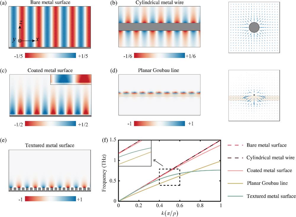
    Fig. 1. Simulation results of various THz SPWs using a commercial eigenmode solver. All the boundaries along the x direction are set as periodic with p=100  μm, and the field distribution of real-Ez is simulated for a phase shift of π/2. (a) Simulated THz SPWs on a bare metal surface. (b) Simulated THz SPWs on a cylindrical metal wire with a radius of 100  μm and the electric field along the y-z plane. (c) Simulated THz SPWs on a metal surface coated with a 20-μm-thick dielectric film (ε=2.96), and the top-right inset illustrates zoomed-in electric fields. (d) Simulated THz SPWs on a PGL and the electric field in the y-z plane. Here, the PGL with a 10-μm width and 1-μm thickness is patterned on a 100-μm-thick dielectric substrate (ε=2.96). (e) Simulated THz SSPPs. Here, the textured structure in each period has a height of 70  μm and width of 50  μm. (f) Simulated dispersion relations of various THz SPWs in the first Brillouin zone, and the top-left inset illustrates a zoom-in of the dispersion relations.
    Excitation and detection of THz SPWs. (a) Schematic of experimental setup used for exciting SPWs on a gold film of 300-nm thickness covered with a dielectric film, where the incoming THz beam is focused on the aperture h1.47" target="_self" style="display: inline;">47 (b) Cross-section detail of the experimental setup using parallel-plate waveguide to couple THz SPWs from free-space THz waves.70" target="_self" style="display: inline;">70 (c) Schematic of the Otto prism setup for coupling and decoupling THz SSPPs.53" target="_self" style="display: inline;">53 (d) Illustration of the experimental setup to couple normally incident free-space THz waves to SPWs using reciprocal lattice vector G=kSPW.99" target="_self" style="display: inline;">99 (e) The top-left inset schematically shows the transmitter chip, the top-right inset schematically shows the receiver antenna and the output face of the copper wire, and the bottom inset schematically shows the cross section of the transmitter chip, the copper wire, and the detection chip, respectively.67" target="_self" style="display: inline;">67 (f) Schematic diagram of the PGL waveguide (w=5 μm) fabricated on a quartz substrate with integrated 70 μm×70 μm photoconductive switch regions.100" target="_self" style="display: inline;">100 Figure reprinted with permission: (a) Ref. 47, © 2004 by the American Physical Society (APS); (b) Ref. 70, © 2009 by the Optical Society of America (OSA); (c) Ref. 53, © 2013 by Wiley-VCH; (d) Ref. 99, © 2018 by OSA; (e) Ref. 67, © 2005 by the American Institute of Physics (AIP); and (f) Ref. 100, © 2009 by AIP.
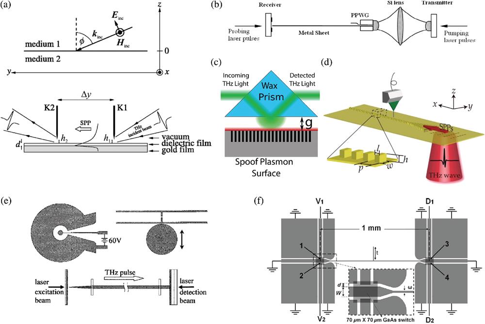
    Fig. 2. Excitation and detection of THz SPWs. (a) Schematic of experimental setup used for exciting SPWs on a gold film of 300-nm thickness covered with a dielectric film, where the incoming THz beam is focused on the aperture h1.47 (b) Cross-section detail of the experimental setup using parallel-plate waveguide to couple THz SPWs from free-space THz waves.70 (c) Schematic of the Otto prism setup for coupling and decoupling THz SSPPs.53 (d) Illustration of the experimental setup to couple normally incident free-space THz waves to SPWs using reciprocal lattice vector G=kSPW.99 (e) The top-left inset schematically shows the transmitter chip, the top-right inset schematically shows the receiver antenna and the output face of the copper wire, and the bottom inset schematically shows the cross section of the transmitter chip, the copper wire, and the detection chip, respectively.67 (f) Schematic diagram of the PGL waveguide (w=5  μm) fabricated on a quartz substrate with integrated 70  μm×70  μm photoconductive switch regions.100 Figure reprinted with permission: (a) Ref. 47, © 2004 by the American Physical Society (APS); (b) Ref. 70, © 2009 by the Optical Society of America (OSA); (c) Ref. 53, © 2013 by Wiley-VCH; (d) Ref. 99, © 2018 by OSA; (e) Ref. 67, © 2005 by the American Institute of Physics (AIP); and (f) Ref. 100, © 2009 by AIP.
    Direct mapping systems for THz SPPs. (a) Schematic diagram of the experimental setup for imaging the THz-SPWs. The generated THz-SPWs propagate along the x-axis in the vicinity of a foil. A quarter wave plate, a Wollaston prism, and a charge-coupled device camera are used for differential detection. The ZnTe crystal is mounted on a 1-D positioning stage and auto-scanned along the x-axis.116" target="_self" style="display: inline;">116 (b) Schematic diagram of the near-field scanning THz microscopy system. The red and blue beams represent the laser and THz radiations, respectively. A linear polarizer and a quarter-wave plate are used to change the polarization state of the THz wave, which illuminates the sample from the substrate side. The THz probe, which detects the near-field electric component of Ez, is fixed on a two-dimensional translation stage.118" target="_self" style="display: inline;">118 Figures reprinted with permission: (a) Ref. 116 © 2014 by OSA, and (b) Ref. 118, © 2015 by AIP.
    Fig. 3. Direct mapping systems for THz SPPs. (a) Schematic diagram of the experimental setup for imaging the THz-SPWs. The generated THz-SPWs propagate along the x-axis in the vicinity of a foil. A quarter wave plate, a Wollaston prism, and a charge-coupled device camera are used for differential detection. The ZnTe crystal is mounted on a 1-D positioning stage and auto-scanned along the x-axis.116 (b) Schematic diagram of the near-field scanning THz microscopy system. The red and blue beams represent the laser and THz radiations, respectively. A linear polarizer and a quarter-wave plate are used to change the polarization state of the THz wave, which illuminates the sample from the substrate side. The THz probe, which detects the near-field electric component of Ez, is fixed on a two-dimensional translation stage.118 Figures reprinted with permission: (a) Ref. 116 © 2014 by OSA, and (b) Ref. 118, © 2015 by AIP.
    Controlling excitation of THz SPWs by metasurfaces. Schematic views of (a) single SR and (b) paired SRs, respectively. (c) Photograph of part of the metasurface and (d) the transverse SPW distributions in the xy-plane under the LCP, RCP, and linearly polarized THz incidences, respectively. The intensity of the SPWs excited by the LCP incidence is approximately three times stronger than that of RCP incidence, which verified the circular polarization analysis function of this metasurface.128" target="_self" style="display: inline;">128 (e) Microscope images of (left) fabricated metasurface, and the measured Ez-field-amplitude distributions of THz SPWs under normal incidences of the (middle) LCP and (right) RCP polarizations, respectively.129" target="_self" style="display: inline;">129 (f) Optical images of fabricated metasurface, and (g1, g3) the measured electric field and (g2, g4) phase distributions, respectively.130" target="_self" style="display: inline;">130 (h) Schematic view of a ring-shaped hologram, and (i) the measured V- and N-shaped THz SPW intensity profiles (|Ez|2) that are generated from a polarization-controlled SPW hologram.131" target="_self" style="display: inline;">131 (j) Microscope image of a part of the fabricated metasurface and (k) the measured Ez-field-amplitude distribution under normal incidence of an x-polarized wave.132" target="_self" style="display: inline;">132 (l) Scanning electron micrograph image of a fabricated metasurface unit, and (m) the measured Ez-field-amplitude distributions in the case of the x-polarized, y-polarized, LCP, and RCP incidences, respectively, left to right.133" target="_self" style="display: inline;">133 Figures reprinted with permission: (c), (d) Ref. 128, © 2015 by AIP; (e) Ref. 129, © 2015 by Wiley-VCH; (f), (g) Ref. 130, © 2018 by Wiley-VCH; (h), (i) Ref. 131, © 2017 by Wiley-VCH; (j), (k) Ref. 132, © 2016 by the American Association for the Advancement of Science; and (l), (m) Ref. 133, © 2017 by OSA.
    Fig. 4. Controlling excitation of THz SPWs by metasurfaces. Schematic views of (a) single SR and (b) paired SRs, respectively. (c) Photograph of part of the metasurface and (d) the transverse SPW distributions in the xy-plane under the LCP, RCP, and linearly polarized THz incidences, respectively. The intensity of the SPWs excited by the LCP incidence is approximately three times stronger than that of RCP incidence, which verified the circular polarization analysis function of this metasurface.128 (e) Microscope images of (left) fabricated metasurface, and the measured Ez-field-amplitude distributions of THz SPWs under normal incidences of the (middle) LCP and (right) RCP polarizations, respectively.129 (f) Optical images of fabricated metasurface, and (g1, g3) the measured electric field and (g2, g4) phase distributions, respectively.130 (h) Schematic view of a ring-shaped hologram, and (i) the measured V- and N-shaped THz SPW intensity profiles (|Ez|2) that are generated from a polarization-controlled SPW hologram.131 (j) Microscope image of a part of the fabricated metasurface and (k) the measured Ez-field-amplitude distribution under normal incidence of an x-polarized wave.132 (l) Scanning electron micrograph image of a fabricated metasurface unit, and (m) the measured Ez-field-amplitude distributions in the case of the x-polarized, y-polarized, LCP, and RCP incidences, respectively, left to right.133 Figures reprinted with permission: (c), (d) Ref. 128, © 2015 by AIP; (e) Ref. 129, © 2015 by Wiley-VCH; (f), (g) Ref. 130, © 2018 by Wiley-VCH; (h), (i) Ref. 131, © 2017 by Wiley-VCH; (j), (k) Ref. 132, © 2016 by the American Association for the Advancement of Science; and (l), (m) Ref. 133, © 2017 by OSA.
    Applications of THz SPWs. (a) The left-top photo is the scanning electron image of a straight waveguide, and the left-bottom is the schematic of an S-bend and a Y-splitter. The three figures on the right side are the corresponding measured THz SSPP |Ez|2 distributions.99" target="_self" style="display: inline;">99 (b) Simulated field concentration via adiabatic dispersion variation, and (c) simulated superfocusing on a corrugated cone with the radius reduced from 100 to 10 μm along a 2-mm length, where the magnitude of the electric field on a logarithmic scale spans two orders of magnitude.153" target="_self" style="display: inline;">153 (d) Schematic of the interaction process of the incident THz wave with the meta-hole structure, and (e) the experimental RCP and LCP transmissions at 0.78 THz, respectively.159" target="_self" style="display: inline;">159 (f) Scanning electron microscopic image of the Si array of elliptical through holes, and (g) measured frequency-dependent THz transmission through the array of perpendicular orientation under various laser excitations ranging from 0 to 111 mW.89" target="_self" style="display: inline;">89 (h) Concept view of sensing using SSPPs and the sensing results for different objects.53" target="_self" style="display: inline;">53 Figures reprinted with permission: (a) Ref. 99, © 2018 by OSA; (b), (c) Ref. 153, © 2006 by APS; (d), (e) Ref. 159, © 2018 by Wiley-VCH; (f), (g) Ref. 89, © 2007 by APS; and (h) Ref. 53, © 2013 by Wiley-VCH.
    Fig. 5. Applications of THz SPWs. (a) The left-top photo is the scanning electron image of a straight waveguide, and the left-bottom is the schematic of an S-bend and a Y-splitter. The three figures on the right side are the corresponding measured THz SSPP |Ez|2 distributions.99 (b) Simulated field concentration via adiabatic dispersion variation, and (c) simulated superfocusing on a corrugated cone with the radius reduced from 100 to 10  μm along a 2-mm length, where the magnitude of the electric field on a logarithmic scale spans two orders of magnitude.153 (d) Schematic of the interaction process of the incident THz wave with the meta-hole structure, and (e) the experimental RCP and LCP transmissions at 0.78 THz, respectively.159 (f) Scanning electron microscopic image of the Si array of elliptical through holes, and (g) measured frequency-dependent THz transmission through the array of perpendicular orientation under various laser excitations ranging from 0 to 111 mW.89 (h) Concept view of sensing using SSPPs and the sensing results for different objects.53 Figures reprinted with permission: (a) Ref. 99, © 2018 by OSA; (b), (c) Ref. 153, © 2006 by APS; (d), (e) Ref. 159, © 2018 by Wiley-VCH; (f), (g) Ref. 89, © 2007 by APS; and (h) Ref. 53, © 2013 by Wiley-VCH.
    Xueqian Zhang, Quan Xu, Lingbo Xia, Yanfeng Li, Jianqiang Gu, Zhen Tian, Chunmei Ouyang, Jiaguang Han, Weili Zhang. Terahertz surface plasmonic waves: a review[J]. Advanced Photonics, 2020, 2(1): 014001
    Download Citation