1Tianjin University and the Key Laboratory of Optoelectronics Information and Technology (Ministry of Education), Center for Terahertz Waves and College of Precision Instrument and Optoelectronics Engineering, Tianjin, China
2Oklahoma State University, School of Electrical and Computer Engineering, Stillwater, Oklahoma, United States
Terahertz science and technology promise many cutting-edge applications. Terahertz surface plasmonic waves that propagate at metal–dielectric interfaces deliver a potentially effective way to realize integrated terahertz devices and systems. Previous concerns regarding terahertz surface plasmonic waves have been based on their highly delocalized feature. However, recent advances in plasmonics indicate that the confinement of terahertz surface plasmonic waves, as well as their propagating behaviors, can be engineered by designing the surface environments, shapes, structures, materials, etc., enabling a unique and fascinating regime of plasmonic waves. Together with the essential spectral property of terahertz radiation, as well as the increasingly developed materials, microfabrication, and time-domain spectroscopy technologies, devices and systems based on terahertz surface plasmonic waves may pave the way toward highly integrated platforms for multifunctional operation, implementation, and processing of terahertz waves in both fundamental science and practical applications. We present a review on terahertz surface plasmonic waves on various types of supports in a sequence of properties, excitation and detection, and applications. The current research trend and outlook of possible research directions for terahertz surface plasmonic waves are also outlined.
Terahertz (THz, ) waves, generally defined in the frequency range of 0.1 to 10 THz, lie between the microwave and infrared frequencies in the electromagnetic spectrum.1–3 With unique spectral properties, THz radiation promises many cutting-edge applications,4–6 including molecular exploration, identification and sensing, nondestructive evaluation, high-resolution radar and imaging, and homeland security. In particular, THz technology is of great potential in developing next-generation, ultrahigh-speed communications, owing to its broad frequency band and capability in carrying ultralarge amounts of information.7,8 To promote THz science and technology into real applications, it is highly desirable to realize THz sources, detectors, and devices of high efficiency, quality, and performance.
Traditional THz devices, such as parabolic mirrors, lenses, waveplates, and polarizers, are commonly large in volume, leading to bulky THz systems. Meanwhile, a challenge with such systems is direct detection of a small quantity of analytes, due to the limited interaction length. Recent advances in metasurfaces have opened an efficient route to realizing compact devices with desired functionalities.9–12 The resonance nature of the composite unit cells in metasurfaces greatly enhances their interaction with THz waves. Furthermore, the resonance can be freely engineered in unit cell design, allowing efficient manipulation of the local phase, amplitude, and polarization on a subwavelength scale, thus controlling the overall spectral response and wavefront of the devices. Typical THz metasurface devices include filters,13,14 sensors,15–18 absorbers,19–21 modulators,22–26 polarization controllers,27,28 flat lenses,29–32 special beam generators,33,34 holograms,29,35–37 cloaks,38,39 etc. Though much more compact than their traditional counterparts, these metadevices have little effect in reducing the size of the THz propagation path in the systems. One promising way to solve this problem is excitation of THz surface plasmonic waves (SPWs), whose confined fields enable efficient interaction with analytes in sensing and modulation applications. More importantly, SPWs allow chip-scale THz manipulation, propagation, and processing simultaneously.
SPWs, arising from collective oscillations of the electrons, are a special type of electromagnetic wave, propagating at the interface between a metal and a dielectric.40,41 Replacing free-space propagating electromagnetic waves with SPWs can greatly reduce the device and system design from three dimensions to two dimensions. The interaction between photons and electrons makes the wave vector of the SPWs greater than that of the free-space waves, resulting in a confined field, which is exponentially decaying from the interface. Owing to such a property, the field of SPWs at the interface is greatly enhanced. While propagating along the surface, SPWs interact strongly with materials with a large interaction length, making them promising in surface sensing and nonlinear applications.42,43 Meanwhile, SPWs propagate also along line-guided metallic structures, such as stripes, grooves, and gaps, which endows SPWs with great potentials in integrated plasmonic components for signal waveguiding and processing, toward communications and photonic circuits.44,45 However, such promising properties and potentials are regarded as only effective for SPWs in the optical range, i.e., surface plasmon polaritons (SPPs). In the spectroscopically and technologically important THz regime, however, as metals commonly behave as perfect electric conductors, THz SPWs cannot be well confined at the interface, making THz SPWs less focused in the above-mentioned applications.
Sign up for Advanced Photonics TOC. Get the latest issue of Advanced Photonics delivered right to you!Sign up now
In fact, recent studies have shown that THz SPWs can also be well confined on bare metal wires,46 dielectric-film-coated metal surfaces and wires,47,48 planar Goubau lines (PGLs),49 and textured metal surfaces,50 as well as doped semiconductor, superconductor, and graphene surfaces.51,52 By further bridging with the unique THz spectral properties, SPW-based THz devices and systems can be quite feasible in applications beyond those in the optical regime, such as chip-scale spectral identification, sensing and monitoring, next-generation ultrahigh speed modulation and communications.53–55 At the same time, THz SPWs share similar wave properties with their optics counterparts, and thus the excitation and propagation control methods can be well transformed between the two regimes. In terms of design and characterization, related optical devices usually require state-of-the-art scanning near-field optical microscopy and nanofabrication, making investigations very complex and expensive to implement. However, with the development of semiconductor technology and THz time-domain spectroscopy, characterization of THz SPWs and fabrication of THz SPW-based devices become straightforward. Thus, THz frequencies become a promising platform to explore functionalities, potential properties, and applications of SPWs in a wide spectral range.
In this article, we review SPWs in the THz regime. In Sec. 2, we briefly introduce the propagation properties of THz SPWs on various supports, including bare and coated metal surfaces and wires, PGLs, and textured metal surfaces, as well as doped semiconductor, superconductor, and graphene surfaces. In Sec. 3, we review the excitation and detection techniques of THz SPWs and introduce a direct near-field mapping method for THz SPWs. In Sec. 4, we highlight recent progress in manipulating propagation of THz SPWs upon excitation using metasurfaces. In Sec. 5, several real applications of THz SPWs are presented, including on-chip spectroscopy, waveguiding control, super focusing, beam collimating, extra-ordinary transmission (EOT), active control, and sensing. Finally, in Sec. 6, we present a summary and an outlook on possible future research directions and potential applications of THz SPWs.
2 SPWs in the THz Regime
Early studies on SPWs can be traced back to Sommerfeld’s and Zenneck’s theoretical work on surface waves on metal wires and surfaces in the radio frequency band in the 1900s.56,57 After decades of investigation, the concept and theory were established in 1968 by Kretschmann and Raether.58 Recent research interest in SPWs arose from the observation of EOT in subwavelength metallic hole-arrays in 1998.59 SPW-induced EOT was soon demonstrated in the THz regime.60–62 It has been found that THz SPWs exist at various types of supports with different propagation behaviors. In this section, we divide these SPWs by their propagation conditions and discuss their dispersion relations.
2.1 THz SPWs on Bare Metal Surfaces
Planar bare metal surfaces are the most simple and common support for SPWs. The key properties of the SPWs lie in the dispersion relation, which can be calculated by solving Maxwell’s equations at the metal surface:41where is the wave vector of the SPWs with being its wavelength; is the angular frequency, is the velocity of light in free space, and and are the dielectric constants of the semi-infinite dielectric and metal, respectively. The boundary condition determines that SPWs only exist in the TM mode. In addition to , there are mainly three characteristic parameters of the SPWs, which can be obtained from Eq. (1): (i) the intensity penetration depth that determines the confinement, where is the vacuum wave vector; (ii) the intensity propagation length that determines how long the intensity of the SPWs can maintain; and (iii) dispersion of the phase velocity and group velocity that determine the time-domain propagation behavior. In the THz regime, since is very large (), the wave vector of the THz SPWs is nearly equal to that of the free-space THz wave to an accuracy of 1 part in , resulting in a highly delocalized homogeneous field of the SPWs with a large penetration depth and negligible dispersion.41 The corresponding electric field of the SPWs nearly only contains components perpendicular to the metal surface. Such SPWs are also known as Zenneck waves.57,63 The delocalized property makes it hard to distinguish between the free-space THz waves and the guided THz SPWs, as well as hard to excite a pure THz SPW. The theoretical propagation length of THz SPWs is extremely long. For instance, the field propagation length at 0.4 THz is about 385 m at an aluminum–air interface, and the corresponding field penetration depth is 21.5 cm. In real cases, due to surface roughness and power transfer to the momentum-matched free-space wave, the actual field of THz SPWs is weakly confined at the interface for several millimeters, and the field propagation length also becomes as short as tens of centimeters, as experimentally demonstrated by Jeon and Grischkowsky.64
Besides planar metal surfaces, THz SPWs in the TM mode also exist on bare metal wires for waveguiding applications.46,65–67 Such SPWs are also known as Sommerfeld waves.56,63 Due to the symmetry of the wires, the field of the SPWs is radially polarized. Though the dispersion relation is nearly identical to that on planar bare metal surfaces, the field confinement is much improved. Wang and Mittleman46 experimentally measured such THz SPWs on steel wires with a diameter of 0.9 mm, revealing good propagation features of negligible group velocity dispersion and low loss (). The penetration depth was on the order of several millimeters. Such features were also experimentally demonstrated by Jeon et al.67 on a copper wire with a 0.52-mm diameter, where a radial decay of the SPW field from the surface was reported with being the radius of the wire and being the radial distance from the center of the wire, which means that the penetration depth gets smaller as the diameter decreases. Later, Wang and Mittleman reported a study on the phase velocity dispersion of SPWs on metal wires with different diameters.66 Distinct phase velocity dispersion behavior was found on planar bare metal surfaces, where the phase velocity deviated increasingly from in a nonlinear way as the THz frequency decreased. Such unique behavior became enhanced when the diameter of the wire was decreased.66
2.2 THz SPWs on Coated Metal Surfaces
To overcome the confinement problems of THz SPWs on planar bare metal surfaces, many effective approaches were explored. One simple way was to coat a thin dielectric film at the metal interface, which was demonstrated in the infrared regime earlier.68,69 In the THz regime, such behavior also exists. Saxler et al.47 experimentally observed such an effect and found that a larger film thickness would lead to stronger field confinement, and meanwhile, higher frequencies had better field confinement than lower frequencies. Later, Gong et al.70 proposed a detailed experimental study on the propagation behavior of THz SPWs on coated aluminum surfaces and revealed similar field confinement behavior. They also proposed an effective waveguide theory to explain such a confinement. Due to the highly conductive nature of metals, such a configuration can be seen as a grounded dielectric film waveguide, which effectively acts as a dielectric slab waveguide whose thickness is doubled. When the film thickness is in the deep subwavelength regime, only the mode exists, which corresponds to the THz SPWs. The field confinement can be increased by an order of magnitude compared to that on bare metal surfaces. They demonstrated that a thin film of a thickness of 1/50 wavelength can make the SPW field collapse by 200 times compared to that on bare metal surfaces.70 Changing the film thickness will cause a change of both the phase velocity dispersion and the group velocity dispersion of the SPWs, as well as the field confinement, making it very promising in sensing applications. This can be attributed to the frequency-dependent penetration depth on coated metal surfaces, even though the dielectric coatings themselves do not have any dispersion. Different frequency components have different interaction cross sections with the coated film, resulting in a frequency-dependent effective index. Meanwhile, if the dielectric coating is lossy, the propagation length will decrease. Similar behavior has also been found in THz SPWs on coated metal wires, where the guided THz pulses get strongly chirped during propagation.48 Apart from sensing, it has been experimentally demonstrated that the dielectric coating within a certain thickness range can protect THz SPWs from outside intrusions in real cases, thus increasing the propagation length.71
2.3 THz SPWs on PGLs
PGLs are a type of planar transmission line, that is, planar single-line-shape structures patterned on a substrate.63,72 Unlike other transmission lines, such as microstrip lines and coplanar transmission lines,73–76 where the supported modes are more like parallel waveguide modes, the surface mode on PGLs has a mode pattern similar to that of Sommerfeld waves on metal wires, namely, a quasi-TM SPW mode. Thus, the basic properties of SPWs on PGLs follow a trend similar to SPWs on metal wires. The polarization of the SPW field is symmetric with respect to the central plane of the PGLs.49,77 However, they are more compact and designable owing to their flat nature. The width of the PGLs can only be several micrometers, and thus the field confinement is greatly enhanced. For a -wide PGL with a thickness on a glass substrate, the simulated overall field confinement is from 0.14 to 0.22 THz, as reported by Treizebré et al.77 Such a good confinement property also makes the PGLs have a larger propagation loss but a smaller bending loss. For a gold PGL with a width and a thickness on a crystalline quartz substrate, the measured propagation loss was at 0.14 THz and at 0.22 THz, as demonstrated by the same group.49 Due to the existence of the substrate, the propagation of the SPWs is greatly influenced by the substrate modes, which can be simply excited by the propagating SPWs, thus increasing the propagation loss even though the substrate is lossless.78,79 Therefore, it is better to make PGLs on substrates with an effective permittivity close to that of air. Russel et al.54 demonstrated that a thinner substrate could support a broader band for THz SPW propagation. Similar to coated metal wires, the SPW pulses on PGLs also suffer from strong dispersion.
2.4 THz SPWs on Textured Metal Surfaces
Another effective way to increase the confinement of THz SPWs is to design subwavelength textured structures on metal surfaces, which can tightly confine the surface mode, as discussed by Mills and Maradudin.80 Pendry et al.41,81 theoretically generalized and extended such a concept even for perfect conductor surfaces, allowing engineering the dispersion of the supported surface mode at nearly arbitrarily lower frequencies. The supported surface mode well mimics the characteristics of the optical SPPs without having to introduce new materials and is called spoof SPPs (SSPPs). For a semi-infinite perfect electric conductor with periodic square-shape holes in a square lattice, whose side length and period are both on the deep subwavelength scale and whose hole thickness is infinite, the corresponding dispersion relation of the SSPPs is given as81where is the effective plasma frequency of the textured structure. Clearly, is freely engineerable by the geometry of the structure and is a real number larger than the vacuum wave vector, indicating a well-confined field and also an infinite propagation length. shows a dramatic frequency-dependent feature and deviates more and more from as the frequency increases, indicating both decreased phase velocity and group velocity at higher frequencies. A smaller side length results in a smaller and weaker confinement, which reverts to the case of planar bare metal surfaces when the side length approaches zero. A similar trend also occurs when the thickness of the hole decreases. If the structure has anisotropic features, such as rectangular holes, the dispersions of the SSPPs along the length and width directions will also present an anisotropic feature. In practical cases where real metals have a finite conductivity, the propagation length will reduce accordingly due to the loss of the metals.82 Such an engineerable characteristic of the textured surface endows a powerful platform for manipulating SPWs in the THz regime, namely, THz SSPPs. Williams et al. took a measurement of the THz SSPP confinement on a structured copper surface. The measured intensity penetration depth was on the order of wavelength, and the estimated intensity propagation length was about 5 cm around the band edge.50 Aside from hole-type structures in metals, pillar-type structures, grooves, and planar structures could also support THz SSPPs.53,83,84 In particular, the planar metal structures have been demonstrated to be able to support SSPPs in the TE mode.85
2.5 THz SPWs on Doped Semiconductor, Superconductor, and Graphene Surfaces
As mentioned at the beginning of this section, the highly delocalized behavior of THz SPWs at metal surfaces is due to their large permittivity, which is related to the large values of determined by the free electron density. Therefore, one direct method to get better confined THz SPWs is to use supports with a smaller at THz frequencies, such as doped semiconductors.41 Rivas et al.51,86 demonstrated the existence of THz SPWs on a doped silicon grating. However, such behavior is accompanied by a larger field penetration into the semiconductor, resulting in larger absorption due to the electron collision effect. One of the advantages of THz SPWs on semiconductor surfaces is the active control of the doping level by temperature, optical pump, magnetic field, etc., which is promising in switching and tuning applications.87–91
Savel’ev et al.92 predicted the existence of terahertz surface waves in layered superconductors below the Josephson plasma frequency , and such waves are called surface Josephson plasma waves (SJPWs). In a semi-infinite sample, SJPWs can propagate along the interface between an external dielectric and a layered superconductor. Similar to optical SPPs in normal metals, the resonance excitation of SJPWs is accompanied by Wood anomalies in the reflection and transmission of THz waves through layered superconductors. Due to resonant excitation of SJPWs, the reflectivity of the incident wave depends sharply on its frequency and incident angle, which is quite useful for filtering and detecting THz and sub-THz radiation using layered superconductors.93 Further details on the basic mechanisms and potential applications of SJPWs are discussed by Savel’ev et al.94
Recent demonstrations revealed that THz SPWs are also supported on graphene, whose effective plasma frequency is lower than that of metals as well. Gan et al.52 presented a theoretical study on TM SPWs on monolayer graphene sheets and separated parallel pair of graphene monolayers in the mid-infrared and THz regimes (0.8 to ), respectively, where the fields can both be well confined. They found that monolayer graphene sandwiched by two lossless dielectrics could only support SPWs in the antisymmetric mode, where the tangential magnetic field switched sign across the graphene. A higher permittivity of the surrounding dielectric will result in a better field confinement. For the parallel graphene pair, they found that it supported both symmetric and antisymmetric modes, depending on whether the magnetic field changed sign across the gap of the graphene pair, and that the dispersion could be tuned both by the separation of the graphene pair and by uneven control of their chemical potential. In both cases, increasing the chemical potential would decrease the confinement. Similar to metal wires and PGLs, graphene ribbons could also serve as THz SPW waveguides, as theoretically studied by Nikitin et al.95 It was found that the graphene ribbons could support SPWs in both waveguide mode and edge mode, whose dispersions are different, and could be tuned by changing the ribbon width and external dielectric environment. Aside from TM SPWs, it was also reported that graphene could support TE SPWs in the THz regime.96
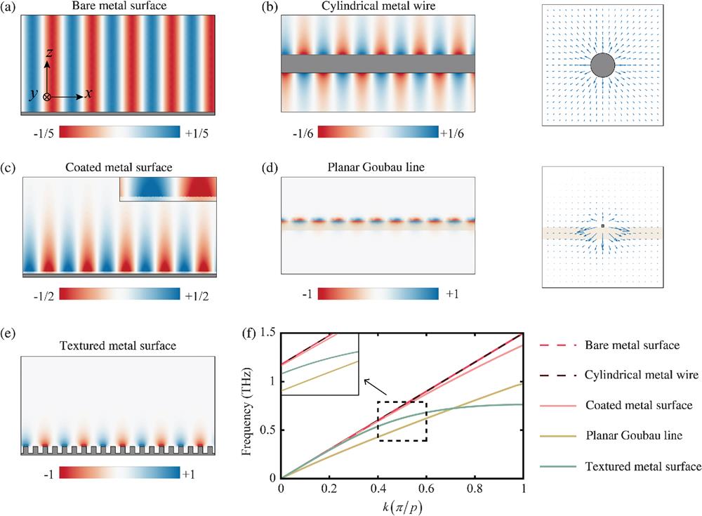
To gain a clear understanding of the dispersion relation of the above-mentioned SPWs on different supports, we have carried out several simulations based on perfect conductors in the THz regime. Figures 1(a)–1(e) show the field distributions of the supported SPWs for clear and schematic comparisons, and the corresponding simulated dispersion relations are given in Fig. 1(f). Here, we mainly focus on THz SPWs on metal-based supports; the results of dispersion relations for doped semiconductors, superconductors, and graphene are not presented.
Figure 1.Simulation results of various THz SPWs using a commercial eigenmode solver. All the boundaries along the direction are set as periodic with , and the field distribution of real- is simulated for a phase shift of . (a) Simulated THz SPWs on a bare metal surface. (b) Simulated THz SPWs on a cylindrical metal wire with a radius of and the electric field along the plane. (c) Simulated THz SPWs on a metal surface coated with a -thick dielectric film (), and the top-right inset illustrates zoomed-in electric fields. (d) Simulated THz SPWs on a PGL and the electric field in the plane. Here, the PGL with a width and thickness is patterned on a -thick dielectric substrate (). (e) Simulated THz SSPPs. Here, the textured structure in each period has a height of and width of . (f) Simulated dispersion relations of various THz SPWs in the first Brillouin zone, and the top-left inset illustrates a zoom-in of the dispersion relations.
To explore the propagation property of THz SPWs and the performance of SPW-based THz devices and systems, it is crucial to find effective ways to excite and detect THz SPWs, so as to enable real applications. In this section, we review several methods on the excitation and detection of THz SPWs.
3.1 Excitation of THz SPWs
Due to the lack of direct SPW sources in the THz regime, it is required to couple the free-space THz wave into SPWs. Similar to the optical regime, the key to excite THz SPWs is also based on the momentum match. In this section, we review traditional methods on excitation of THz SPWs. The recently emerged simultaneous excitation and control of THz SPWs using metasurfaces with the wavefront control ability will be discussed in Sec. 4.
3.1.1 Edge scattering
By illuminating the free-space THz wave onto a sharp edge above the SPW supports with a subwavelength distance, the scatted wave contains components with a broad range of wave vectors, part of which can match those of the SPWs in a broad frequency range. Since SPWs are in the TM mode, in addition to momentum match, the mode match should also be considered. The polarization of the incident wave should contain electric components in the propagation plane of the SPWs formed by the direction of and the surface normal. In the work of THz SPWs on coated gold surfaces, Saxler et al.47 applied a razor blade placed above the surface. By obliquely focusing an in-plane-polarized THz wave onto the edge, broadband THz SPWs were excited, as shown in Fig. 2(a). Such a method also applies to supports with larger SP wave vectors. In the work of SSPPs on a textured copper surface made of periodic square holes, Williams et al.50 also applied the same method to excite broadband THz SSPPs. Besides the above vertical configuration of the edge to the surface, edges fabricated on the supports or on the edges of the supports can also be used to excite THz SPWs. In the work on heavily boron-doped silicon pillar waveguides, Kumar et al.97 fabricated a coupling groove at the input side. Under normal incidence of the THz wave polarized perpendicularly to the groove, SSPPs were coupled into the waveguide. Knyazev et al.98 applied the edge on a coated metal surface to excite THz SPWs by Bessel beams with different orbital angular momentum. An exotic excitation behavior was revealed, where the excitation efficiency of the SPWs depends on the direction of the azimuthal component of the incident-radiation Poynting vector. In addition to planar surfaces, such a method could also be applied to excite SPWs on metal wires. In the work of Wang and Mittleman46 on bare steel wires, a second metal wire was placed perpendicularly to the first metal wire with a gap aperture, forming an intersection structure. The horizontally polarized THz wave was focused onto the aperture, where the input THz radiation was partially scattered to the SPWs.
Due to the small aperture size formed between the edge and support, the scattering method discussed above has a low efficiency in SPW excitation. To increase the efficiency, one can replace the aperture with a parallel plate waveguide, whose gap can also be very small. So far, the TEM mode in the waveguide is commonly applied to excite THz SPWs. As the lowest waveguide mode, its dispersion is the same as that of the free-space wave and thus can be more efficiently excited. The dispersion behavior of the TEM mode indicates that the parallel-plate waveguide is more suitable for exciting THz SPWs with close to . In the works of Jeon et al.64 and Gong et al.,70 parallel-plate waveguides were used to excite THz SPWs on bare and coated aluminum surfaces, respectively. Three silicon lenses were used to efficiently couple the free-space THz wave into the waveguides. To fulfill mode match, the parallel-plate waveguides were placed parallel to the metal surfaces so that the polarization of the TEM mode matches that of the SPWs. Meanwhile, the two waveguide sheets were made adiabatically increased open from the input to the output end, trying to match the field profile of the THz SPWs. The corresponding schematic of the experimental setup is shown in Fig. 2(b).
Based on the waveguide method, Akalin et al.49 proposed a planar metal structure to achieve broadband excitation of THz SPWs on a PGL. The structure made from gold was fabricated on a crystalline quartz substrate. The whole structure was composed by three parts: part I contained two separate parallel coplanar waveguides (CPWs) matching with the output of a vector network analyzer, and the two CPWs with oppositely polarized CPW modes shared the same planar structure at the center; part II contained two tapered CPWs whose distance was gradually reduced to zero, so as to convert the CPW mode to THz SPWs on the PGL due to mode match; and part III corresponded to the PGL with two planar horn-shaped ground planes. Very high excitation efficiency of THz SPWs was achieved.
3.1.3 Prism coupling
The prism method relies on evanescent waves under total internal reflection to excite the SPWs. The high refractive index of a prism can provide a tangential wave vector larger than at the interface upon oblique incidence with angle . A larger incident angle can provide a larger tangential wave vector. For example, O’Hara et al.101 used specially designed silicon prisms to couple free-space broadband THz beams into THz SPWs on polished metal surfaces. The incident THz beams were totally reflected by a slanted face to the corner of the prism-metal gap with an incident angle close to the critical angle since on bare metal surfaces is close to as mentioned above. Apart from total internal reflection, this overall design also accommodated the edge diffraction effect to convert free-space waves to SPWs. Alternatively, prism coupling configurations can also be used to excite THz SSPPs with a larger wave vector. Ng et al.53 demonstrated that a wax prism in the conventional Otto prism configuration could couple the evanescent THz fields under total internal reflection to SSPPs, as shown in Fig. 2(c). The coupling process was very sensitive to the gap between the base of the prism and the textured metal surface made of periodic grooves, as well as to the materials filled in the grooves.
3.1.4 Grating coupling
Another method to couple the free-space THz wave to SPWs is the grating approach, which provides an additional reciprocal lattice vector , where is the period of the grating and is an integer. When the THz wave interacts with the grating, the superposition of the tangential wave vector of the THz wave and the reciprocal lattice vector of the grating results in new wave vectors. At a certain value of , the corresponding new wave vector can match that of THz SPWs at a certain frequency, at which the THz SPWs can be excited. As is fixed for all frequencies, such a method is only suitable for exciting THz SPWs in a narrow frequency range under a certain incident angle. Zhang et al.99 applied gratings consisting of metal slits to excite THz SSPPs on a waveguide made of metallic pillar structures, as shown in Fig. 2(d). To convert more free-space THz waves to SSPPs, the lateral size of the grating was designed to match the incident THz beam size. To fully utilize the excited SSPPs, they designed metal pillars with a gradually reduced width next to the grating to guide the excited SSPPs to the waveguide. O’Hara et al.102 experimentally studied excitation of THz SPWs using a metal grating onto which free-space THz waves were focused. Based on the measured results, it was determined that the grating coupling method was rapid and efficient but that the coupled SPWs had a very short lifetime since the coupling in and out processes happened at the same time.
3.1.5 Direct excitation
In the above-mentioned methods, excitation of THz SPWs relies on coupling components, where the THz sources are actually far away from the coupling structures. Thus, whole THz systems are still large in volume. It will be more compact to have the THz sources closer to the supports or to integrate the THz sources onto the supports. In the work of Jeon et al.67 on copper wires, they specially designed a THz photoconductive antenna, which was composed of two concentric electrodes deposited on a silicon-on-sapphire substrate, as shown in Fig. 2(e). For the photoconductive antenna, the generated THz polarization was parallel to the bias direction. Therefore, such an antenna would generate a radially polarized THz wave, matching the mode distribution of the THz SPWs on metal wires. To optimize the THz SPW coupling, one end of the copper wire was carefully polished into a cone shape whose tip was placed close to the inner electrode of the antenna. Under femtosecond laser excitation, the generated THz fields from the antenna were directly coupled to THz SPWs on the copper wire. Later, Wächter et al.103 also applied a similar method to excite THz SPWs on surfaces of bare and coated wires made from alloy. Alternatively, Zheng et al.104 experimentally demonstrated that, by utilizing a segmented half-wave-plate mode converter to convert the linearly polarized incident femtosecond laser to radially polarized, a broadband radially polarized THz pulsed beam can be generated from a ZnTe emitter, and then be efficiently coupled to a metal wire through a THz focusing lens. Tokita et al.105 presented a more straightforward excitation method, in which THz SPWs on a metal wire could be directly excited by fast electrons induced by strong femtosecond laser pulses. The measured peak strength of the electric field of the SPWs and the pulse duration were estimated to be and 7 ps, respectively. As for electron excitation, in the works of Gerasimov et al.71,106,107 on bare and coated metal surfaces, they focused free-electron laser onto an edge of the metal surface to excite THz SPWs. Liu et al. theoretically showed that an electron beam propagating parallel to the surface could be used to excite THz SPWs on graphene.108
With respect to compactness, the integrated method is more applicable to excite THz SPWs on PGLs.54,100,109 Based on the above-mentioned waveguide method for PGLs, Dazhang et al.100 integrated a photoconductive antenna in the region of parallel CPWs, on top of which a small patch of low-temperature GaAs was deposited, as shown in Fig. 2(f). To realize mode match, oppositely biased voltages were applied to the two photoconductive switch gap (positions 1 and 2) to excite opposite polarized THz pulses in the gaps of the two CPWs under femtosecond laser illumination, so as to excite THz SPWs on the PGL in a more efficient and broadband manner. The same group also demonstrated that THz SPWs on a PGL could be excited by removing the ground planes at the two sides of the central structure connected to the PGL, which could help increase the frequency resolution.54,109
3.2 Detection of THz SPWs
Several methods for the detection of THz SPWs are discussed here, most of which correspond to the reversed processes of SPW excitation. A three-dimensional (3-D) scanning method that directly maps various types of SPWs is also presented.
3.2.1 Indirect detection of THz SPWs
In the early studies on THz SPWs, the detection methods were often indirect, where one had to couple the SPWs out to free space for characterization. Similar to the case of excitation, momentum match condition is also required in the coupling process. The most common and simple method is to apply the razor blade scattering technique. By arranging the edge of the razor blade above the metal with an aperture smaller than the penetration depth of the SPWs, part of the SPWs can be transferred to free-space THz waves in a broadband manner, which can be detected after being guided to the detector. As a result of the interaction between the SPWs and the aperture, the strength of the free-space wave is the product of the out-coupling efficiency of the aperture and the spatial distribution of the SPW field. By varying the width of the aperture and observing the change in the strength of the detected THz wave, one could deduce the penetration depth of the SPW field. Then, the propagation length can also be calculated. Alternatively, the propagation length can be measured by changing the position of the aperture along the propagation direction to obtain the decay constant through fitting. By doing this, one can also measure the dispersion property of the THz SPWs. However, such a method requires knowledge of the width-dependent coupling efficiency of the aperture. In the work of Saxler et al.,47 they applied the measured width-dependent strength of the out-coupling THz wave from SPWs on a bare metal surface as the reference coupling efficiency to estimate the field confinement, since the penetration depth of the THz SPWs was far greater than the aperture width, as shown in Fig. 2(a). To avoid measuring a reference, one could also keep the width of the out-coupling aperture by inserting another thick aperture before it to control the SPW strength, as demonstrated by Williams et al.50 In this case, the outcoupling efficiency is fixed. The strength of the outcoupling free-space THz wave is solely determined by the width of the newly inserted aperture. With the diffraction effect of the newly inserted aperture neglected, the measured strength is proportional to , where is the wave vector component of the SPWs normal to the surface and is the width of the newly inserted aperture. Another advantage of the newly inserted aperture is to block the unwanted radiation from the input side while ensuring that most of the output field at the position of the outcoupling aperture is single mode SPWs. The razor blade scattering method is very simple and applicable to study broadband THz SPWs on various supports, as one can always scatter the THz SPW field out by adjusting the width of the aperture.
Similar to the razor blade scattering method, the configurations of other indirect detection methods, such as waveguides,49,64,70 prisms,53,101 and gratings,99,102 are also symmetric to those for excitation with reversed working principles. However, these methods usually rely on unmovable outcoupling components, so they can hardly be used to measure the propagation properties of the SPWs. Nevertheless, they are still suitable to measure SPW-related spectra. With prisms,53,101 they can tell which frequency components of the incident THz waves are converted to SPWs based on the total reflection method [see Fig. 2(c)]. Owing to the different dispersion relations of the THz wave and SPWs, their wave vectors can often match within a narrow frequency range. The reflection is a result of interference among the incident wave and outcoupled wave from the excited SPWs. So far, parallel plate waveguides and gratings are seldom applied to detect THz SPWs.
3.2.2 Direct detection of THz SPWs
The above methods require coupling THz SPWs out for characterization. To directly detect THz SPWs, one simple way is to integrate detectors on the supports where the THz SPWs must arrive. Integrating a detection part within the propagation path is quite suitable for the highly confined THz SPWs on waveguide structures, such as textured structure chains or PGLs, where the fields are very strong and also fully carry the interaction information with other materials around the propagation path.54,100,109,110 For instance, photoconductive antennas have been integrated onto PGLs for the detection of THz SPWs [see Fig. 2(f)].100 Such a detector is also based on the reversed process of the corresponding excitation but is only suitable for measuring spectra owing to its unmovable feature. One advantage of such a detector is mode discrimination, as it is only sensitive to the THz fields inside the gap, which are converted from SPWs.
Another direct way of detection is to apply detectors with a high spatial-resolution near-field scanning ability, which allows direct measurement of the propagation behavior of THz SPWs. Though the previously mentioned detection methods could be chosen to measure THz SPWs on various supports, they can hardly get the precise surface field distributions. The propagation properties of THz SPWs rely on deduction based on the measurement results. To solve the problem, one can put the THz detector close at the output edge of the supports since the field profile of the THz SPWs could sustain for a distance. By scanning the position of the THz detector, such as a photoconductive antenna or an electro-optical crystal whose resolutions are respectively determined by the gap size and focal spot size of the incident femtosecond laser, the cross section of the SPW field distribution can be mapped. By changing the length of the metal surface and wire, the propagation length and dispersion property can be further obtained. Based on such a method, the field distributions of THz SPWs were measured on metal surfaces and metal wires using photoconductive antennas [see Figs. 2(b) and 2(e)], and the results fairly described the features of THz SPWs as introduced in Sec. 2.46,64,66,67,70,111
To further increase the ability of direct detection, it is required that the detectors can realize 3-D scanning of the THz SPWs around the supports, thus allowing mapping of the THz SPW field.112 Electro-optical sampling could be one solution since the focus size of the probe femtosecond beam can be much smaller than the THz wavelength.113 This can be done by putting an electro-optical crystal on top of the supports and illuminating a probe femtosecond beam onto the crystal where the THz SPWs will propagate. In such a configuration, by scanning the femtosecond spot position, the cross section of the THz SPW field distribution can be mapped; by scanning the position of the crystal along the propagation direction, the THz SPW field along the propagation plane can be mapped; and by controlling the crystal orientation and polarization of the probe femtosecond beam, each polarization components of the THz SPWs can be detected. Pandey et al.114 utilized a ZnTe crystal as the detector to measure the THz SSPPs above a waveguide consisting of a one-dimensional (1-D) array of rectangular aperture on a free-standing metal foil. Gacemi et al.115 used ZnTe to measure the THz SPWs on a PGL. To increase the detection speed, Wang et al.116,117 employed a holographic imaging method, which can directly capture the THz SPW field distribution along a line in the cross section without having to scan point by point, as shown in Fig. 3(a). This was made possible by illuminating a line-shaped probe femtosecond beam onto the ZnTe and using a charge-coupled device camera as the balance detector. Notably, the spatial resolution of the above methods based on electro-optical sampling is limited by the thickness of the crystal. Reducing the thickness, however, will lower the detection efficiency.112
Another solution is based on photoconductive antennas.119,120 Previously, owing to the antenna pattern, thick substrate, and working principle of traditional antenna design, the antenna must be parallel to the surfaces to interact with the THz SPW field. Since the SPW field is mainly perpendicular to the surface, it is hard for it to be directly mapped on top of the supports. Additional coupling components are required to render the THz SPW parallel to the antenna gap, such as a small metal hole. Recently, a photoconductive near-field THz probe antenna has been commercialized. The triangular-shaped probe allows one to interact with the THz SPWs vertically with a high resolution by designing the antenna gap at the tip position.120 When the gap direction is perpendicular to the surface, direct detection of the THz SPW field can be realized. Based on such a near-field probe, Xu et al.118 developed a near-field scanning THz microscopy system, as shown in Fig. 3(b). To allow mapping the THz SPW distribution, they coupled the probe femtosecond beam into an optical fiber and, then guided the output beam to the antenna.
Based on the above scanning system, studies on THz SPWs were carried out by using metasurfaces, as will be discussed in the next section. Such methods for THz SPW mapping are all based on time-domain spectroscopy. Thus, both the amplitude and phase distributions of the THz SPW field can be obtained, allowing one to directly study the full propagation properties of plasmonic waves.
4 Controlling Excitation of THz SPWs by Metasurfaces
In this section, we discuss the recently developed metasurface-based excitation and manipulation of THz SPWs, showing that THz SPWs are becoming a new platform of plasmonics research. Metasurfaces have recently emerged as a fascinating tool for fine control of electromagnetic fields through the design of suitable subwavelength meta-atoms and the prescribed arrangement of their spatial distributions.121–126 In particular, subwavelength metallic slit resonators (SRs) are among the most commonly used unit elements in designing such plasmonic metasurfaces, as shown in Fig. 4(a). For an SR with a large length–width ratio, the resonance can only be excited by the perpendicular polarization component. The field distribution of the excited SPWs by such an SR acts as an in-plane dipole with a resonance wavelength . Under normal incidence of a plane wave with electric field , the field of the excited SPWs at point can be calculated by a two-dimensional (2-D) version of the Huygens–Fresnel principle:127where represents the conversion efficiency from the incident light to SPWs; is the unit vector perpendicular to the SR with being the angle of with respect to the -axis; is the distance between the SR and point ; and is a unit vector given by with and being the vacuum wave number.
For multiple SRs, the excitation of SPWs can be calculated as a superposition of the SPWs excited from all SRs, based on the 2-D Huygens principle. It has been demonstrated in the optical range that, by properly designing the locations of the SRs based on an iterative algorithm134 or holographic principle,135 the excited SPWs can be steered to achieve multiple-wavelength focusing or polarization-controlled focusing. In the pioneering studies of THz EOT phenomena,60–62,86,136,137 the SRs are periodically arranged into metasurfaces with a period far smaller than the wavelength, and thus the SPWs excited at the metasurface–air interface are canceled out due to destructive interference. In this case, the far-field spectra only reveal the lattice-induced SPWs at the metasurface–substrate interface. Yang et al.138 performed near-field measurements of free-standing quasicrystal metasurfaces, in which the SRs were arranged in quasicrystal lattices with a wavelength level separation. They discovered that the propagation modes of the SPWs were determined by the reciprocal vectors of the quasicrystal lattices. In their follow-up work, they further investigated the far-field spectra of the free-standing quasicrystal metasurfaces and found that the transmission minima resulting from Wood’s anomaly were directly related to the excitation of SPWs.139
Let us consider the case where two SRs with respective orientation angles and are located along the -axis and separated by a distance , as shown in Fig. 4(b). Under circularly polarized incidences , where and , respectively, represent the left-handed circularly polarized (LCP) incidence and right-handed circularly polarized (RCP) incidence, the SPWs excited toward and directions can be, respectively, calculated as129,131Clearly, the SPWs excited from such an SR pair have a handedness-dependent phase term and a handedness-independent phase term . Lin et al.140 experimentally demonstrated in the visible range that by setting , handedness-controlled unidirectional launching of SPWs could be realized at and . Following this work, Xu et al.118 fabricated aluminum SR pairs on a silicon substrate and performed THz near-field measurement under LCP, RCP, and linearly polarized incidences. The measured results illustrated that similar handedness-controlled unidirectional excitation of SPWs could also be achieved in the THz regime. Shortly after, Wang et al.128 took such SR pairs as unit emitters of THz SPWs and manipulated the wavefront of launched SPWs by properly arranging the SR positions to introduce the propagation phase, as shown in Fig. 4(c). It was experimentally demonstrated that the launched SPWs could be steered to a focusing spot with a simulated annealing algorithm, and the focusing direction could be controlled by the incident handedness, which could serve as a circular polarization analyzer, as shown in Fig. 4(d). Recently, Xu et al.141 further arranged such SR pairs in eightfold quasicrystal configurations. In this situation, the handedness-controlled unidirectional excitation feature of the SR pairs could be generalized to multiple channels due to the special lattice arrangement, which was very promising in future THz on-chip communications.
Now, we go on to consider paired SRs with arbitrary angles and separated by . In this condition, the complex amplitudes of the excited SPWs toward and directions are the same:129,131The phase of the excited SPWs can be freely controlled by the summation of the angles with their sign determined by the incident handedness while the amplitude follows a sinusoidal relation determined by the difference between the orientation angles (). It was first demonstrated by Zhang et al.129 that by keeping the two SRs perpendicular to each other, the excitation amplitude remained constant and the excitation phase could be freely controlled by the angles . By arranging the SR pairs into a column with a proper phase profile, Zhang et al. introduced the phase discontinuity concept into the near-field range and demonstrated handedness-controlled directional and focusing/diverging launching of SPWs at THz frequencies, as shown in Fig. 4(e). Following this work, Wei et al.142 utilized double-layered SRs to narrow the bandwidth of the SPW excitation and achieved multiwavelength lenses for THz SPWs by arranging phase profiles into three columns of SR pairs working at different frequencies. Zang et al.130 utilized the SR pair array to experimentally realize control over the handedness-dependent orbital angular momentum of the distributions of the SPWs in the THz regime by simultaneously manipulating the geometric and dynamic phases of the excited SPWs, as shown in Figs. 4(f) and 4(g). Xu et al.131 further developed the wavefront control strategy for SPWs by introducing amplitude modulation, in which the orientation angle of the two SRs was no longer fixed to be perpendicular to each other. Meanwhile, they generalized the arrangement of SR pairs from a column to a close-loop hologram ring, as shown in Fig. 4(h). By varying the rotation angles of the SRs, complex holographic profiles of SPWs were generated inside the ring. Furthermore, by taking advantages of the handedness-dependent phase controlling ability of the SR pairs, polarization-controlled profiles of SPWs were further realized, as shown in Fig. 4(i).
Apart from treating each SR as an individual dipole source, the near-field coupling effects between the resonators can also be an essential factor in designing the excitation of SPWs. In general, based on the coupled mode theory,143–146 the coupling-system constructed by the evolution of two resonators can be described as Here, and denote the complex resonance amplitudes of resonators 1 and 2, respectively; , , and denote the resonance frequency, radiation damping, and absorption damping of and , respectively; is the coupling coefficient between and ; and is the coupling coefficient between input ports and , respectively. Zhang et al.132 proposed a coupled resonator pair based on the electromagnetically induced-transparency effect, in which an SR and a split-ring-shaped slit resonator (SSR) were fabricated with a deep subwavelength distance, as shown in Fig. 4(j). As discussed previously, the SR can be excited by an -polarized incidence and gives rise to the excitation of SPWs, which can be seen as a bright mode with . In contrast, the SSR can hardly be excited by the -polarized incidence, which can be seen as a dark mode with . By carefully designing the coupled resonator pairs, exotic asymmetric excitation of SPWs was observed, as shown in Fig. 4(k), indicating the capability of manipulating SPWs by utilizing a coupling scheme. Meanwhile, it can be deduced from Eq. (7) that the excitation of SPWs using such coupled resonator pairs can be tailored by varying the coupling coefficient . By gradually changing the relative positions of the two resonators to reduce the coupling strength, the asymmetric excitation behavior was found to disappear gradually since the effect of the dark mode was reduced. More intriguingly, Xu et al.133 proposed a coupled resonator pair constructed by two SSRs with mirror symmetry, as shown in Fig. 4(l). One SSR can be excited by the -polarized incidence and acts as with , whereas the other SSR can be excited by the -polarized incidence and acts as with . Due to mirror symmetry, the distribution of the excited SPWs under the -polarized incidence will also be mirror symmetric to that under the -polarized incidence. Thus, the distribution of the SPWs by such an SSR pair is a coherent superposition of those excited under the - and -polarized incidences, which can be utilized to realize polarization-controlled excitation of SPWs. By changing the coupling effect and taking the overall performance into consideration, they realized four-level polarization-controlled asymmetric excitation of SPWs, as shown in Fig. 4(m). Recently, Xu et al.147 further utilized this SSR pair for selective spin-to-plasmonic-orbital angular momentum conversion, where the generation of plasmonic vortices can be achieved for the incident light of one circular polarization while significantly suppressed for the other circular polarization.
Besides the above metasurface structures for direct phase and amplitude control over THz SPWs, metasurfaces for manipulating the amplitude and phase of free-space THz waves can also be applied to excite and control THz SPWs. The capability of metasurfaces in engineering the phase gradient for the free-space wave can serve as a bridge in realizing momentum match between the free-space wave and SPWs. Sun et al.148 first demonstrated a nearly 100% coupling efficiency to SSPPs in the microwave range using a reflection-type metasurface. In conjunction with a similar principle, Liu et al.149 demonstrated that using polarization-dependent reflection-type metasurfaces, it was possible to couple free-space THz waves to surface waves in either TM or TE modes, depending on the property of the support. However, Qu et al.150 argued that the conversion efficiency of such reflection-type metasurfaces decreased significantly as the excitation range increased since the converted SPWs were not an eigenmode of the metasurfaces. Thus, the SPWs experienced significant scattering before coupling out of the excitation range. To solve this problem, Xu et al.151 utilized transmission-type metallic -shaped SRs as the metasurface phase control elements. For a single resonator, it could not only function as an efficient THz SPW metacoupler but also support the propagation of THz SPWs, exhibiting greater robustness in the case of large excitation ranges. More importantly, they demonstrated that by carefully altering the geometrical parameters and rotation angles of the composing resonators, the phase and amplitude of the coupled SPWs could be simultaneously manipulated, which would provide significant flexibility in designing complex excitation and control of THz SPWs. As a proof of concept, they realized several SPWs gratings that could control the diffraction order of the excited SPWs.
5 Application of THz SPWs
As mentioned in Sec. 1, THz SPWs can greatly simplify the THz system, as the volume-consumed free-space THz propagation section is not needed. Meanwhile, by utilizing the unique spectral property of the THz wave, devices and systems based on THz SPWs could find broad applications ranging from spectroscopy, imaging, and sensing to communications, etc. To fully take advantage of the THz SPWs, it is better to apply supports that can well confine the THz SPW field, such as coated metal surfaces, metal wires, PGLs, or textured metal surfaces. As for THz SPWs on bare metal surfaces, the highly delocalized feature makes it difficult for them to exhibit the advantages of SPWs in interacting with materials. Though the THz SPWs can propagate for a very long distance on such surfaces, they can hardly be distinguished from the free-space THz waves. In this section, we review typical applications of well-confined THz SPWs.
5.1 Metal Wire Endoscopy
As the mode of THz SPWs on a metal wire can maintain a distance when they propagate off the end of the wire, they can be coupled back to the wire after reflection. On the basis of such a property, Wang and Mittleman46 performed THz endoscopic measurements by inserting two coupled wires into a container, one for guiding the incident THz SPWs to the detection point or a reflection mirror, and the other for receiving the reflected THz wave carrying interaction information with samples and guiding it out to the detector with a small bending angle. Owing to the guiding and bonding nature of the metal wire for THz SPWs, such a method is promising in remote THz detection, sensing, and imaging applications.
5.2 Waveguiding
To guide the propagation of THz SPWs, waveguide structures are preferred, where the tangential size of the THz SPWs is also reduced. Such a feature makes THz SPWs easier to be manipulated and utilized, i.e., routing the THz SPWs to a certain position, designing THz on-chip circuitries, etc. The above-mentioned metal wires could serve as waveguides, but owing to their relatively large radius, the SPWs suffer from a large bending loss when the bend radius is small. Therefore, it is preferable to apply textured structure chains and PGLs for waveguiding applications, where the lateral size of the supported THz SPWs is also strongly confined. For example, Zhang et al.99 presented an experimental study of various THz SSPP waveguides made of metallic pillars, which were previously theoretically studied by Martin-Cano et al.83 Very good waveguiding property was demonstrated. They also found that such waveguides had a small bending loss and could be engineered to realize splitters and directional couplers for THz SSPPs, which have great potential in future integrated THz circuitries for communicating applications, as shown in Fig. 5(a). Following this work, Yuan et al.152 demonstrated a THz SSPP waveguide crossing with a low loss of and suppressed crosstalk less than at 0.55 THz. The textured surface method also applies to metal wires or PGLs to guide and control the SSPPs at the same time. Maier et al.153 presented a theoretical study on perfect conducting wires with a periodic array of radial grooves, which could sustain highly localized THz SSPPs. Fernández-Domínguez et al.154 experimentally studied a helically grooved wire, which allowed formation of THz SSPP modes with different azimuthal symmetries. Laurette et al.155 used corrugated Goubau lines to control the velocity and confinement of THz SSPPs for interferometry and substrate mode rejection. One additional advantage of confining THz SPWs in waveguides should be easy modulation. One could place modulating materials or structures on or around the waveguide. For example, Horestani et al.156 integrated metamaterial resonators around a PGL. The resonance of the resonator could be excited through the coupling with the THz SPW field, thus modulating the transmission property of the PGL. Based on such a property, they realized several PGL bandpass filters. Zhang et al.157 integrated materials onto a planar corrugated transmission line, where they used the temperature-induced phase change property of to control the dispersion of the transmission line. A maximum switch ratio of 36 dB around the cutoff frequency was experimentally achieved. The designable feature of metamaterial resonators could facilitate various modulating devices for THz SPW waveguiding devices.158
As introduced in Sec. 2, the dispersion of SSPPs can be controlled by the dimensions of the textured structure. In addition to the above-mentioned structures with homogeneous dispersion of SSPPs, such a textured method also provides a freedom in designing the propagation characteristics of SSPPs by spatially varying the dispersion using gradually changed structures, which allows for more fascinating applications. Maier et al.153 investigated the propagation behavior of SSPPs on grooves with spatially varied geometries. By adiabatically increasing the depth of the grooves along the propagation direction, corresponding to gradually enhanced group velocity and field confinement, energy concentration of the SSPPs was achieved at the end of the wire, where the field was concentrated 10 times smaller than the wavelength, as shown in Fig. 5(b). Furthermore, by adiabatically decreasing the radius of the wire, efficient superfocusing of the SSPPs into a deep subwavelength size was realized at the tip of the wire, as shown in Fig. 5(c), which is very promising in near-field imaging, spectroscopy, and sensing applications. Also, such a freedom allows for enhancing the coupling efficiency to SSPPs, where the gradually changed dispersion could serve as a buffer layer to match the momentum of various kinds of incident waves to that of the SSPPs. Besides gradual dispersion control, other discontinuous dispersion designs can also have many promising applications. It has been theoretically reported by Gan et al.160 that by arranging two different groove structures on the two sides of a slit coupler, a bidirectional frequency splitter for THz SSPPs was realized. By carefully designing the distribution of the groove structures on the highly doped semiconductor facets of a THz quantum cascade laser, Yu et al.161 demonstrated an efficient collimator for the THz laser beam. There were three parts of grooves with different sizes in their design. One part of the structures was for coupling the output THz laser into SSPPs, another part was for confining the SSPPs, and the other part with quite a different dispersion relation was for coupling the SPWs out in a second-order grating configuration. By specially optimizing the distribution of the grooves, most of the output THz laser could be collimated to the forward direction with a divergence.
5.4 EOT
For a single subwavelength aperture in metal films, the direct transmission energy is quite small due to giant mismatch to the size of the incident beam. By designing periodic structures around the aperture, the excited SPWs will propagate to the aperture, which can decouple part of the SPWs out in the transmission side, thus providing the possibility in enhancing the transmission, which may be used in the field enhancement effect in the aperture.162 More interestingly, by controlling the interference between the directly transmitted THz wave from the aperture and the decoupled THz wave from the SPWs, the overall transmission of the aperture can be manipulated. For example, Xiong et al.159 demonstrated a spin-selective THz transmission device based on such a method using a meta-hole structure, as shown in Fig. 5(d). They used a metasurface bar resonator pair as the basis unit cell instead of the SR pair to control the spin-dependent excitation phase of the SPWs around the metal hole, so as to introduce a spin-dependent interference between the direct transmission part and the decoupled part. By controlling the orientation angles of the bar resonator pairs, designable spin-dependent THz transmissions were realized, as shown in Fig. 5(e).
5.5 Active Control
As we mentioned in Sec. 2, the tunable feature of the carrier concentration in semiconductors provides an effective way to actively control the THz SPWs. For example, Zhang et al.89 reported a transition from the photonic crystal effect to surface plasmon resonance on a subwavelength hole array in lightly doped silicon under an optical pump, as shown in Fig. 5(f). The transmission was gradually enhanced with increasing optical excitation, as shown in Fig. 5(g), due to the fact that the establishment of THz SPWs was gradually enhanced. Hendry et al.88 demonstrated the THz EOT effect on a doped silicon wafer with a slit aperture surrounded by periodic grooves. By applying photoexcitation to the silicon wafer to enhance the carrier concentration, they observed that the THz EOT effect could be enhanced by a factor of 3. Gu et al.163 demonstrated a hybrid metamaterial composed of a silicon aperture array and metallic split-ring resonators and observed a transition from a localized plasmonic resonance to EOT effect in transmission upon increased optical pumping, where the enhanced carrier concentration gradually shorted the localized plasmonic resonance while enhancing the establishment of THz SPWs. Similar active control could also be realized using superconducting materials, which have lower loss in the superconducting state. For example, Tian et al.164 observed a sharp transition between a virtual-excitation-type SPW mode and a real SPW mode in a THz YBCO superconducting plasmonic hole array above and below the transition temperature, where the EOT could nearly reached 1. Wu et al.165 observed distinct THz EOT changes in a NbN hole array as temperature decreased due to the enhancement of the SPWs and localized surface plasmons.
5.6 Sensing
As mentioned in Sec. 2, THz SPWs are quite sensitive to the surrounding dielectric environment, which can be used in sensing applications. Isaac et al.166 demonstrated that highly confined THz SPWs on doped InSb could be used to determine the THz optical properties of thin films with a deep subwavelength thickness, and different thicknesses gave rise to different dispersion relations of the THz SPWs. Han et al.167 applied a periodic hole array to determine the film thickness by observing the frequency shift of the transmission dip contributed from the excitation of SPWs by the surface lattice. In particular, by fabricating the PGL on a flexible thin film and wrapping it around a thin-walled capillary, Russell et al.109 demonstrated that THz SPWs could sense the encapsulated liquid. When the THz SPWs propagate to the capillary, the dielectric environments with which the SPWs have interacted are determined by the type of the liquid. By measuring the reflection signal from the end of the PGL, broadband THz refractive indices and relative attenuation coefficients of the liquid could be extracted. Ng et al. applied THz SSPPs on textured metal surfaces consisting of periodic grooves to sense different fluids also by detecting the reflection spectra based on a prism53 and a scattering method,168 respectively. Since different fluids with different refractive indices have different effects on the dispersion relation of the supported THz SSPPs, they determine which frequency components can be coupled to the SSPPs, whose information can be detected by the reflection spectra, as shown in Fig. 5(h).
6 Summary and Outlook
Various aspects of THz SPWs are discussed, including their propagation properties, excitation and detection methods, controlling methods on excitation and propagation, as well as their applications. With the development of THz technologies, THz SPWs have been widely explored in the last decade, both theoretically and experimentally. Many pioneering predictions were successfully verified and further explored, and are now being developed for practical applications. Particularly, the recent combination of subwavelength optics and plasmonics has considerably expanded the studies of THz SPWs. In the opinion of the authors, emerging branches of this field will be quickly grown in the next few years.
Reducing the size of traditional THz systems is one persistent aim promised by THz SPWs, which is potential in remote and real-time monitoring of the THz spectra of trace-amount analytes. The above-mentioned studies on PGLs have already proven such a possibility. However, they are less followed mainly due to the complex fabrication processes needed to implement the excitation and detection. With the increasingly developed semiconductor technology, and with the properties of THz SPWs being experimentally discovered, designing and fabricating miniature THz systems based on various supports becomes possible. To avoid such direct integration of THz sources and detectors, one could develop efficient couplers and decouplers for THz SPWs by locating the sources and detectors close to the SPW area, which would also reduce the THz propagation path. To avoid losses induced by the substrate modes, ultrathin and low loss dielectric films could be an alternative choice.
Modulation of light by external stimuli at a high speed is an essential function in any photonic system. Recent studies on THz metasurface modulators have shown up to GHz modulation speed using double-channel heterostructure.24 It could be easy to imagine that high-speed active on-chip SPW modulation devices could be achieved by interacting SPWs with such structures. Due to the direct local interaction feature, the modulation speed and depth are likely to be much enhanced. Besides, using an integrated THz/optical waveguide approach, Ummethala et al.55 have recently extended the modulation speed of the waves to the THz band. The key device was a plasmonic–organic hybrid Mach–Zehnder modulator, in which the required phase modulation between the two arms of the modulator could be obtained by the strong THz field/optical wave interaction in the waveguide. Notably, THz SPWs have field enhancements comparable to those of the waveguide modes and, more importantly, have much higher design flexibilities, and so the studies of THz plasmonic devices may solve many current problems in THz-electronics-based communication systems, thus enabling a practical upconversion directly from the THz to the optical domain.
Since the prediction of Pendry et al.,81 we have witnessed the development of SSPPs from the original metamaterial concept to practical applications.124,169,170 However, due to previous technical limitations, most of the related works were carried out at microwave frequencies. With recent advances in THz science and technology, various intriguing concepts171–173 could now be extended to and further explored at THz frequencies, filling the gap of high-performance THz plasmonic components. On the other hand, many critical physical phenomena that are challenging to be observed at optical frequencies could now be possibly demonstrated on the platform of THz SSPPs due to the advantages of designable dispersion, easy fabrication, low-loss materials available, and simultaneous measurement of amplitude and phase information.
In order to support the ever-increasing demand in both research and applications of THz plasmonics, and to bring it to the next level, seeking exotic surface states is intriguing research. Drawing inspiration from the discovery of the quantum-Hall effects, Dirac/Wey/nodal-line semimetals, and topological insulators in condensed matter theory, recent advances have shown how to engineer analogous effects also for photons, leading to remarkable phenomena, such as unidirectional surface states.174–179 Two inspiring recent works in the THz regime are the experimental detection of photonic Weyl points in a time-reversal symmetry-breaking system,180 and the experimental demonstration of robust THz topological valley transport on all-silicon chips.181 Indeed, the highly robust topological effect is of great complementarity to the THz technology for high speed, low loss, and large capacity communications. For example, the robustness of the one-way surface states may greatly overcome the disorder and imperfection of THz devices, thus enhancing the signal-to-noise ratio and lowering the requirement of fabrication accuracy. We envision that the ensuing studies of topological photonics may motivate and enrich the community of THz plasmonics.