• Chinese Journal of Lasers
  • Vol. 50, Issue 20, 2002202 (2023)
Zhe Zhang1、2, Qi Song1、3, Kunpeng Zhang1, Mei Xue1, Yu Hou1、*, and Zichen Zhang1、**
Author Affiliations
  • 1Microelectronics Instruments and Equipment R&D Center, Institute of Microelectronics, Chinese Academy of Sciences, Beijing 100029, China
  • 2School of Microelectronics, University of Chinese Academy of Sciences, Beijing 100049, China
  • 3International Research Centre for Nano Handling and Manufacturing of China, Changchun University of Science and Technology, Changchun 130022, Jiling, China
  • show less
    DOI: 10.3788/CJL230518 Cite this Article Set citation alerts
    Zhe Zhang, Qi Song, Kunpeng Zhang, Mei Xue, Yu Hou, Zichen Zhang. Simulation and Experimental Research on Flat Top Femtosecond Laser Grooving of Silicon Wafer[J]. Chinese Journal of Lasers, 2023, 50(20): 2002202 Copy Citation Text show less
    Schematic of one-dimensional silicon irradiated by femtosecond laser pulse
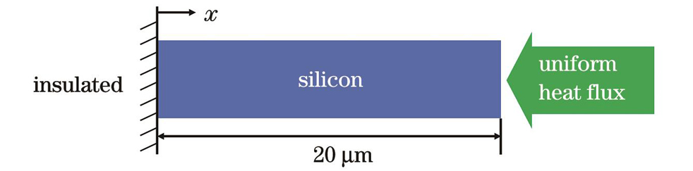
    Fig. 1. Schematic of one-dimensional silicon irradiated by femtosecond laser pulse
    Variation of electron density on silicon surface under femtosecond pulse irradiation
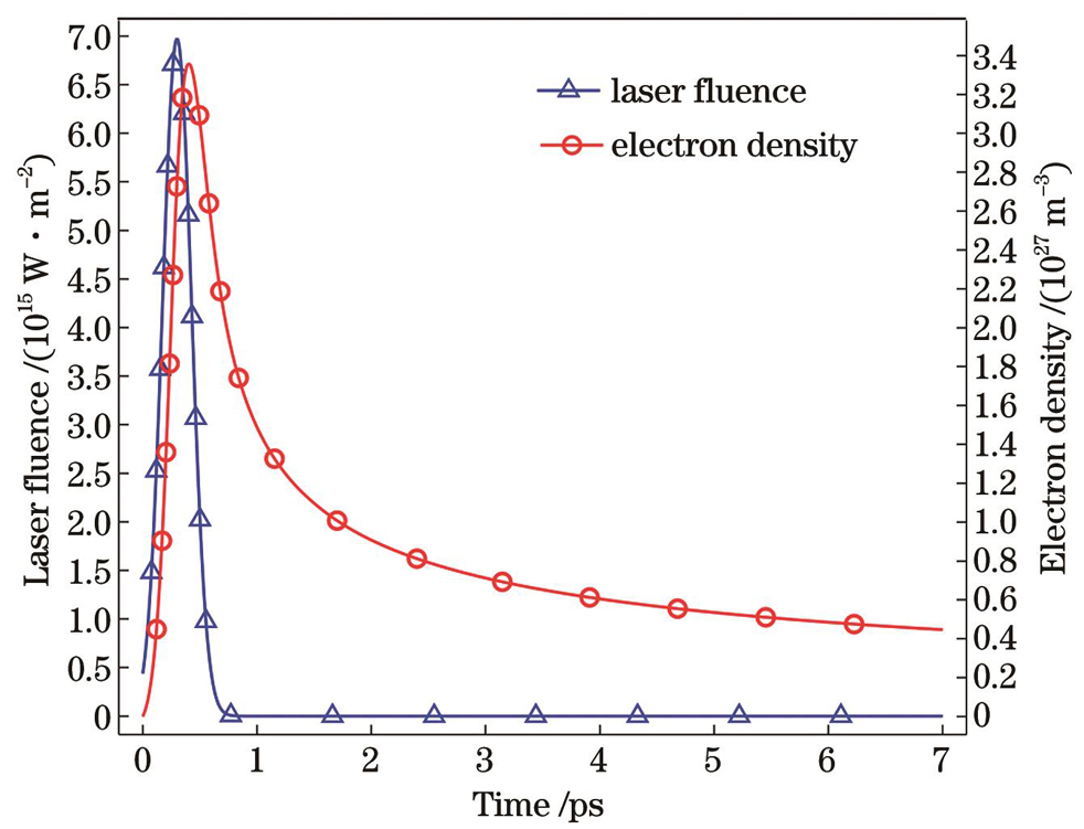
    Fig. 2. Variation of electron density on silicon surface under femtosecond pulse irradiation
    Temperature evolution of electron and lattice systems
    Fig. 3. Temperature evolution of electron and lattice systems
    Evolution of thermal conductivity of system
    Fig. 4. Evolution of thermal conductivity of system
    Comparison of multiple scanning process of Gaussian spot and single scanning process of flat top spot. (a) Multiple scanning process of Gaussian spot; (b) single scanning process of flat top spot
    Fig. 5. Comparison of multiple scanning process of Gaussian spot and single scanning process of flat top spot. (a) Multiple scanning process of Gaussian spot; (b) single scanning process of flat top spot
    Comparison of flat-top Gaussian distribution functions with different orders
    Fig. 6. Comparison of flat-top Gaussian distribution functions with different orders
    Ablative crater shapes under different laser pulse numbers. (a) 1 pulse; (b) 5 pulses; (c) 10 pulses
    Fig. 7. Ablative crater shapes under different laser pulse numbers. (a) 1 pulse; (b) 5 pulses; (c) 10 pulses
    Ablation crater depth versus laser fluence
    Fig. 8. Ablation crater depth versus laser fluence
    Optical path diagram of flat-top laser grooving experiment
    Fig. 9. Optical path diagram of flat-top laser grooving experiment
    Spot overlap rate and spot interval during flat top spot scanning
    Fig. 10. Spot overlap rate and spot interval during flat top spot scanning
    Groove surface and bottom images at same location
    Fig. 11. Groove surface and bottom images at same location
    2D groove shape test result
    Fig. 12. 2D groove shape test result
    ParameterValue
    Absorption coefficient α /(106 m-11.22
    Initial electron density Neq /(1012 cm-11.00
    Auger recombination coefficient γ /(10-43 m6·s-13.80
    Table 1. Material parameters
    ParameterValue
    Wavelength λ /nm517
    Pulse duration tp /fs250
    Reflectivity R0.72
    Peak power density I0 /(1016 W·m-21.18
    Table 2. Laser related parameters
    Zhe Zhang, Qi Song, Kunpeng Zhang, Mei Xue, Yu Hou, Zichen Zhang. Simulation and Experimental Research on Flat Top Femtosecond Laser Grooving of Silicon Wafer[J]. Chinese Journal of Lasers, 2023, 50(20): 2002202
    Download Citation