Silicon is an important material utilized in various fields, such as biology and energy, particularly in the realm of integrated circuits. With advancements in semiconductor manufacturing toward large formats and thin substrates, the wafer-edge chipping and damage caused by traditional blade dicing have become increasingly significant in the field of semiconductor packaging. The introduction of low-dielectric-constant materials in the 90 nm integrated circuit technology node has presented a significant challenge to wafer dicing processes. The industry has responded by implementing a combination of laser surface grooving and mechanical dicing to address the low-dielectric-constant material separation issue. Laser processing equipment manufacturers have redirected their focus from nanosecond laser processing equipment toward ultrafast laser processing equipment that offers reduced thermal affected zones. However, existing research mainly focuses on optimizing the laser power, frequency, defocus, and feed speed, and comparatively analyzes multi-beam laser scribing spot distributions. A comprehensive theoretical analysis remains lacking. To address this gap, the current study utilizes a 517 nm femtosecond laser as a light source and shapes the energy of the focal spot into a flat-top distribution via a diffractive optical element for the surface grooving of silicon materials. The mechanism and quality of the groove process are investigated and discussed.
The experimental setup comprises a diode-pumped femtosecond fiber laser as the light source, while a galvanometer and an F-theta lens served as the beam movement and focusing tools. A diffractive optical element (DOE) is used to shape the near-focus spot into a top-hat square distribution on the surface of silicon for grooving. First, a one-dimensional simulation model is established using finite element analysis software, and the dual-temperature model is coupled with the excess carrier balance equation to analyze the interdependence among the material electrons, lattice, and carrier density in the femtosecond laser ablation process. This results in the establishment of a theoretical model for the femtosecond laser ablation process for silicon materials. Subsequently, a two-dimensional simulation model is established to simulate the morphology evolution during the silicon laser ablation process, and the impact of multipulse lasers with different spot intervals and energies on the groove quality is calculated. Finally, an experimental optical system is constructed for the grooving experiments, and the actual morphology is tested using a laser confocal microscope and the results are compared with those of the two-dimensional simulation.
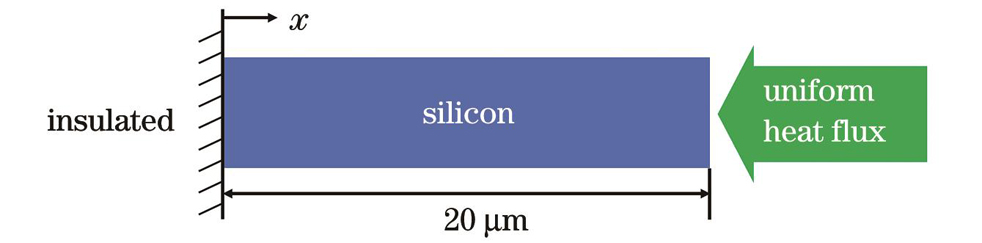
The one-dimensional model (Fig. 1) demonstrates that the temperature of the free electrons in the silicon material increases rapidly during the 517 nm femtosecond laser irradiation, reaching a maximum temperature of approximately 28000 K, while the lattice temperature remains constant. The energy of the electrons is transferred to the lattice system after the laser pulse, causing the temperature of the electrons to decrease and that of the lattice to increase (Fig. 2). This suggests that the femtosecond laser primarily damages the silicon material through electron excitation, thereby achieving "cold" processing and reducing thermal damage to the material. The two-dimensional model (Fig. 7) demonstrates that ablation occurs when the laser flux exceeds 0.3 J·cm-2 and the ablation depth increases significantly. The simulation results indicate that the thermal effect of the femtosecond laser ablation is small when the luminous flux is below 1.5 J·cm-2, and the ablation depth remains relatively stable (Fig. 8). The experimental results confirm that the top-hat square spot produces a flat-bottomed inverted trapezoidal groove with a width of approximately 35 μm and a depth of approximately 16 μm (Fig. 11). The sidewalls of the grooves are vertical and their shapes are consistent. However, the actual groove depth is slightly smaller than the depth calculated from the two-dimensional simulation model owing to the non-ideal fluence distribution of the light spot and the presence of plasma clusters generated during processing. These results indicate that the model produces better results with fewer processing pulses.
This study proposes the use of a DOE element to shape a femtosecond Gaussian spot with a wavelength of 517 nm into a top-hat square spot to achieve laser grooving on silicon surfaces. First, a theoretical model for the femtosecond laser ablation of silicon materials is established. The simulation results demonstrate that the femtosecond laser can excite a significant number of free electrons within the pulse duration, causing the electronic system temperature to surpass the damage threshold, while the crystal lattice temperature remains constant. A flat-top Gaussian distribution function is utilized to establish a two-dimensional flat-top spot ablation model, and the laser single-pulse ablation depth is calculated. The results indicate that the ablation groove shape of the flat-top square spot closely resembles an inverted trapezoid, with a high energy utilization rate and a linear relationship between the ablation depth and the number of pulses when the number of pulses is small. A self-constructed silicon wafer femtosecond grooving system is used to adjust the grooving process by modifying the processing speed of the galvanometer and laser power at a constant laser frequency. Under the conditions of an incident light power of 22 W and a stage speed of 2000 mm/s, silicon wafer grooving is obtained with a high groove bottom level, good side wall verticality, and a depth of 16 μm. The experiments demonstrate that the use of flat-top laser grooving significantly improves the processing efficiency and spot utilization, with a flat groove bottom and vertical side wall, which are advantageous for subsequent processing technologies.