• Advanced Photonics Nexus
  • Vol. 2, Issue 4, 044001 (2023)
Kunping Guo1、2、*, Zhe Tang1, Xingxing Chou3, Saihu Pan4, Chunchen Wan1, Tao Xue1, Liping Ding1, Xiao Wang1, Jin Huang1, Fanghui Zhang1、*, and Bin Wei5、*
Author Affiliations
  • 1Shaanxi University of Science and Technology, School of Electronic Information and Artificial Intelligence, Xi’an, China
  • 2University College London, Department Physics and Astronomy and London Centre for Nanotechnology, London, United Kingdom
  • 3Shaanxi University of Science and Technology, School of Electrical and Control Engineering, Xi’an, China
  • 4Changzhou University, School of Microelectronics and Control Engineering, Changzhou, China
  • 5Shanghai University, Ministry of Education, Key Laboratory of Advanced Display and System Applications, Shanghai, China
  • show less
    DOI: 10.1117/1.APN.2.4.044001 Cite this Article Set citation alerts
    Kunping Guo, Zhe Tang, Xingxing Chou, Saihu Pan, Chunchen Wan, Tao Xue, Liping Ding, Xiao Wang, Jin Huang, Fanghui Zhang, Bin Wei. Printable organic light-emitting diodes for next-generation visible light communications: a review[J]. Advanced Photonics Nexus, 2023, 2(4): 044001 Copy Citation Text show less
    Schematic illustration of OLED and OVLC applications. (a) Flexible and wearable OLED displays (Source: Fiere Electronics;14" target="_self" style="display: inline;">14 Lifewire15" target="_self" style="display: inline;">15). (b) Indoor environment for the VLC-based smart home. (c) Vehicular VLC system.
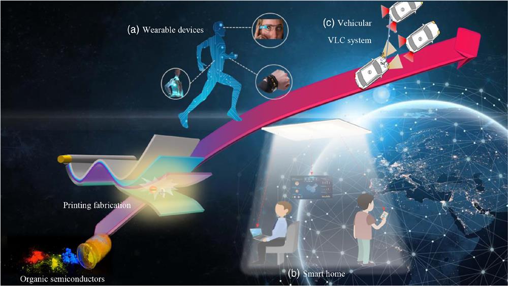
    Fig. 1. Schematic illustration of OLED and OVLC applications. (a) Flexible and wearable OLED displays (Source: Fiere Electronics;14 Lifewire15). (b) Indoor environment for the VLC-based smart home. (c) Vehicular VLC system.
    (a) 3D crystal structure of GaN. (b) Chemical structure of MDMO-PPV. (c) Schematic of metal organic frameworks (MOFs) in mixed-matrix membranes for VLC. Reproduced and adapted with permission from Ref. 28, ©2022 American Chemical Society. (d) Schematic of a typical quantum dot (QD) (Source: AVS Forum29" target="_self" style="display: inline;">29). (e) 3D crystal structure of a perovskite with the general formula ABX3. Reproduced and adapted with permission from Ref. 30, ©2017 Wiley-VCH Verlag GmbH & Co. KGaA, Weinheim.
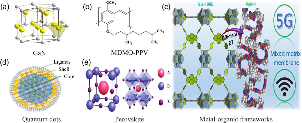
    Fig. 2. (a) 3D crystal structure of GaN. (b) Chemical structure of MDMO-PPV. (c) Schematic of metal organic frameworks (MOFs) in mixed-matrix membranes for VLC. Reproduced and adapted with permission from Ref. 28, ©2022 American Chemical Society. (d) Schematic of a typical quantum dot (QD) (Source: AVS Forum29). (e) 3D crystal structure of a perovskite with the general formula ABX3. Reproduced and adapted with permission from Ref. 30, ©2017 Wiley-VCH Verlag GmbH & Co. KGaA, Weinheim.
    (a) Schematic illustration of chitin nanofiber transparent paper for flexible green electronics. Adapted with permission from Ref. 63, ©2016 Wiley-VCH Verlag GmbH & Co. KGaA, Weinheim. (b) Transfer process of the OLED tattoo device and picture presenting working OLED tattoo transferred on an organic as well as a PVF nanosheet. Reproduced and adapted with permission from Ref. 64, ©2021 Wiley-VCH Verlag GmbH & Co. KGaA. (c) Schematic illustration of the photodynamic therapy (PDT) treatment principle and a photo of the wearable OLED-based PDT patch. Reproduced and adapted with permission from Ref. 65, ©2020 American Chemical Society.
    Fig. 3. (a) Schematic illustration of chitin nanofiber transparent paper for flexible green electronics. Adapted with permission from Ref. 63, ©2016 Wiley-VCH Verlag GmbH & Co. KGaA, Weinheim. (b) Transfer process of the OLED tattoo device and picture presenting working OLED tattoo transferred on an organic as well as a PVF nanosheet. Reproduced and adapted with permission from Ref. 64, ©2021 Wiley-VCH Verlag GmbH & Co. KGaA. (c) Schematic illustration of the photodynamic therapy (PDT) treatment principle and a photo of the wearable OLED-based PDT patch. Reproduced and adapted with permission from Ref. 65, ©2020 American Chemical Society.
    (a) Schematic structure of the OLEDs. (b) Schematic illustration of phosphor-doped WOLED with conventional fluorescent host. (c) Schematic illustration of phosphor-doped WOLED with exciplex host. (d) Schematic diagram of all-TADF WOLEDs. (e) Schematic illustration of flexible WOLED structure based on PEAN and corresponding photograph of large-area WOLED with the size of 5 cm×5 cm. Reproduced and adapted with permission from Ref. 66, ©2014 American Chemical Society. (f) Schematic illustration of a tandem WOLED composed of orange and blue emitting units. Reproduced and adapted with permission from Ref. 67, ©2012 WILEY-VCH Verlag GmbH & Co. KGaA, Weinheim.
    Fig. 4. (a) Schematic structure of the OLEDs. (b) Schematic illustration of phosphor-doped WOLED with conventional fluorescent host. (c) Schematic illustration of phosphor-doped WOLED with exciplex host. (d) Schematic diagram of all-TADF WOLEDs. (e) Schematic illustration of flexible WOLED structure based on PEAN and corresponding photograph of large-area WOLED with the size of 5  cm×5  cm. Reproduced and adapted with permission from Ref. 66, ©2014 American Chemical Society. (f) Schematic illustration of a tandem WOLED composed of orange and blue emitting units. Reproduced and adapted with permission from Ref. 67, ©2012 WILEY-VCH Verlag GmbH & Co. KGaA, Weinheim.
    (a) The number of scientific publications related to organic VLC published over the past 15 years as counted by the Web of Science, as of October 28, 2022. Search criteria were set to “visible light communication” and “organic.” (b) Trends of data rates versus publication years. (c) Photographs of the blue OLEDs and the corresponding images under a microscope. Reproduced and adapted with permission from Ref. 22, ©2020 Springer Nature.
    Fig. 5. (a) The number of scientific publications related to organic VLC published over the past 15 years as counted by the Web of Science, as of October 28, 2022. Search criteria were set to “visible light communication” and “organic.” (b) Trends of data rates versus publication years. (c) Photographs of the blue OLEDs and the corresponding images under a microscope. Reproduced and adapted with permission from Ref. 22, ©2020 Springer Nature.
    (a) EQE-current density curves for the OLED. The electroluminescence (EL) spectrum is shown in the inset. (b) Eye diagrams characterized at 1 Mb/s with 1, 2.64, and 5 mA biases, as well as characterized at 2.4 Mb/s with 2.64 mA. (c) Block diagram of the experimental real-time VLC link. Reproduced and adapted with permission from Ref. 87, ©2020 Springer Nature.
    Fig. 6. (a) EQE-current density curves for the OLED. The electroluminescence (EL) spectrum is shown in the inset. (b) Eye diagrams characterized at 1  Mb/s with 1, 2.64, and 5 mA biases, as well as characterized at 2.4  Mb/s with 2.64 mA. (c) Block diagram of the experimental real-time VLC link. Reproduced and adapted with permission from Ref. 87, ©2020 Springer Nature.
    (a) Schematic presenting the deposition process of inkjet printing with separator. (I1,I2) photoluminescence microscopy imaging of QDs array with luminescent inks containing 100% and 90% cyclohexylbenzene; (I3,I4) higher resolution photoluminescence microscopy imaging of a single dot corresponding to I1 and I2. (b) Schematic view of the proposed process for slot-die roll coating. (c) Illustration of the top and front view of blade-coating process for fabricating multicolor polymer OLEDs. (d) Image of a completed 3D-printed OLED display. Reproduced and adapted with permission from: (a) Ref. 109, ©2017 American Chemical Society; (b) Ref. 100, ©2012 Springer Nature; (c) Ref. 110, © 2017 Wiley-VCH Verlag GmbH & Co. KGaA; (d) Ref. 111, © 2022 AAAS.
    Fig. 7. (a) Schematic presenting the deposition process of inkjet printing with separator. (I1,I2) photoluminescence microscopy imaging of QDs array with luminescent inks containing 100% and 90% cyclohexylbenzene; (I3,I4) higher resolution photoluminescence microscopy imaging of a single dot corresponding to I1 and I2. (b) Schematic view of the proposed process for slot-die roll coating. (c) Illustration of the top and front view of blade-coating process for fabricating multicolor polymer OLEDs. (d) Image of a completed 3D-printed OLED display. Reproduced and adapted with permission from: (a) Ref. 109, ©2017 American Chemical Society; (b) Ref. 100, ©2012 Springer Nature; (c) Ref. 110, © 2017 Wiley-VCH Verlag GmbH & Co. KGaA; (d) Ref. 111, © 2022 AAAS.
    (a) Diagram of the experimental setup used for the all-organic VLC system, adapted with permission from Ref. 98, © 2014 IEEE. (b) Photograph image of the main experimental setup of the all-organic flexible VLC link, adapted with permission from Ref. 99, ©2018 Multidisciplinary Digital Publishing Institute.
    Fig. 8. (a) Diagram of the experimental setup used for the all-organic VLC system, adapted with permission from Ref. 98, © 2014 IEEE. (b) Photograph image of the main experimental setup of the all-organic flexible VLC link, adapted with permission from Ref. 99, ©2018 Multidisciplinary Digital Publishing Institute.
    MethodMaterial UtilizationFilm QualityDepositionLarge-area CapabilityFeatureRef.
    Spin coatingLowNonuniformOn demandChallengingOff-center, ease fabrication88
    Microtransfer printingHighUniformOn demandGoodAccurate, microtransfer printing98
    Screen printingLowUniformOn demandGoodHigh accuracy, partially printing96
    Inkjet printingHighUniformOn demandGoodHigh accuracy, direct writing99
    Slot-die coatingHighHomogeneousContinuousHigh throughputFault-tolerant >1  μm thick, suitable for roll-to-roll100
    Blade coatingHighHomogeneousContinuousHigh throughputRapid drying, suitable for roll-to-roll101
    Table 1. Comparison of different solution-processed technologies.
    Kunping Guo, Zhe Tang, Xingxing Chou, Saihu Pan, Chunchen Wan, Tao Xue, Liping Ding, Xiao Wang, Jin Huang, Fanghui Zhang, Bin Wei. Printable organic light-emitting diodes for next-generation visible light communications: a review[J]. Advanced Photonics Nexus, 2023, 2(4): 044001
    Download Citation