Abstract
Visible light communication (VLC) is an emerging technology employing light-emitting diodes (LEDs) to provide illumination and wireless data transmission simultaneously. Harnessing cost-efficient printable organic LEDs (OLEDs) as environmentally friendly transmitters in VLC systems is extremely attractive for future applications in spectroscopy, the internet of things, sensing, and optical ranging in general. Here, we summarize the latest research progress on emerging semiconductor materials for LED sources in VLC, and highlight that OLEDs based on nontoxic and cost-efficient organic semiconductors have great opportunities for optical communication. We further examine efforts to achieve high-performance white OLEDs for general lighting, and, in particular, focus on the research status and opportunities for OLED-based VLC. Different solution-processable fabrication and printing strategies to develop high-performance OLEDs are also discussed. Finally, an outlook on future challenges and potential prospects of the next-generation organic VLC is provided.1 Introduction
Organic semiconductors as a promising class of optoelectronic materials have attracted significant interest because of their fascinating physical–chemical properties, simple fabrication scheme to afford wearable or flexible devices, much wider scopes for easy production, and shaping and tuning of semiconductor properties compared to inorganic materials, such as silicon (Si).1,2 At present, a number of organic semiconductor classes based on small molecules and polymers have been discovered and widely used for next-generation organic and hybrid optoelectronics, such as organic thin film transistors, organic photodiodes, organic solar cells, and organic light-emitting diodes (OLEDs).3–5
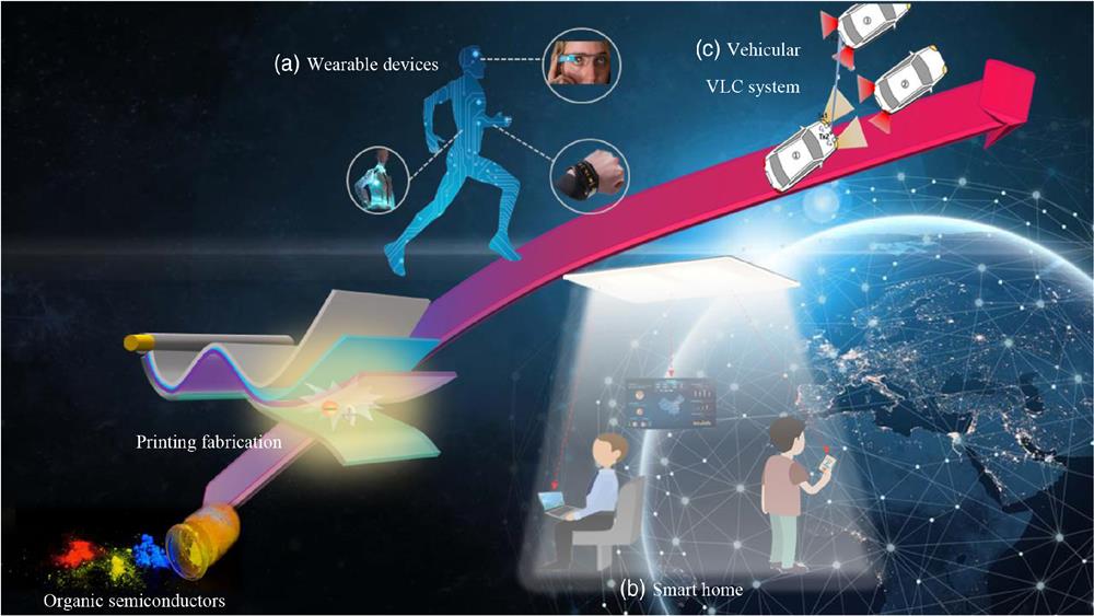
In lighting sources in particular, OLEDs have brought the initial studies to successful commercialization by exploiting both device engineering and organic semiconductor materials to push forward to achieve high luminous efficiency, ideal color quality, low operating voltages, as well as a long lifetime.6–8 In fact, OLEDs are attracting great interest for a variety of applications, spanning from high-resolution displays, solid-state lighting to automobiles, and augmented reality.9 OLEDs have many desirable properties, such as wide emission color tunability, low power consumption, and eco-friendliness.10 Considering the intrinsic high solubility of organic semiconductors in organic solvents, many efforts on the systematic investigation and optimization of the printing process have been made to realize efficient and large-area OLEDs.11–13 And the next-generation printable techniques are driving OLED innovations toward cost-efficient wearable devices. Figure 1(a) shows representative examples of future wearable display devices, that is, starting from smart glasses to enable augmented reality (i.e., displaying information additively over the natural scene behind glasses or lenses) to display vital signs or other health information measured by a smart watch in real time.16 More interestingly, fabric-based OLEDs are excellent candidates for clothing-type displays that are capable of flexing and bending with the human body.17 Concurrently, visual information presentations are among the key parts of wearable flexible electronics, allowing communication between a wearer and wearable appliances.18

Figure 1.Schematic illustration of OLED and OVLC applications. (a) Flexible and wearable OLED displays (Source: Fiere Electronics;14 Lifewire15). (b) Indoor environment for the VLC-based smart home. (c) Vehicular VLC system.
Envisioning the optical communication system developments, visible light communications (VLCs) offer significant advantages, e.g., license-free operation, physical-layer security, dual illumination, and wireless data communications. Such an intriguing feature for VLCs is strong enough to compete with other rival counterparts.19 This is appealing and potentially a “game-changer” for the next-generation (6G) internet of things (IoT) connectivity, which represents the network of physical objects, sensors within a world of interconnected devices, such as environmental monitoring, smart homes, display-to-display, and enabling objects to collect and exchange data.20 For the current VLC system, the typical Si-based LEDs and new organic compound-based OLEDs, which are generally applied as lighting sources in offices, schools, and homes, can be taken into account.21 As OLEDs are maturing from academic research into industrial development, it is thought that OLED lighting will eventually replace existing lighting sources, such as fluorescent and LED lamps. Currently, VLC systems integrating OLED as both lighting source and transmitter bandwidth have been demonstrated by Yoshida et al.,22 with free-space data transmission rates exceeding over a distance of 2 m due to the leveraging of active area size, emitting material, and the electrode design, which are high enough to support on-chip interconnects and secure communications (e.g., with the aim of IoT scenarios).
Sign up for Advanced Photonics Nexus TOC. Get the latest issue of Advanced Photonics Nexus delivered right to you!Sign up now
For an indoor environment, VLC systems offer broad area coverage to users applying room illumination and wide coverage using a beam-steered link,23 allowing many attractive services, such as emergency alarm broadcasting, localization-based services, smart community monitoring systems (smart illumination, smart multipurpose clocks, and smart sweeping robots), as well as multimedia transmission for entertainment (television, laptop, cell phone, etc.),24 as illustrated in Fig. 1(b). For outdoor scenarios, the field of applications is also expanding. In the automotive field, the first cars that use OLED sources are now beginning to appear due to the great number of possibilities it gives in terms of new aesthetic solutions and the possibility of realizing highly homogenous lighting functions.25 In this case, the vehicle-to-vehicle-based VLC system can connect via OLED head and taillights [Fig. 1(c)]. Simultaneously, traffic signal lights can be potentially used for functional communication between vehicles and infrastructure by means of VLC links as well,26 which play a key role in passing relevant information to the driver, analyzing traffic information in real time, and so on.27
This review first focuses on very recent advances of emerging semiconductor materials for LED sources in VLC, and then examines the motivations for OLED in future optical communication, with special attention to different approaches to achieving high-performance white OLEDs, their research status, and opportunities for the use of OLED-based VLC (OVLC). In addition, scalable fabrication techniques toward roll-to-roll manufacturing for direct-printed OLEDs are reviewed. Finally, we explore efforts to create flexible all-organic VLC. Envisioning a bright future for this technology, we further discuss the new opportunities and challenges offered by the next-generation OVLC link.
2 Emerging Semiconductor Materials for Optical Sources
Various types of semiconductor materials have been applied in light sources, such as indium gallium arsenide (InGaAs), aluminium oxide (), and gallium nitride (GaN). Among these candidates, wide bandgap GaN (3.4 eV) is one of the most popular subjects of investigations after Si in the semiconductor industry. Due to the Wurtzite crystal structure of GaN at room temperature [see Fig. 2(a)], polarization-induced electric fields can effectively affect the carrier recombination dynamics and thus offer fascinating properties for applications in optoelectronic devices.31,32 Notably, GaN-based LEDs as an attractive optical source become the popular choice for use in VLC systems because they can be modulated more greatly and faster than typical fluorescent or incandescent light sources, and particularly are easily amenable to integration with advanced drive electronics.33 Benefiting from the high electrical-to-optical bandwidth, the transmission rate of the VLC based on microsized LEDs via the nonreturn to zero coding has reached up to 1 Gbps. And the data rates of multi-Gbps were also indicated using advanced optical modulation formats.34 For example, Tsonev et al.35 reported transmission data beyond for LED-based VLC links by applying orthogonal frequency-division multiplexing (OFDM). Later, Islim et al.36 demonstrated an unprecedented data rate of for the LED-based VLC with bit-loading OFDM.
Figure 2.(a) 3D crystal structure of GaN. (b) Chemical structure of MDMO-PPV. (c) Schematic of metal organic frameworks (MOFs) in mixed-matrix membranes for VLC. Reproduced and adapted with permission from Ref. 28, ©2022 American Chemical Society. (d) Schematic of a typical quantum dot (QD) (Source: AVS Forum29). (e) 3D crystal structure of a perovskite with the general formula . Reproduced and adapted with permission from Ref. 30, ©2017 Wiley-VCH Verlag GmbH & Co. KGaA, Weinheim.
In contrast, organic semiconductors, quantum dots (QDs), or halide perovskites [Figs. 2(b)–2(d)] function as an emitting layer that is sandwiched between two thin charge-transporting layers to form an attractive flat-type LED source. These materials have emerged as a vibrant field spanning chemistry, materials science, physics, and engineering.37 Also, they are capable of interacting with photos, transporting electronic charge, and presenting semiconductor properties similar to typical inorganic materials such as Si. The significant progress in these fields has been pushed by the expectation to achieve numerous new applications, e.g., flexible/wearable displays, large-area illumination, low-power integrated circuits, as well as implantable bioelectronic devices.38–41
Organic chemistry provides solutions for tailoring semiconductor materials’ optoelectronic properties by exploiting the molecular/monomeric groups,42–44 enabling organic semiconductors tot be soft, lightweight, and mechanically flexible.45 In particular, since Tang46 first reported the organic electroluminescent diode, intensive research has been devoting novel semiconducting technologies to new product development and commercialization. Material science has developed fluorescence, phosphorescence, as well as third-generation thermally activated delayed fluorescence (TADF) emitters for LG and Samsung for commercial OLED production.47 At present, the mainstream mid- to high-end display markets for applications in small and medium sizes, such as cell phones, tablets, and fashion smart watches, are becoming dominated by OLED technology. Concurrently, OLEDs are becoming widespread in solid-state lighting markets, for instance, architectural lighting, automotive production, and aerospace. Following the commercial success of OLEDs for solid-state display, it is very exciting to further exploit OLED light sources as the transmitters for VLC links, and this strategy is becoming a research hotspot in recent years.48 In fact, not only small molecule, polymer materials-based OLEDs have been used for VLC but also the novel metal-organic frameworks (MOFs) have provided a strategy for designing high-speed VLC. Early this year, Wang et al.28 reported the luminescent MOF-based mixed-matrix membranes with an excellent modulation bandwidth of . Notably, the energy transfer enabled the communication data to increase from 132 to by changing from pure polymer to mixed-matrix membranes [Fig. 2(c)].
Inspired by the findings in semiconductor nanocrystals, - or -based colloidal semiconductor QDs have emerged asanother candidate for efficient LEDs. Nowadays, QD-based LEDs (QLEDs) have become close to standard for commercial applications, thanks to the development of QD synthesis and device engineering. Such LEDs generally show very pure and saturated colors with a narrow spectral bandwidth of the electroluminescence emission of .49 QDs are quasispherical nanocrystals composed of tens to a few thousand atoms and most QDs consist of three parts: core, shell, and ligands, as shown in Fig. 2(d). Importantly, QDs have large surface area-to-volume ratio characteristics, allowing the precise composition of each part and enabling the shell thickness to affect their behavior.50 Namely, the bandgap of QDs related to light absorption, bright emission, and electronic transport can be easily tuned by varying their size as well as composition. In addition, QDs can be combined with inorganic LEDs to form hybrid sources for VLC. Recently, Leitao et al.51 reported free-space VLC links above 10 cm at transmission rates in excess of by utilizing QDs as color-converting blue InGaN LEDs.
A more recent addition to the family of promising LEDs is a device incorporating hybrid organic–inorganic halide perovskites. Such materials have a general crystal structure [see Fig. 2(e)], where A is a monovalent cation, typically organic formamidinium , methylammonium (), as well as inorganic cesium; B is the divalent metal cation (e.g., lead, tin); X is a halide anion.30,52 Their optoelectronic properties are easily changed by regulating the site ions of A, B, or X or exploiting multicomponent A, B, or X ions to achieve their specific applications. Similar to traditional semiconductor materials, the electroluminescent performance originating from excited charge carriers in perovskites is dominated by both nonradiative and radiative processes.53 Since the first demonstration of bright perovskite LEDs (PeLEDs),54 device external quantum efficiencies (EQEs) have increased from less than 1% to more than 20%.55–57 This impressive progress puts the PeLEDs in the same league as more mature OLED or QLED technologies.
3 OLED Transmitter for VLC
3.1 Motivations for OLED Light Source
It is important to note here that toxic elements, such as lead, antimony, and gallium, are widely used to develop highly efficient LEDs, whereas their disposal remains an issue that raises a range of environmental concerns, particularly if there is subsequent disposal on land or water bodies. Therefore, safety hazards and possible risks to the environment are an urgent need to be considered and effectively overcome. In terms of the prototype optoelectronic devices development, one of the targets for researchers is to match sustainability requirements, with an emphasis on materials that do not negatively harm both environment and humans. Instead of traditional semiconductors materials, there is a huge interest in adopting semiconductors with nontoxic or less toxic elements. For example, colloidal QDs of ternary and semiconductors as well as quantum-sized (i.e., ) carbon dots as environmentally friendly alternatives to more traditional -based QDs in LEDs have been reported,58,59 although recent efforts have been made to studying new alternatives to perovskite materials by leveraging nontoxic elements (e.g., Bi, Sn, and Cu) with organic compounds.60 Nevertheless, the performance of LEDs containing these materials is not comparable with the devices using metal-containing organic compounds or purely organic semiconductors.
Nontoxic organic materials have become the subject of industrial and academic research interest as extremely attractive candidates8 because of the promise of their cost-effective production and potential sustainability.3 Baumann’s group investigated semiconductor materials and processes applied in OLED fabrication from the view of sustainability and discussed the upcoming trends afterward.61 Volz62 reviewed TADF OLEDs for energy-efficient sustainable light sources and displays. Using crystalline chitin nanofibers as a biodegradable substrate, Jin et al.63 fabricated a flexible OLED device and demonstrated its potential for flexible green electronics, as illustrated in Fig. 3(a). In the meantime, Barsotti et al.64 created a novel ultrathin, green OLED that can be applied to skin like a children’s transfer tattoo; this could be used to fabricate fashion—for instance, providing light-emitting fingernails and glowing tattoos. In this study, authors present an OLED tattoo transferred onto an orange and a freestanding polyvinyl formaldehyde (PVF) nanosheet (), as shown in Fig. 3(b).
Figure 3.(a) Schematic illustration of chitin nanofiber transparent paper for flexible green electronics. Adapted with permission from Ref. 63, ©2016 Wiley-VCH Verlag GmbH & Co. KGaA, Weinheim. (b) Transfer process of the OLED tattoo device and picture presenting working OLED tattoo transferred on an organic as well as a PVF nanosheet. Reproduced and adapted with permission from Ref. 64, ©2021 Wiley-VCH Verlag GmbH & Co. KGaA. (c) Schematic illustration of the photodynamic therapy (PDT) treatment principle and a photo of the wearable OLED-based PDT patch. Reproduced and adapted with permission from Ref. 65, ©2020 American Chemical Society.
Within this context, organic semiconductor-based OLEDs are expected to advance greater goals without taking into account the need to satisfy environmentally friendly and human health issues, for instance, integrating OLED device into the periphery of the people’s body for health care or leisure applications. Jeon et al.65 presented a flexible parallel-stacked OLED for wearable photodynamic therapeutic application [see Fig. 3(c)] and as a wearable display. The fabricated OLED exhibited a significant 24% decrease in the cancer cell viability after a short time of 0.5 h irradiation. Furthermore, OLEDs are now explored for wearable sensing by combing organic photodiodes to enable higher flexibility and miniaturization and eventually achieve “imperceptible” sensors. Thus, this trend is not only allowing OLED to revolutionize the light-emitting application but also will challenge the deployment of the emerging VLC technology.
3.2 High-performance white OLED
A high-efficiency white OLED (WOLED) has been the long-term aim for solid-state lighting. For the OVLC scenarios, WOLED with a higher EQE (i.e., toward lower power consumption under the same driving voltage) will provide a longer and more stable transmission distance. In general, the architecture of OLED includes an indium-tin-oxide (ITO) coated glass, hole transport layer, emissive layer, electron transport layer, and a metallic cathode, as illustrated in Fig. 4(a). In terms of white light, the single-emitting-layer WOLED has attracted significant attention due to the reduced structural complexity, low manufacturing cost, as well as feasible all-solution processing. One of the most straightforward ways is to use the single light-emitting molecules as an emissive layer, thanks to their unique advantages, such as good color stability and simple fabrication, to achieve WOLED. In fact, many light-emitting molecules have been reported by using intramolecular charge transfer, excited state proton transfer, excimer, etc. Unfortunately, most single-emitting molecule-based WOLED always exhibits poor device performance, thus limiting their further application.
Figure 4.(a) Schematic structure of the OLEDs. (b) Schematic illustration of phosphor-doped WOLED with conventional fluorescent host. (c) Schematic illustration of phosphor-doped WOLED with exciplex host. (d) Schematic diagram of all-TADF WOLEDs. (e) Schematic illustration of flexible WOLED structure based on PEAN and corresponding photograph of large-area WOLED with the size of . Reproduced and adapted with permission from Ref. 66, ©2014 American Chemical Society. (f) Schematic illustration of a tandem WOLED composed of orange and blue emitting units. Reproduced and adapted with permission from Ref. 67, ©2012 WILEY-VCH Verlag GmbH & Co. KGaA, Weinheim.
Alternatively, the doping strategy within a monochromatic emissive layer (namely, the single emissive layer incorporating multiple molecules) has become the subject of intense academic and industrial issues in recent years. It is widely known that white-light emission can be generated by blending either three emitters with primary colors [blue, green, and red (RGB)] or two emitters with complementary colors (blue and orange). Most activities are dedicated to phosphorescent guests that have been demonstrated to harvest 100% excitons in OLED. In particular, fluorescence–phosphorescence (F–P) hybrid WOLEDs have drawn great attention in recent years owing to their intriguing merits, such as good stability and high efficiency. Crucially, the choice of appropriate host material for WOLED plays an important role in maximizing exciton utilization and suppressing photon loss to improve device performance.
In most cases, the conventional fluorescent host materials are used for fabricating F–P hybrid WOLEDs. Such host materials, generally with higher triplet levels than that of the phosphorescent dopants, thereby inhabit the reverse energy transfer from the guest to the fluorescent matrix and allow for efficient Förster and Dexter energy transfer in the emitting layer of the OLEDs [see Fig. 4(b)]. For instance, Liu et al.68 reported a single-emissive-layer F–P hybrid WOLED by incorporating green and red phosphors into the novel blue fluorescence 4-(4,6-diphenoxy-1,3,5-triazin-2-yl)-N,N-diphenylaniline (POTA) host, achieving a maximum EQE of 24.7%. In 2019, near 100% exciton utilization and hybrid WOLED with a maximum EQE of 27.5% and power efficiency of were simultaneously achieved by doping yellow phosphor (PO-01) into a novel blue fluorescence host.69 Interestingly, the exciplex host has also drawn attention that not only takes into account the appropriate highest occupied molecular orbital/least unoccupied molecular orbital levels and high triplet level but also, crucially, has very low barriers, which are beneficial to improving carrier injection/transfer and thus obtaining highly efficient WOLED. Another attractive advantage is that the charge balance in the emissive layer can be effectively tuned by varying the donor-to-acceptor ratio [Fig. 4(c)]. For example, by utilizing an mCBP:B4PyPPM exciplex host, hybrid WOLED with EQE of 21% at high luminance of were demonstrated by Zhao et al.70 Such a device exhibited very stable white emission with Commission Internationale de L’Eclairage (CIE) coordinate changing range of as increasing luminance from 100 to . Very recently, all-organic WOLEDs based on noble metal-free TADF host and emitter materials were intensively studied.71–73 For the TADF host, low-energy triplet excitons can be converted to the radiative singlet state via an endothermic process of the reverse intersystem crossing, thereby harvesting both the singlet and triplet excitons for a nearly 100% internal quantum efficiency. As illustrated in Fig. 4(d), the long-range Förster energy from the singlet of host transferred to dopant molecules produced an orange emission, while the singlet energy that cannot be transferred to the guest molecules only generated blue emission, thus blending to produce the white emission in the device. With this strategy, Chen et al.74 first demonstrated all-TADF single-emitting-layer WOLEDs with 32.8% EQE, which surpassed the phosphorescence-based WOLEDs by then. It provides a new insight for exploiting high-performance pure organic white devices.
Apart from materials design, strategic device engineering as a significant way for WOLEDs has also been a focus.75,76 In a conventional WOLED, there is only of the total white emission that is outcoupled, whereas most generated radiation is lost by the substrate, evanescent, and waveguide mode.77 In this case, many methods, such as surface plasmons,78 subwavelength photonic crystals,79 and dielectric mirrors,80 have been investigated to enhance outcoupling efficiency and thus improve EQE in WOLEDs. One of the most prominent works is exploiting an optimized light outcoupling structure for simultaneously extracting light in substrate and waveguide modes,66 as shown in Fig. 4(e), flexible WOLEDs present a maximum and at luminance of . In addition, from the view of internal device structure modification, high-efficiency WOLEDs could also be obtained by using the tandem structure. Such devices are generally fabricated by vertically stacking RGB units or complementary units (blue and yellow) in series [Fig. 4(f)],67 where emitting units are interconnected via a charge generation layer. Beyond doubt, these techniques are beneficial to further improving commercial WOLED lighting products.
3.3 Status Quo of OVLC
As they rapidly increase in performance, low-consumption OLEDs are considered an attractive choice for VLC applications. In Fig. 5(a), we present the evolution of the number of scientific publications related to organic VLC published over the past 15 years. Here the obvious decline for this year can be understood by the search being conducted during the same year. It is clear that there is an increasing trend toward VLC incorporating organic compounds. As far as we all know, the first report on employing OLED light source into the VLC system was proposed by Punke et al.,81 which demonstrated data transmission, but with a plastic fiber connection. Minh et al.82 demonstrated a transmission rate over free space by employing an analog equalization approach. The fastest reported transmission data were exceeding in 2014, which was demonstrated by incorporating a novel poly[2-methoxy-5-(3′,7′-dimethyloctyloxy)-1,4-phenylenevinylene] (MDMO-PPV) for polymer OLED (PLED).83 Later, Chen et al.84 proposed a new data modulation scheme jointly with bit-power loading and channel postequalization. Blue OLED incorporating such a system achieved a data rate of .
Figure 5.(a) The number of scientific publications related to organic VLC published over the past 15 years as counted by the Web of Science, as of October 28, 2022. Search criteria were set to “visible light communication” and “organic.” (b) Trends of data rates versus publication years. (c) Photographs of the blue OLEDs and the corresponding images under a microscope. Reproduced and adapted with permission from Ref. 22, ©2020 Springer Nature.
The rapid growth of the reported transmitter rates is illustrated in Fig. 5(b). The state-of-the-art transmission rates incorporating different OLEDs over the last 10 years epitomize the rising attention to OVLC. A new recording rate was reached when Yoshida et al.22 examined the influencing factors limiting the bandwidth of OLEDs and how to cope with them, demonstrating that OLED sources could obtain wireless transmitter rates over in a practical length of 2 m. In Fig. 5(c), the authors show the OLEDs with different active areas, indicating that reducing OLED size and increasing driving voltage achieves high bandwidth. Despite such a high data rate for OVLC, this method cannot take advantage of the large area of the OLED source. Therefore, it is expected that future efforts on the OLED for OVLC will focus not only on a high data rate but also on large-area lighting.
3.4 OVLC Opportunities
Compared to the inorganic LED, OVLC transmitters are generally limited, owing to their lower modulation bandwidth. As demonstrated in previous literature,85,86 the root reason for OLEDs’ lower bandwidth stems from inherently low charge mobilities from to in organic semiconductor materials. Nonetheless, OVLCs are well suited to IoT applications, which only need a transmitter rate of a few megabits per second, or even less. More interestingly, extending the spectral range of OLED from the visible light into the near infrared (NIR) region can effectively expand the VLC bandwidth, which is also very promising for integrated NIR OVLC in many new applications by exploiting NIR radiation (e.g., wearable or implanted organic biosensors). Minotto et al.87 reported a far-red/NIR OLED with 650 to 800 nm emission region and EQE over 2.7% [see Fig. 6(a)], and then they demonstrated an error-free transmission rate [Fig. 6(b)], which is adequate to realize the indoor point-to-point connections.
Figure 6.(a) EQE-current density curves for the OLED. The electroluminescence (EL) spectrum is shown in the inset. (b) Eye diagrams characterized at with 1, 2.64, and 5 mA biases, as well as characterized at with 2.64 mA. (c) Block diagram of the experimental real-time VLC link. Reproduced and adapted with permission from Ref. 87, ©2020 Springer Nature.
Furthermore, it is noted that most reported OVLC generally requires a sophisticated electronic circuit, which will inevitably expand the specific surface area and influence the battery lifetime at the receiver. It is desirable for a practical VLC system to achieve high transmission speeds without equalization. Here, the authors used a simplified block diagram in Fig. 6(c), where two field-programmable gate arrays were embedded in the NI USRPs (which is a National Instruments universal software peripheral reconfigurable input-output).87 In fact, the “real-time” signal processing is very attractive, since the typical “offline” processing does not account for key issues in practical implementation, e.g., fixed-point signal processing, shared finite resources, and limited sampling frequencies.
4 Solution-processable Fabrication Strategies and Printing Techniques
Depositing functional material on a substrate via vacuum evaporation technology under an ultrahigh vacuum environment to fabricate organic electronic devices and organic molecules generally form amorphous thin films.88 Current thermal-evaporation systems generally combine a quartz-crystal thickness sensor/monitor with thickness options for co-evaporating two or more materials to form blends or doped films.75 In particular, thermal evaporation offers a straightforward fabricating multilayer structures strategy, enabling OLED to have a large variety of organic functional compounds and conductive electrodes.89,90 Although such advantages are now a cornerstone of the flat panel display industry, thermal evaporation is still plagued by low deposition rates, uniformity of the thickness on large area, and dependence on time- and cost-driven processes. Simultaneously, the in-line configurations could greatly improve the throughput of the deposition process,75,91 instead of the conventional process, which enables the device in and out of the chamber of the evaporation and generally slows down the fabrication. Hence, thermal evaporation processing probably limits the mass production of OLEDs.
In contrast, solution-processing techniques are a relatively mature technology to true cost-effective OLED preparation due to their tunable rheology and formulations. In addition, many of the most promising semiconducting materials, e.g., organic small molecules, polymers, and organic/inorganic nanoparticles,92 are now available in solution-processable formulations, thereby further expanding the reach of this deposition strategy. On the current lab-scale techniques, spin coating is extremely popular among device engineers and active researchers because of its simplicity and short processing time under ambient conditions. Unfortunately, there exist several disadvantages associated with this technology (for example, lack of lateral patterning capability and high solution wastage).93 From a scaling-up perspective, better solution-processable deposition techniques are urgently required for going from lab to fab scale. In this context, printing methods are among the most promising candidates thanks to their almost 100% material utilization, low-cost mass production, and simplified fabrication procedures (e.g., compared to the above thermal evaporation), as well as being economically and ecologically viable. Indeed, the low-temperature nature (e.g., a temperature “budget” of the process that can be strictly controlled to be below 150°C) of printing processes also enables a wide range of substrates for device fabrication, spanning from typical rigid and flat substrates to the wearable, flexible, and even stretchable ones, and thus opening the door for fabricating high-performance flexible optoelectronic devices.94 To date, a variety of printing techniques have been introduced for OLED fabrication, such as microtransfer printing95 and screen printing.96,97Table 1 shows a comparison of solution-processed spin coating and other printing methods for fabricating large-area OLEDs. The reason for this is that cost reduction can be obtained by employing high throughputs and high-volume production of prototype OLED panels on the flexible substrates. Here, we would like to capture the reader’s attention to inkjet printing, slot-die coating, and blade coating technologies, which provide a wealth of insight into the future roll-to-roll manufacturing for direct-printed OLEDs.
| Method | Material Utilization | Film Quality | Deposition | Large-area Capability | Feature | Ref. |
| Spin coating | Low | Nonuniform | On demand | Challenging | Off-center, ease fabrication | 88 |
| Microtransfer printing | High | Uniform | On demand | Good | Accurate, microtransfer printing | 98 |
| Screen printing | Low | Uniform | On demand | Good | High accuracy, partially printing | 96 |
| Inkjet printing | High | Uniform | On demand | Good | High accuracy, direct writing | 99 |
| Slot-die coating | High | Homogeneous | Continuous | High throughput | Fault-tolerant thick, suitable for roll-to-roll | 100 |
| Blade coating | High | Homogeneous | Continuous | High throughput | Rapid drying, suitable for roll-to-roll | 101 |
Table 1. Comparison of different solution-processed technologies.
4.1 Inkjet Printing
The inkjet printing method is a low-cost and fascinating process for the high-accuracy deposition of liquid inks. This technique is not only fundamental for graphic printing applications but has also attracted increasing attention as a liquid ink-based high accuracy, maskless, and noncontact deposition technology. Notably, inkjet-based direct writing technology provides the advantage of making the multilayer thin films easily changeable from batch to batch. In addition, the inkjet printing reduces material consumption and is easily scalable,99,102 which are clear advantages with respect to the conventional off-center spin-coating method.
In general, most types of printed organic/polymer LEDs still adopt ITO as the transparent conductive electrode, which is often structured and deposited by expensively photolithographic technologies. Moreover, the brittleness of ITO and the scarcity of indium further hinder the development and application of LEDs. Hence, the development of inkjet-printed (IJP) electrodes would stimulate the development and promote the scalability of this technique. However, when adopting the IJP process to fabricate bottom electrodes, the printed devices with thin-film thicknesses of several 100 nm have been shown to be challenging.103 Indeed, printed devices tend to present aninhomogeneous random rough surface with many defects or/and spikes after heat treatment of its metal precursor, resulting in the high-frequency leakage currents or electrical shorts in the device. To address such limitations, Kinner et al.103 and Hermerschmidt et al.104 proposed inkjet-printing methods of Ag nanoparticles combined with poly(3,4-ethylenedioxythiophene):poly(styrenesulfonate) (PEDOT:PSS) as an ITO replacement for ITO-free OLEDs. In addition, Pozov et al.105 investigated the less expensive material for the fabrication of the ITO-free electrode: they reported an IJP Cu nanoparticle grid blend with PEDOT:PSS as the bottom anode.
However, the “coffee-ring” effect for the printed film is the main drawback of such a technique, although pinholes and solvent orthogonality cannot be overlooked either.106,107 One strategy to minimize the coffee-ring patterns is to give a high substrate temperature, thus enabling the solvent to evaporate before the solution undergoes hydrodynamical spreading to form the undesired coffee ring.108 Another way to obtain coffee-ring-free and low roughness printed thin film was recently reported.109 As shown in Fig. 7(a), the thickness of functional layer was controlled by altering the concentration of semiconducting inks and turning the drop rates in a single pixel. By mixing decane and cyclohexylbenzene as solvents, the emitter dots showed better coverage and uniformity in distribution. These results pave the way for inkjet printing application to move toward the solution-processed pixelated QLEDs in the future.
Figure 7.(a) Schematic presenting the deposition process of inkjet printing with separator. photoluminescence microscopy imaging of QDs array with luminescent inks containing 100% and 90% cyclohexylbenzene; higher resolution photoluminescence microscopy imaging of a single dot corresponding to and . (b) Schematic view of the proposed process for slot-die roll coating. (c) Illustration of the top and front view of blade-coating process for fabricating multicolor polymer OLEDs. (d) Image of a completed 3D-printed OLED display. Reproduced and adapted with permission from: (a) Ref. 109, ©2017 American Chemical Society; (b) Ref. 100, ©2012 Springer Nature; (c) Ref. 110, © 2017 Wiley-VCH Verlag GmbH & Co. KGaA; (d) Ref. 111, © 2022 AAAS.
4.2 Slot-die Coating
Slot-die coating is an alternative fabrication strategy for large-area OLEDs, holding the promise of depositing large and homogenous thin films of functional materials with simultaneous coatings of multiple layers from different solutions.112 Notably, this technique is capable of depositing a vast range of thickness (i.e., from 20 nm to ) and coating a variety of process materials. Slot-die coating is very suitable for many new applications, including roll-to-roll, sheet-to-sheet, and sheet-on-shuttle processing.113 Sandström et al.100 reported a large-area flexible organic light-emitting device by using purpose-built slot-die coating equipment. Figure 7(b) schematically illustrates the successive deposition of the organic layer and anode electrode on the top flexible cathode-coated substrate, where it is mounted on a roll. The functional material is transferred from the external container to the slot-die head by a pump. In particular, the coating thickness for devices is determined by the substrate speed and the flow rate of ink. Although the roll-coated devices showed strong EL emission at low operating voltage, the functional layers were found to be highly uneven. Such a drawback enabling the control of the surface morphology and of the layer thickness becomes more challenging. In this context, Choi et al.114 investigated the slot-die coating process for fabricating large-size OLEDs. Improvements were obtained by decreasing the flow down of the PEDOT:PSS close to the inner perimeter of the insulator zone, the pinhole-like surface in the hole transport layer, and the dissolution between two different tandem layers. The slot-die coated hole-injection/hole-transport films showed peak-to-peak roughness of , thereby resulting in such processed OLEDs exhibiting similar performance levels as reference devices using spin-coated and vacuum-evaporated processes.
4.3 Blade Coating
Blade coating is a promising alternative to spin coating and inkjet printing for large-size OLEDs, thanks to the higher usage rate of materials, wide compatibility with different substrates, as well as constant deposition of large-area thin-films.115–117 Notably, blade coating allows depositing multiple layers with minimal crossdissolution. This advantage stems from a rapid drying process and is highly beneficial for fabricating multilayer OLEDs based on those materials with a limited solubility window, which usually suffer from solvent orthogonality issues in solution deposition.118 For example, Tseng et al.115 presented multilayer PLEDs using blade coating on a hot plate. Such methods enabled negligible film thickness variations (i.e., 3.3% on a 10 cm scale) as well as low film roughness (i.e., on the micrometer scale). From a performance point of view, the authors further demonstrated that blade coating-based bilayer devices exhibited more than double efficiency with respect to the single-layer spin-coated PLED. Later, Yeh et al.101 reported all-small-molecule multilayer OLEDs with a hole-transport layer, emitting layer, and electron transport layers using blade coating on a hot plate at 80°C with hot wind, thereby suggesting that common small molecules, originally aimed for vacuum evaporation, can be exploited to fabricate cost-effective multilayer OLEDs through blade coating.
Another example of blade coating was reported by Han et al.,110 who proposed an interesting surface energy patterning (SEP) method to fabricate multicolour PLEDs. The SEP critically reduced the amount of solution used, improved thin-film quality and enhanced the device reproducibility. As schematically shown in Fig. 7(c), by taking advantage of SEP to fabricate two different PLEDs, the authors achieved a multicolor PLED on the flexible substrate, which was the first known instance of printing multiple materials by blade coating. Interestingly, such devices were implemented in a wearable device, in conjunction with a photodiode, performing blood oxygenation on the human wrist. This result demonstrates how blade-coating technology could be used to develop all-printed wearable sensor applications.
4.4 3D Printing
3D printing or additive manufacturing is emerging as a promising technology for the rapid prototyping of advanced optoelectronic devices. Different from traditional methods of manufacturing products, 3D printing allows for fabricating optoelectronic devices with a wide range of materials: there is no sophisticated fabrication requirement (e.g., molds, stencils, photolithography), thereby offering substantial advantages, including the utilization of portable and cost-effective facility for customizable manufacture,119 seamless joints of diverse materials, printability on free-form and deformable surfaces,120 and a feature allowing the targeted product with a minimum number of intermediate steps.121 Among currently available 3D printing technologies, extrusion-based 3D printing is well adapted for fully printed functional devices, combining nanoscale ink print with manufactured macroscale devices.122 Moreover, a significant advantage would be appealing to integrate multiple 3D printed functionalities on typical rigid or wearable/flexible substrates.123,124
Current publications assert that partially printed OLEDs typically depend on spin coating or thermal evaporation to deposit specific components and fabricate functional layers, especially in terms of the electrodes and interconnects, which generally require vapor or sputtering deposition of materials (e.g., metals, metal oxides), to realize the high optical transmittance and electrical characteristics. Previously, scientists tried to 3D print OLED displays; however, it was quite challenging to obtain uniformity of the light-emitting layers. Eder et al.125 demonstrated a printed OLED that was fabricated on a 3D printer, but the dispensed top cathode, gallium indium tin-alloy (GaInSn), did not allow for conformal printing of electrical interconnects. Early this year, Su et al.111 demonstrated a multimodal printing strategy using extrusion merge with spray printing, manifesting fully 3D printed flexible OLED displays. The interconnects, insulation, electrodes, and encapsulation were successively extrusion-printed by a 3D printer, and the organic emission layers were spray-printed via the same one. Such an OLED display was inches (3.8 cm) on each side and had 64 pixels that all worked properly to emit light, as shown in Fig. 7(d). Such a fully 3D-printed OLED also showed a very stable EL emission after 2000 bending cycles, indicating its great potential in flexible electronics and wearables. This method opens the door to manufacturing cost-efficient OLEDs for VLC networks by means of commercial printers.
5 All-organic Flexible Optical Communication Systems
Incorporating organic electronic devices into VLC links is an attractive prospect for implementation in future communication links, driving all parts of the system toward flexibility, such as transmitters, receptors, and electronic drivers. Importantly, this further offer the possibility of integrating such devices into the exciting wearable clothes and industrial woven fabrics, as summarized by Hutter et al.126 To date, mostly organic semiconductors-based VLC systems have paid attention to either transmitter or receiver, instead of the all-organic VLC link, so as to obtain the maximum performance measure from each device. However, it is necessary to get further insight into the communication performance of a VLC system using the organic electronic device as both an optical transmitter and receiver. Haigh et al.127 first presented an all-organic VLC link by combining commercially available OLEDs as the transmitter and P3HT:PCBM-based organic photodetectors (OPDs) as the receiver, as shown in Fig. 8(a). The aim of that paper was to give the possibility of the free-space VLC system that can be manufactured entirely by all-organic semiconductors.
Figure 8.(a) Diagram of the experimental setup used for the all-organic VLC system, adapted with permission from Ref. 98, © 2014 IEEE. (b) Photograph image of the main experimental setup of the all-organic flexible VLC link, adapted with permission from Ref. 99, ©2018 Multidisciplinary Digital Publishing Institute.
Most interestingly, Vega-Colado et al.128 reported a flexible, fully organic VLC link by applying a flexible OLED (from LG Chem), a flexible OPD, and flexible printed circuit boards for the emitter/transmitter and receiver circuit, respectively [see Fig. 8(b)]. Such an all-organic VLC link was further operated in indoor conditions, and the audio signal for transmitting and receiving was of enough quality to be reproduced. This exciting result highlights the potential impact of printable OLED and OPD technologies for the fabrication of all-organic flexible VLC applications, which would benefit the wireless human-machine system by providing efficient human-to-machine communications.
Similar to the case of OLED, great efforts have been dedicated to the development of OPD. So far, the dark current and responsivity of the OPD are approaching that of Si-based PDs.129 Tavakkolnia et al.130 proposed a multiple-input multiple-output structure based on OPV and a single-channel structure, achieving data rates of 363 and , respectively. Unfortunately, implementing OPD for VLC is still challenging. For instance, the optical-to-electrical response speed of the OPD is generally limited owing to the slow charging and discharging processes. In 2022, Cho et al.131 applied a bulk heterojunction-based OPD to the receiver of a VLC, realizing a data rate. It is the highest data rate ever obtained on an OPD-based VLC.
6 Conclusions and Future Perspectives
VLC is the upcoming wireless communication technology, with the twofold benefit of exploiting the ultraviolet, visible, NIR, as well as infrared regions in the electromagnetic spectrum and significantly increasing data rates. As white LEDs were starting to emerge for energy-efficient greenhouse and intelligent street lighting, the commercial market adopting LED light sources as candidates for transmitters in optical data communications is inevitable. From this perspective, the current status of VLC was first reviewed in terms of existing inorganic counterparts and competing materials, including inorganic QDs and organic as well as hybrid organic–inorganic semiconductors for LEDs.
The advanced optoelectronic devices for future VLC applications are expected to be nontoxic, low-cost, high-speed, and easy to integrate. Due to the promise of cost-effective production and environmental sustainability, nontoxic organic materials-based OLEDs have become a hot topic in academic and industrial circles. Great progress has been made in the exploitation of emitting materials and device structure for WOLEDs, thereby stimulating efforts on OLED toward VLC. There is no doubt that OVLC for data transmission rates is not comparable to inorganic VLC links (e.g., ) incorporating LEDs and LDs. It is mainly limited by the inherently low-charge mobilities of organic semiconductors. Despite such a hurdle, OVLCs are well suited to a wide range of prospective connections (e.g., IoT applications and indoor point-to-point connection), which only need transmitter rates of a few megabits per second, or even a lower rate. In this case, shifting the figure-of-merit emphasis from the data transmission rate to specifications such as cost-effective manufacturing, toxicity, sustainability and/or recyclability, production volume, and flexibility is imperative. In addition, extending the spectral region from visible into the NIR window not only expands the bandwidth of VLC links but also enables VLC in biosensing applications.
To fulfil commercial aspirations, OLED and OVLC development cannot overlook the manufacturing costs. Indeed, the manufacturing cost of OLEDs plays a key role in their marketability, especially for their use in future large-area flexible electronics. Simplified OVLC architecture and solution-processing techniques are two major approaches to reducing fabrication costs. Today, the deposition method relies at least partially upon solution processing, which holds great promise for device fabrication with low cost. Thanks to the almost 100% material utilization and simplified fabrication procedures provided by printing fabrication, it now becomes increasingly clear that using such techniques for high-performance OLEDs will come to full fruition. We note that inkjet printing is usually reported. This is a fascinating method for high-accuracy deposition of liquid inks, which pave the way for future application in printed pixelated OLEDs; yet, its scalability is limited. Slot-die coating is an alternative fabrication strategy for mass production of OLED panels holds the promise of depositing large and homogeneous, as well as nanometer- to micrometer-thick organic films. Nevertheless, using such a fabrication method for achieving a multilayer architecture to realize high-performance OLEDs is still challenging. Blade coating is an attractive method for fabricating printing-processed multilayer OLEDs, which allows depositing multiple layers with minimal dissolution because of its rapid drying process. These methods are driving the future roll-to-roll manufacturing technology for the direct printed OLEDs in VLC systems. More interestingly, new 3D-printed OLEDs were developed entirely on a “one-pot” 3D printing platform, manifesting low-cost OLEDs as transmitters for future VLC links that can be generally manufactured by the fully 3D-printed techniques rather than the expensive microfabrication methods.
Examining next the future VLC perspective, we note that all-organic VLC link by using both OLED transmitters and OPD receivers is rather new. Although the all-organic VLC performance is still far from what is required, it offers the inspiring possibility of cost-effective, printable, and highly integrated solutions for next-generation VLCs. Noteworthy, a clear focus on the exploitation of nontoxic semiconductors is also driving this exciting area. Albeit on the lab-scale, all-organic flexible VLCs offer unique features that currently cannot be provided by any other optical communication systems. Overall, we see a clear opportunity that the recent research and new developments on OVLC will further trigger interest in this field, at least from academic motivations, thus serving as a catalyst for future integration of printable organic electronic devices into VLC links, and most importantly, underpinning further optical communication applications including indoor point-to-point link, vehicle-to-vehicle communications, IoT, as well as wearable/implantable organic biosensors.
Biographies of the authors are not available.
References
[1] H. Bronstein et al. The role of chemical design in the performance of organic semiconductors. Nat. Rev. Chem., 4, 66-77(2020).
[2] G. P. Neupane et al. 2D organic semiconductors, the future of green nanotechnology. Nano Mater. Sci., 1, 246-259(2019).
[3] K. Guo et al. Non-toxic near-infrared light-emitting diodes. iScience, 24, 102545(2021).
[4] Y. Li et al. Non-fullerene acceptor organic photovoltaics with intrinsic operational lifetimes over 30 years. Nat. Commun., 12, 5419(2021).
[5] C. F. Liu et al. Organic light-emitting field-effect transistors: device geometries and fabrication techniques. Adv. Mater., 30, 1802466(2018).
[6] A. Zampetti, A. Minotto, F. Cacialli. Near-infrared (NIR) organic light-emitting diodes (OLEDs): challenges and opportunities. Adv. Funct. Mater., 29, 1807623(2019).
[7] K. Guo et al. Stable green phosphorescence organic light-emitting diodes with low efficiency roll-off using a novel bipolar thermally activated delayed fluorescence material as host. Chem. Sci., 8, 1259-1268(2017).
[8] S. Pan et al. Switching the resistive memory behavior from binary to ternary logic via subtle polymer donor and molecular acceptor design. J. Mater. Chem. C, 9, 5643-5651(2021).
[9] Y. Huang et al. Mini-LED, micro-LED and OLED displays: present status and future perspectives. Light Sci. Appl., 9, 1-16(2020).
[10] K. Pei. Recent advances in molecular doping of organic semiconductors. Surf. Interfaces, 30, 101887(2022).
[11] X. Zhang et al. Facile brush-coated β-phase poly(9,9-dioctylfluorene) films for efficient and stable pure-blue polymer light-emitting diodes. Org. Electron., 75, 105380(2019). https://doi.org/10.1016/j.orgel.2019.105380
[12] L. Zhou et al. Inkjet-printed small-molecule organic light-emitting diodes: halogen-free inks, printing optimization, and large-area patterning. ACS Appl. Mater. Interfaces, 9, 40533-40540(2017).
[13] L. Zhou et al. Mayer rod-coated organic light-emitting devices: binary solvent inks, film topography optimization, and large-area fabrication. Adv. Eng. Mater., 24, 2101558(2022).
[14] S. Chin. Fiere electronics(2019).
[15] S. Brodsky. Google glass update: helpful or privacy issue?(2020).
[16] M. K. Choi et al. Flexible quantum dot light-emitting diodes for next-generation displays. NPJ Flex. Electron., 2, 1-14(2018).
[17] H. Song et al. Water stable and matrix addressable OLED fiber textiles for wearable displays with large emission area. NPJ Flex. Electron., 6, 1-8(2022).
[18] S. Choi et al. Highly flexible and efficient fabric-based organic light-emitting devices for clothing-shaped wearable displays. Sci. Rep., 7, 6424(2017).
[19] P. A. Haigh et al. Organic visible light communications: recent progress, 1-5(2014).
[20] S. R. Teli, S. Zvanovec, Z. Ghassemlooy. Optical internet of things within 5G: Applications and challenges, 40-45(2018).
[21] Z. N. Chaleshtori et al. Coverage of a shopping mall with flexible OLED-based visible light communications. Opt. Express, 28, 10015-10026(2020).
[22] K. Yoshida et al. 245 MHz bandwidth organic light-emitting diodes used in a gigabit optical wireless data link. Nat. Commun., 11, 1171(2020).
[23] H. Chun et al. A wide-area coverage 35 Gb/s visible light communications link for indoor wireless applications. Sci. Rep., 9, 1-8(2019).
[24] W. Ding et al. A hybrid power line and visible light communication system for indoor hospital applications. Comput Ind., 68, 170-178(2015).
[25] O. U. Kurtulus. New trends and functionalities in automotive tail lighting, 31-38(2021).
[26] E. Agrell et al. Roadmap of optical communications. J. Opt., 18, 063002(2016).
[27] L.-M. Cosovanu, A. Done. Development of visible light communication system for automotive applications based on organic light emitting diode panels, 84-89(2020).
[28] J.-X. Wang et al. Metal–organic frameworks in mixed-matrix membranes for high-speed visible-light communication. J. Am. Chem. Soc., 144, 6813-6820(2022).
[29] S. Wilkinson. Electroluminescent quantum dots are coming sooner than you think(2019).
[30] J. Zhou, J. Huang. Photodetectors based on organic–inorganic hybrid lead halide perovskites. Adv. Sci., 5, 1700256(2018).
[31] B. Zhang, Y. Liu. A review of GaN-based optoelectronic devices on silicon substrate. Chin. Sci. Bull., 59, 1251-1275(2014).
[32] L. Krieg et al. Toward three-dimensional hybrid inorganic/organic optoelectronics based on GaN/oCVD-PEDOT structures. Nat. Commun., 11, 5092(2020).
[33] R. X. Ferreira et al. High bandwidth GaN-based micro-LEDs for multi-Gb/s visible light communications. IEEE Photonics Technol. Lett., 28, 2023-2026(2016).
[34] L. Wang et al. 1.3 GHz EO bandwidth GaN-based micro-LED for multi-gigabit visible light communication. Photonics Res., 9, 792-802(2021).
[35] D. Tsonev et al. A 3-Gb/s single-LED OFDM-based wireless VLC link using a gallium nitride μLED. IEEE Photonics Technol. Lett., 26, 637-640(2014).
[36] M. S. Islim et al. Towards 10 Gb/s orthogonal frequency division multiplexing-based visible light communication using a GaN violet micro-LED. Photonics Res., 5, A35-A43(2017).
[37] V. Coropceanu et al. Charge transport in organic semiconductors. Chem. Rev., 107, 926-952(2007).
[38] W. Brütting. Introduction to the physics of organic semiconductors. Physics of Organic Semiconductors, 1-14(2005).
[39] H. Tsai et al. Critical role of organic spacers for bright 2D layered perovskites light-emitting diodes. Adv. Sci., 7, 1903202(2020).
[40] Y. Xu et al. Recent progress in hot exciton materials for organic light-emitting diodes. Chem. Soc. Rev., 50, 1030-1069(2021).
[41] T. Lee et al. Bright and stable quantum dot light-emitting diodes. Adv. Mater., 34, 2106276(2022).
[42] S. Pan et al. Decrease of intermolecular interactions for less-doped efficient deep blue monomer light-emitting diodes. Org. Electron., 78, 105577(2020).
[43] A. Facchetti. Semiconductors for organic transistors. Mater. Today., 10, 28-37(2007).
[44] K. Guo et al. High-efficiency near ultraviolet and blue organic light-emitting diodes using star-shaped material as emissive and hosting molecules. J. Disp. Technol., 10, 642-646(2014).
[45] S. Sohn et al. Printed organic light-emitting diodes on fabric with roll-to-roll sputtered ITO Anode and poly (vinyl alcohol) planarization layer. ACS Appl. Mater. Interfaces, 13, 28521-28528(2021).
[46] C. W. Tang, S. A. VanSlyke. Organic electroluminescent diodes. Appl. Phys. Lett., 51, 913-915(1987).
[47] R. Pode. Organic light emitting diode devices: an energy efficient solid state lighting for applications. Renew. Sust. Energ. Rev., 133, 110043(2020).
[48] Z. N. Chaleshtori et al. A survey on recent advances in organic visible light communications, 1-6(2018).
[49] Q. Sun et al. Bright, multicoloured light-emitting diodes based on quantum dots. Nat. Photonics, 1, 717-722(2007).
[50] S. M. Mustafa et al. Biosynthesis of quantum dots and their usage in solar cells: insight from the novel researches. Int. Nano Lett., 12, 139-151(2022).
[51] M. F. Leitao et al. Gb/s visible light communications with colloidal quantum dot color converters. IEEE J. Sel. Top. Quantum Electron., 23, 1-10(2017).
[52] R. Wang et al. Opportunities and challenges of lead-free perovskite optoelectronic devices. Trends Chem., 1, 368-379(2019).
[53] B. Zhao et al. High-efficiency perovskite–polymer bulk heterostructure light-emitting diodes. Nat. Photonics, 12, 783-789(2018).
[54] Z.-K. Tan et al. Bright light-emitting diodes based on organometal halide perovskite. Nat. Nanotechnol., 9, 687-692(2014).
[55] K. Lin et al. Perovskite light-emitting diodes with external quantum efficiency exceeding 20 per cent. Nature, 562, 245-248(2018).
[56] W. Xu et al. Rational molecular passivation for high-performance perovskite light-emitting diodes. Nat. Photonics, 13, 418-424(2019).
[57] Z. Liu et al. Perovskite light-emitting diodes with EQE exceeding 28% through a synergetic dual-additive strategy for defect passivation and nanostructure regulation. Adv. Mater., 33, 2103268(2021).
[58] A. Fuhr et al. Spectroscopic and magneto-optical signatures of Cu1+ and Cu2+ defects in copper indium sulfide quantum dots. ACS Nano, 14, 2212-2223(2020).
[59] F. Yuan et al. Bright multicolor bandgap fluorescent carbon quantum dots for electroluminescent light-Emitting diodes. Adv. Mater., 29, 1604436(2017).
[60] S. Yan et al. Synthesis of 0D manganese-based organic–inorganic hybrid perovskite and its application in lead-free red light-emitting diode. Adv. Funct. Mater., 31, 2100855(2021).
[61] D. Volz et al. From iridium and platinum to copper and carbon: new avenues for more sustainability in organic light-emitting diodes. Green Chem., 17, 1988-2011(2015).
[62] D. Volz. Review of organic light-emitting diodes with thermally activated delayed fluorescence emitters for energy-efficient sustainable light sources and displays. J. Photonics Energy, 6, 020901(2016).
[63] J. Jin et al. Chitin nanofiber transparent paper for flexible green electronics. Adv. Mater., 28, 5169-5175(2016).
[64] J. Barsotti et al. Ultrathin, ultra-conformable, and free-standing tattooable organic light-emitting diodes. Adv. Electron. Mater., 7, 2001145(2021).
[65] Y. Jeon et al. Parallel-stacked flexible organic light-emitting diodes for wearable photodynamic therapeutics and color-tunable optoelectronics. ACS Nano, 14, 15688-15699(2020).
[66] L. Zhou et al. High-performance flexible organic light-emitting diodes using embedded silver network transparent electrodes. ACS Nano, 8, 12796-12805(2014).
[67] S. Lee et al. Organic light-emitting diodes: the mechanism of charge generation in charge-generation units composed of p-doped hole-transporting layer/HATCN/n-doped electron-transporting layers. Adv. Funct. Mater., 22, 879-879(2012).
[68] X.-K. Liu et al. Novel blue fluorophor with high triplet energy level for high performance single-emitting-layer fluorescence and phosphorescence hybrid white organic light-emitting diodes. Chem. Mater., 25, 4454-4459(2013).
[69] C. Cao et al. Bipolar blue host emitter with unity quantum yield allows full exciton radiation in single-emissive-layer hybrid white organic light-emitting diodes. ACS Appl. Mater. Interfaces, 11, 11691-11698(2019).
[70] J. Zhao et al. White OLEDs with an EQE of 21% at 5000 cd m−2 and ultra high color stability based on exciplex host. Adv. Opt. Mater., 6, 1800825(2018).
[71] X. Hong et al. TADF molecules with π-extended acceptors for simplified high-efficiency blue and white organic light-emitting diodes. Chem, 8, 1705-1719(2022).
[72] D. Luo et al. Extremely simplified, high-performance, and doping-free white organic light-emitting diodes based on a single thermally activated delayed fluorescent emitter. ACS Energy Lett., 3, 1531-1538(2018).
[73] M. Ma et al. Rational utilization of intramolecular hydrogen bonds to achieve blue TADF with EQEs of nearly 30% and single emissive layer All-TADF WOLED. ACS Appl. Mater. Interfaces, 13, 44615-44627(2021).
[74] J. X. Chen et al. Thermally activated delayed fluorescence warm white organic light emitting devices with external quantum efficiencies over 30%. Adv. Funct. Mater., 31, 2101647(2021).
[75] M. C. Gather, A. Köhnen, K. Meerholz. White organic light-emitting diodes. Adv. Mater., 23, 233-248(2011).
[76] J. Song et al. Organic light-emitting diodes: pushing toward the limits and beyond. Adv. Mater., 32, 1907539(2020).
[77] A. Salehi et al. Highly efficient organic light-emitting diode using a low refractive index electron transport layer. Adv. Opt. Mater., 5, 1700197(2017).
[78] J. Hu et al. Realizing improved performance of down-conversion white organic light-emitting diodes by localized surface plasmon resonance effect of Ag nanoparticles. Org. Electron., 31, 234-239(2016).
[79] W. Ji et al. Top-emitting white organic light-emitting devices with a one-dimensional metallic-dielectric photonic crystal anode. Opt. Lett., 34, 2703-2705(2009).
[80] C. Bronnbauer et al. Semitransparent organic light emitting diodes with bidirectionally controlled emission. ACS Photonics, 3, 1233-1239(2016).
[81] M. Punke et al. Optical data link employing organic light-emitting diodes and organic photodiodes as optoelectronic components. J. Lightwave Technol., 26, 816-823(2008).
[82] H. Le Minh et al. Equalization for organic light emitting diodes in visible light communications, 828-832(2011).
[83] P. A. Haigh et al. Visible light communications: real time 10 Mb/s link with a low bandwidth polymer light-emitting diode. Opt. Express, 22, 2830-2838(2014).
[84] H. Chen et al. A 51.6 Mb/s experimental VLC system using a monochromic organic LED. IEEE Photonics J., 10, 1-12(2017).
[85] N. Bamiedakis et al. High-bandwidth organic light emitting diodes for ultra-low cost visible light communication links(2018).
[86] P. A. Haigh et al. Experimental demonstration of staggered CAP modulation for low bandwidth red-emitting polymer-LED based visible light communications, 1-6(2019).
[87] A. Minotto et al. Visible light communication with efficient far-red/near-infrared polymer light-emitting diodes. Light Sci. Appl., 9, 1-11(2020).
[88] M. Shibata, Y. Sakai, D. Yokoyama. Advantages and disadvantages of vacuum-deposited and spin-coated amorphous organic semiconductor films for organic light-emitting diodes. J. Mater. Chem. C, 3, 11178-11191(2015).
[89] Y. Zhang, J. Lee, S. R. Forrest. Tenfold increase in the lifetime of blue phosphorescent organic light-emitting diodes. Nat. Commun., 5, 5008(2014).
[90] T.-H. Yeh et al. Vacuum-deposited MoO3/Ag/WO3 multilayered electrode for highly efficient transparent and inverted organic light-emitting diodes. Org. Electron., 59, 266-271(2018). https://doi.org/10.1016/j.orgel.2018.05.014
[91] T. Dobbertin et al. OLED matrix displays: in-line process technology and fundamentals. Thin Solid Films, 442, 132-139(2003).
[92] M. Böberl et al. Inkjet-printed nanocrystal photodetectors operating up to 3 μm wavelengths. Adv. Mater., 19, 3574-3578(2007).
[93] F. Villani et al. Inkjet printed polymer layer on flexible substrate for OLED applications. J. Phys. Chem. C, 113, 13398-13402(2009).
[94] Z. Zhan et al. Inkjet-printed optoelectronics. Nanoscale, 9, 965-993(2017).
[95] B. H. Kim et al. Multilayer transfer printing for pixelated, multicolor quantum dot light-emitting diodes. ACS Nano, 10, 4920-4925(2016).
[96] L. Zhou et al. Screen-printed poly (3, 4-Ethylenedioxythiophene): poly (Styrenesulfonate) grids as ITO-free anodes for flexible organic light-emitting diodes. Adv. Funct. Mater., 28, 1705955(2018).
[97] D. Li et al. Post-treatment of screen-printed silver nanowire networks for highly conductive flexible transparent films. Adv. Mater. Interfaces, 8, 2100548(2021).
[98] R. S. Cok et al. Inorganic light-emitting diode displays using micro-transfer printing. J. Soc. Inf. Disp., 25, 589-609(2017).
[99] M. Singh et al. Inkjet printing—process and its applications. Adv. Mater., 22, 673-685(2010).
[100] A. Sandström et al. Ambient fabrication of flexible and large-area organic light-emitting devices using slot-die coating. Nat. Commun., 3, 1002(2012).
[101] H.-C. Yeh et al. All-small-molecule efficient white organic light-emitting diodes by multi-layer blade coating. Org. Electron., 13, 914-918(2012).
[102] X. Liu et al. Iridium(III)-complexed polydendrimers for inkjet-printing OLEDs: the influence of solubilizing steric hindrance groups. ACS Appl. Mater. Interfaces, 11, 26174-26184(2019).
[103] L. Kinner et al. Inkjet-printed embedded Ag-PEDOT: PSS electrodes with improved light out coupling effects for highly efficient ITO-free blue polymer light emitting diodes. Appl. Phys. Lett., 110, 101107(2017).
[104] F. Hermerschmidt et al. High performance indium tin oxide-free solution-processed organic light emitting diodes based on inkjet-printed fine silver grid lines. Flex. Print. Electron., 1, 035004(2016).
[105] S. M. Pozov et al. Up-scalable ITO-free organic light emitting diodes based on embedded inkjet-printed copper grids. Flex. Print. Electron., 4, 025004(2019).
[106] H. Zhu et al. Printable semiconductors for backplane TFTs of flexible OLED displays. Adv. Funct. Mater., 30, 1904588(2020).
[107] L. Zhou et al. In-depth investigation of inkjet-printed silver electrodes over large-area: ink recipe, flow, and solidification. Adv. Mater. Interfaces, 9, 2102548(2022).
[108] D. Soltman, V. Subramanian. Inkjet-printed line morphologies and temperature control of the coffee ring effect. Langmuir, 24, 2224-2231(2008).
[109] Y. Liu et al. Efficient all-solution processed quantum dot light emitting diodes based on inkjet printing technique. ACS Appl. Mater. Interfaces, 9, 25506-25512(2017).
[110] D. Han et al. Flexible blade-coated multicolor polymer light-emitting diodes for optoelectronic sensors. Adv. Mater., 29, 1606206(2017).
[111] R. Su et al. 3D-printed flexible organic light-emitting diode displays. Sci. Adv., 8, eabl8798(2022).
[112] M. Colella et al. Slot-die coating of double polymer layers for the fabrication of organic light emitting diodes. Micromachines, 10, 53(2019).
[113] S. Raupp et al. Slot die coated and flexo printed highly efficient SMOLEDs. Adv. Mater. Technol., 2, 1600230(2017).
[114] K.-J. Choi et al. Multilayer slot-die coating of large-area organic light-emitting diodes. Org. Electron., 26, 66-74(2015).
[115] S.-R. Tseng et al. Multilayer polymer light-emitting diodes by blade coating method. Appl. Phys. Lett., 93, 153308(2008).
[116] J. Y. Seok, M. Yang. A novel blade-jet coating method for achieving ultrathin, uniform film toward all-solution-processed large-area organic light-emitting diodes. Adv. Mater. Technol., 1, 1600029(2016).
[117] F. Guo et al. The fabrication of color-tunable organic light-emitting diode displays via solution processing. Light Sci. Appl., 6, e17094-e17094(2017).
[118] H.-W. Chang et al. ITO-free large-area top-emission organic light-emitting diode by blade coating. Synth. Metals, 212, 19-24(2016).
[119] M. R. Hartings, Z. Ahmed. Chemistry from 3D printed objects. Nat. Rev. Chem., 3, 305-314(2019).
[120] Z. Zhu et al. 3D-printed multifunctional materials enabled by artificial-intelligence-assisted fabrication technologies. Nat. Rev. Mater., 6, 27-47(2021).
[121] A. N. Solodov et al. High-throughput, low-cost and “green” production method for highly stable polypropylene/perovskite composites, applicable in 3D printing. Addit. Manuf., 59, 103094(2022).
[122] J. Kwon et al. Three-dimensional monolithic integration in flexible printed organic transistors. Nat. Commun., 10, 54(2019).
[123] G. Haghiashtiani et al. 3D printed patient-specific aortic root models with internal sensors for minimally invasive applications. Sci. Adv., 6, eabb4641(2020).
[124] X. Ouyang et al. 3D printed skin-interfaced UV-visible hybrid photodetectors. Adv. Sci., 9, 2201275(2022).
[125] C. Eder, M. Rank, A. Heinrich. Additive manufactured organic light-emitting diodes. Proc. SPIE, 11277, 1127705(2020).
[126] E. M. Hutter et al. Metal halide perovskite toxicity effects on Arabidopsis thaliana plants are caused by iodide ions. iScience, 25, 103583(2022).
[127] P. A. Haigh et al. A 1-Mb/s visible light communications link with low bandwidth organic components. IEEE Photonics Technol. Lett., 26, 1295-1298(2014).
[128] C. Vega-Colado et al. An all-organic flexible visible light communication system. Sensors, 18, 3045(2018).
[129] C.-W. Chow et al. Pre-distortion scheme to enhance the transmission performance of organic photo-detector (OPD) based visible light communication (VLC). IEEE Access, 6, 7625-7630(2018).
[130] I. Tavakkolnia et al. Organic photovoltaics for simultaneous energy harvesting and high-speed MIMO optical wireless communications. Light Sci. Appl., 10, 41(2021).
[131] S. Cho et al. Small molecule based organic photo signal receiver for high-speed optical wireless communications. Adv. Sci., 9, 2203715(2022).