Abstract
Hyperdoping that introduces impurities with concentrations exceeding their equilibrium solubility has been attracting great interest since the tuning of semiconductor properties increasingly relies on extreme measures. In this review we focus on hyperdoped silicon (Si) by introducing methods used for the hyperdoping of Si such as ion implantation and laser doping, discussing the electrical and optical properties of hyperdoped bulk Si, Si nanocrystals, Si nanowires and Si films, and presenting the use of hyperdoped Si for devices like infrared photodetectors and solar cells. The perspectives of the development of hyperdoped Si are also provided.Hyperdoping that introduces impurities with concentrations exceeding their equilibrium solubility has been attracting great interest since the tuning of semiconductor properties increasingly relies on extreme measures. In this review we focus on hyperdoped silicon (Si) by introducing methods used for the hyperdoping of Si such as ion implantation and laser doping, discussing the electrical and optical properties of hyperdoped bulk Si, Si nanocrystals, Si nanowires and Si films, and presenting the use of hyperdoped Si for devices like infrared photodetectors and solar cells. The perspectives of the development of hyperdoped Si are also provided.Introduction
Doping is a critical means to tune the properties of semiconductors[1-3]. Nowadays researchers have been increasingly adopting extreme measures to gain added freedom for the tuning of the properties of semiconductors. Incorporating impurities into semiconductors with concentrations exceeding their solubility (i. e., hyperdoping) is exactly an extreme measure[4-7]. Novel properties have indeed been obtained by using hyperdoping for all kinds of semiconductors. For silicon (Si), B hyperdoping has rendered superconductivity[8]. When Si is hyperdoped with chalcogen[9] and transition metal elements[10], it effectively absorbs near-infrared light with energy below the band gap[11-13]. In the nanoscale regime B or P hyperdoping enables localized surface plasmon resonance (LSPR) in the mid-infrared region for Si[14,15]. Hyperdoping-induced novel properties of Si have been significantly expanding the fields of the applications of Si[16-18].
Hyperdoped Si was initially prepared by using ion implantation followed by pulsed laser annealing[19,20]. Doping methods such as gas immersion laser doping (GILD) subsequently appeared[21,22]. In this review, we first introduce the hyperdoping methods. The electrical and optical properties of hyperdoped Si in different forms such as bulk Si, Si nanocrystals, Si nanowires and Si thin films are then discussed. We also demonstrate various devices like infrared photodetectors and solar cells based on hyperdoped Si. Finally, we outline the future development of the hyperdoping of Si and novel applications of hyperdoped Si.
Processing
To date, several methods including ion implantation followed by pulsed laser melting or flash lamp annealing and laser doping have been used to hyperdope Si. We now introduce typical hyperdoping methods as follows.
Ion implantation
Until now, one of the common hyperdoping methods is ion implantation combined with subsequent heat treatment like rapid thermal annealing (RTA) or pulsed laser melting (PLA)[23]. The process of ion implantation is to ionize and focus dopants into an ion beam in a vacuum system, then the dopant ions are injected into Si by electric field acceleration to form an implanted layer with special properties, which was proposed as early as 1969[24]. Ion implantation with easy automation is suitable for large-area doping. The concentration of implanted ions is controllable, which is not limited by the equilibrium solid solubility.
The cooling rate of thermal annealing is pivotal for hyperdoping. Traditionally, erbium (Er)/O doped Si obtained after standard RTA cannot be used due to strong nonradiative recombination[25]. Zhaoet al.[26] proposed a new deep cooling (DC) method to obtain Er/O-hyperdoped Si, which had a greater cooling rate (1000 °C/s) compared to standard RTA. Compared with the samples fabricated by the traditional RTA process, photoluminescence of Er/O hyperdoped Si was two orders of magnitude higher. Secondary ion mass spectrometry (SIMS) measurements showed that the maximum concentrations of Er(O) can reach 7.5 × 10²⁰ (2.0 × 10²¹ ) cm–3, far more exceeding its solubility of 5 × 10¹⁷ (2.75 × 10¹⁸) cm–3 in Si. Analogously, Huet al.[27] prepared Se-hyperdoped Si through ion implantation followed by furnace annealing in a nitrogen flow of 2.5 L/min at 700 °C for 30 min. The peak concentration of Se obtained by SIMS was 7.4 × 1020 cm–3, which was far beyond the solubility of 1017 cm–3.
Compared to traditional RTA process, PLA possesses highly accurate doping depth and position, as well as small thermal diffusion displacement of doped atoms[28,29]. The application of PLA enables rapid recrystallization of Si by liquid phase epitaxy after ion implantation, which results in a supersaturation of impurities and the emergence of novel optoelectronic properties. The influence of the laser shot number on the concentration of dopant atoms and carriers was studied by Bobet al.[30]. Hyperdoping of deep-level impurities such as transition metals in Si using PLM has aroused great interest among researchers[31,32]. Limet al.[33] successfully fabricated Ag- and Ti-hyperdoped Si through ion implantation followed by PLA. Moreover, flash lamp annealing (FLA) has become a novel technology for thermal treatment[34,35]. FLA is powered by an Xe lamp in the millisecond range, which is well suited for industrial production due to the “one-shot-one-wafer” processes[36]. The dopant concentration and substitutional fraction of Se-hyperdoped Si[37] prepared through ion implantation followed by FLA could be up to 2.3% and 70%, respectively. Wanget al.[38] demonstrated that Te-hyperdoped Si fabricated by ion implantation and FLA was suitable for infrared photodetector due to the emergence of mid-infrared LSPR.
Laser doping
Nanosecond (ns) and femtosecond (fs) laser doping have emerged as effective methods to dope a range of impurities into crystalline semiconductors with the ability to increase the dopant concentrations to greatly exceed their solubility . Hyperdoped Si can be obtained through irradiating Si wafers with fs or ns laser pulses in the presence of dopants on surface, which are typically gases or thin films[39,40].
The fs-pulsed laser doping has been extensively studied in the past few decades due to the simultaneous realization of hyperdoping and light-trapping structures[41]. fs-pulsed laser can accurately process materials without generating additional thermal effects because the ablation time is much faster than the thermal diffusion time[42-44]. However, the hyperdoping depth of Si wafer generally cannot exceed a few hundred nanometers after intensely ablation with direct solid-vapor transition. It is noted that the crystallinity of the surface of hyperdoped Si is poor due to the pressure waves generated by intense light-matter interaction[45-47], which results in a high sheet resistance, a low charge carrier mobility and many carrier recombination centers[48]. A ns-pulsed laser possesses smaller peakpower and longer pulse width compared to a fs-pulsed laser,leading to sufficient thermal diffusion and a deeper melting depth[49]. Therefore, the crystallinity and impurity electroactivity of the hyperdoped region can be enhanced[50,51]. However, the excessive thermal effect of ns-pulsed lasers results in surface damage[52-54].
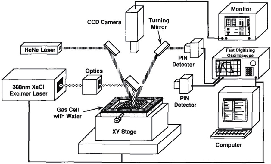
In 1986, Careyet al.[21] first proposed gas immersion laser doping (GILD) technique to fabricate As-hyperdoped Si. Afterwards, they obtained B-hyperdoped Si using the same method[55]. The laser doping apparatus is shown inFig. 1, which mainly consists of five components: a XeCI ns-pulsed excimer laser, an optical system, a gas cell, a XY stage and a computer. Hoummadaet al.[56] adopted atom probe tomography to analyze the 3D compositional profile of B-hyperdoped Si obtained by GILD. The results revealed that the concentration of the incorporated B was well above the solubility (6 × 1020 cm–3). No B clusters or precipitates were formed. In 2014, Sheret al.[57] fabricated S-hyperdoped Si using fs-pulsed laser GILD at different SF6 pressures. After optical-pump/terahertz-probe measurements, they found that the carrier lifetime decreased with increasing dopant concentration[58]. Then, they proposed that dopant profile and incorporation depth can be tuned by varying the precursor gas pressure and laser pulse parameters[59,60]. Donget al.[61] prepared N-hyperdoped Si using fs-pulsed laser GILD in NF3 atmosphere in 2014, and the SIMS result showed that the N concentration stabilized around 3.5 × 10¹⁹ atom/cm3, which was far exceed the solubility of N atoms in Si (4.5 × 1015 cm–3)[62]. Then in 2018 they designed N, Se and N, S co-hyperdoped Si using first-principles calculations, with the expectation that the hyperdoped Si would be effectively applied to achieve high-efficiency photovoltaic cells[63,64]. Concentration gradient usually exists in S-hyperdoped Si fabricated by fs-pulsed laser, leading to undesirable inhomogeneous material properties. Therefore, Linet al.[65] designed a manufacturing method with varying laser pulses and sulfur concentrations to prepare S-hyperdoped Si with a uniform concentration depth profile. Due to the development of thin film deposition technology, substantial researches on laser doping of thin film precursors have been reported in recent years[66-68]. The equipment for laser doping of thin film is simpler compared to GILD. Sheret al.[17] first deposited 65 nm Se or Te film on the surface of Si wafer through vacuum thermal evaporation technique, and then obtained Se- or Te-hyperdoped Si by fs-pulsed laser doping. Analogously, Yuet al.[69] and Qiuet al.[70] prepared Au- and Ag-hyperdoped Si by vacuum thermal evaporation combined with fs-pulsed laser doping.
![Schematic of laser doping apparatus and the main doping related components: (i) 308 nm XeC1 pulsed excimer laser, (ii) homogenizing optics, (iii)x–y stage and gas cell, and (iv) SUN workstation. Also shown are the diagnostic related components: (i) HeNe laser, (ii) CCD camera and monitor, (iii) PIN photodetectors, and (iv) fast digitizing oscilloscope. Reproduced with permission from Ref. [55]. Copyright Elsevier 1989.](/Images/icon/loading.gif)
Figure 1.Schematic of laser doping apparatus and the main doping related components: (i) 308 nm XeC1 pulsed excimer laser, (ii) homogenizing optics, (iii)x–y stage and gas cell, and (iv) SUN workstation. Also shown are the diagnostic related components: (i) HeNe laser, (ii) CCD camera and monitor, (iii) PIN photodetectors, and (iv) fast digitizing oscilloscope. Reproduced with permission from Ref. [55]. Copyright Elsevier 1989.
Others
Batalovet al.[71] used recoil-atom implantation method to fabricate Fe-hyperdoped Si, which utilized Xe+ ion beam to knock out Fe atoms from target to achieve incorporation of Fe into Si. The SIMS results showed that the utmost Fe concentration reached 1.7 × 1022 cm–3 (4 nm depth), which was well beyond the equilibrium solubility of Fe in Si (3 × 1016 cm–3 at 1300 °C). Chenet al.[72] successfully fabricated Ni-hyperdoped Si by linear type continuous-wave laser irradiation on Ni film deposited on Si wafer. The maximum Ni concentration of 1020 cm–3 had exceeded its solubility in Si[73].
In addition to bulk Si, the hyperdoping of Si nanocrystals and nanowires has also been investigated. For example, Luanet al.[74] synthesized B- and P-hyperdoped Si nanocrystals through nonthermal plasma. They then fabricated bulk Si with the resistivity of 0.8 mΩ·cm through hot pressing hyperdoped Si nanocrystals. Chenet al.[75] fabricated B-hyperdoped Si nanoparticles with B concentrations of 15, 25 and 42 at% through laser pyrolysis of SiH4 and B2H6. Moutanabbiret al.[76] synthesized Al-hyperdoped Si nanowires in an ultrahigh-vacuum chemical deposition system. The Al particles served as energetically favored sites for SiH4 adsorption and nucleation sites for one-dimensional growth.
Electronic and optical properties
Bulk Si
The radiative emission of Er3+ is around the wavelength of 1.54µm, which can be used for long-distance optical fiber telecommunication[77]. Therefore, doping Si with Er3+ is considered as a promising approach to produce Si-based light-emitting devices[78]. Wenet al.[79] fabricated Er/O hyperdoped Si by DC process, which exhibitd a strong photoluminescence at 1536 nm (Fig. 2(b)). Compared to RTA sample, the decay time of Er/O hyperdoped Si remained nearly constant (Fig. 2(c)).
Figure 2.(Color online) (a) Temperature-dependent PL spectra: Temperature-dependent peak amplitude at 1536 nm for DC- and RTA-processed Er/O-Si samples. Inset: the temperature-dependence of PL spectra for DC-processed samples. (b) Room-temperature PL spectra for DC-and RTA-processed samples. (c) Fast and slow decay times as a function of temperature for DC- and RTA-processed samples. Reproduced with permission from Ref. [79]. Copyright Wiley-VCH 2020.
Bustarretet al.[80] reported that B-hyperdoped Si achieved by GILD was a superconductor when the temperature was below 0.35 K and the critical field was about 0.4 T. According to Bardeen-Cooper-Schrieffer theory, electrons in the lattice attract positive charges at neighboring lattice points, forming a localized region of high positive charge to attract electrons with opposite spin. Electrons with opposite spin and momentum can form Cooper pairs, which can move in the lattice to generate superconducting currents[81]. Furthermore, ab initio calculations and Raman results indicated that B atoms were in substitutional sites. As shown inFig. 3, deep-level impurity band and sub-bandgaps were generated in Si hyperdoped with deep-level impurities[82-84]. Compared with chalcogen elements, transition-metal elements are more electroactive. Their impurity bands are closer to the center of intrinsic Si bandgap, which contributes to the decrease of the dark current and improves the sub-bandgap photoresponse[85-88]. The delocalization of impurity-band electrons leads to high conductivity and significant broadband infrared light absorption[89]. Zhouet al.[90] prepared Co-hyperdoped Si by ion implantation followed with PLA, and deduced from resistance-temperature curves that the fitting location of intermediate band was at 0.49–0.51 eV below the conduction band edge of Si. The maximum Co concentration could almost reach 1022 cm–3, far exceeding the solubility of Co in Si (below 1017 cm–3)[91]. The Co-hyperdoped Si with intermediate band could be a potential candidate in the field of photovoltaic devices, which was confirmed by simulations and calculations of Donget al.[92,93]. The high absorption coefficient of Ti-hyperdoped Si fabricated by Oleaet al.[94] could reach between 4 × 10³ and 104 cm–1. Tullet al.[95] found that the infrared absorptance of chalcogens (S, Se, and Te)-hyperdoped Si decreased with increasing annealing time (Fig. 4(a)) and the reduction was associated with a characteristic dopant diffusion length (Fig. 4(b)). Therefore, they proposed a simple diffusion model to explain that the diffusion of dopants and the precipitation at the grain boundarieswere the reasons of the decrease in infrared absorptance. After that, Newmanet al.[96] proposed that annealing at 1350–1550 K followed by rapid cooling (>50 K/s) or fs-pulsed laser treatment contributed to reactivation of sub-bandgap absorptance, as can be seen inFig. 4(c).
Figure 3.(Color online) Schematic illustration of sub-bandgap charge carrier excitation in deep-level impurity band (intermediate band) of hyperdoped Si.
Figure 4.(Color online) (a) Absorptance spectra for S-, Se-, and Te-hyperdoped Si after annealing to 775 K for increasing lengths of time (from top to bottom: 10 min, 30 min, 100 min, 6 h, 24 h). (b) Normalized absorptance for S- (circles), Se- (squares), and Te- (triangles) hyperdoped Si after various thermal anneals versus diffusion length of the respective dopant. Reproduced with permission from Ref. [95]. Copyright Springer-Verlag 2009. (c) Schematic of the two-step annealing process that first deactivates the sub-bandgap absorptance by annealing at 1070 K and then reactivates it via one of two methods: high temperature 1510 K annealing and quenching or fs-pulsed laser irradiation. Reproduced with permission from Ref. [96]. Copyright AIP Publishing 2011.
Wenet al.[97] evaluated the effects of annealing on morphology and optoelectronic properties of S-hyperdoped Si. As can be seen inFig. 5(a), conical structure arrays with small protrusions on the surface were obtained after ns-pulsed laser processing, resulting in additional reflection of visible light. The reflectance (400–1000 nm) decreased after annealing owing to the decreasing number of protrusions (Fig. 5(b)). Moreover, the infrared absorptance (1100–2400 nm) increased after annealing at 575 K and decreased as the temperature further increased (Fig. 5(c)) due to the precipitation of S dopants. Wanget al.[98] reported a novel S-hyperdoped Si prepared by surface texturing combined with ion implantation and PLA.Fig. 5(d) displayed the morphology of Si wafer surface after surface chemical texturing using alkaline solutions. After PLA, the pyramid structures changed into dome structures(Fig. 5(e)), which prolonged the effective path of incident light to increase the infrared absorptance from 30% to 70% (Fig. 5(f)).
Figure 5.(Color online) (a) Side-view SEM image of the S-hyperdoped Si sample prepared using ns-laser pulses. (b) Light reflection spectra of ns-laser-fabricated S-hyperdoped Si samples before and after the thermal annealing. The top insets A and B are schematic diagrams, which illustrate the optical path of light incident on the surface of conical structures before and after the thermal annealing. (c) Light absorption spectra of the ns-laser-fabricated S-hyperdoped Si samples before and after the thermal annealing (different S-dopant diffusion lengths). Reproduced with permission from Ref. [97]. Copyright Elsevier 2017. SEM images of the Si (001) wafer surface (d) after chemical texturing and (e) after laser melting. (f) Absorptance spectra of the non-textured and textured hyperdoped silicon samples, along with the pristine silicon wafer. Reproduced with permission from Ref. [98]. Copyright Springer Nature 2015.
Si nanocrystals
Hyperdoped Si nanocrystals give rise to LSPR in infrared spectral range due to large free carrier concentrations. As can be seen inFig. 6(a), with the increase of the doping level of B, an impurity band forms close to the valence band and expands. Moreover, the conduction band expands and the valence band edge moves downward[99]. After the ionized B concentration exceeded 1.8 × 1020 cm–3, band gap started narrowing (Fig. 6(b))[100]. The free holes from the impurity band will oscillate collectively under external excitation, which leads to remarkable light absorption[14,15,101]. Niet al.[102] found that the LSPR of B-hyperdoped Si nanocrystals could be tuned by not only the nanocrystals size but also the doping level. When the size decreased or doping level increased, the LSPR induced absorption blueshifted(Figs. 7(a) and7(b)). Rohaniet al.[103] synthesized B-hyperdoped Si nanocrystals with an average size of 25 nm through laser pyrolysis. The LSPR peak shifted toward higher frequencies as more B was incorporated into Si nanocrystals, which was consistent with the results of Niet al. Moreover, they found the LSPR peak disappeared after annealing at 800 °C due to B segregation (Fig. 7(c)). The outstanding air stability of B-hyperdoped Si nanocrystals shown inFig. 7(d) is advantageous for plasmonic devices.
Figure 6.(Color online) (a) Evolution of the Si nanocrystals band structure with the increase of the doping level of B. ABS: absorption onset;Ec: conduction band edge;Ev: valence band edge;Ef: Fermi energy level;Ea: impurity energy level. (b) Bandgap narrowing associated with the indirect transition (T0) and direct transition (T1) obtained in heavily B-doped Si nanocrystals. Reproduced with permission from Ref. [99]. Copyright American Chemical Society 2016.
Figure 7.(Color online) (a) FTIR spectra of ~6.8 nm undoped and B-hyperdoped Si nanocrystals. (b) FTIR spectra of ~2.4, 3.8, and 6.8 nm B-hyperdoped Si nanocrystals with the B concentration of ~17%. (c) The peak positions of the LSPR-induced absorption that is fitted with dashed lines are indicated by dotted lines. Reproduced with permission from Ref. [102]. Copyright Wiley-VCH 2016. FTIR spectra of 14.6 at% B-hyperdoped Si nanocrystals with 600, 700, and 800 °C annealing temperatures. (d) FTIR spectra of the as-synthesized (solid lines) and one-year air-exposed (dashed lines) undoped and B-hyperdoped Si nanocrystals. Reproduced with permission from Ref. [103]. Copyright Wiley-VCH 2019.
Si nanowires
Compared with bulk Si, nanostructured Si like Si nanowires with a larger specific surface area can be used in nanoelectronics as building blocks to overcome the Schottky limit[104-108]. Berencenet al.[109] reported Se-hyperdoped Si nanowires with specific resistivity of 1.27 Ω·cm and sub-bandgap optoelectronic photoresponse. The Si nanowires were fabricated by vapor-liquid-solid method. The hyperdoping of Se was achieved through ion implantation and FLA. Moutanabbiret al.[76] successfully synthesized Al-hyperdoped Si nanowires using Al-Si nanoparticles as the energetically favored sites for SiH4 and the nucleation sites for one-dimensional growth. From the concentration profiles of Al, they found that Al was homogeneously distributed in the Al-hyperdoped Si nanowire. The average Al concentration of ~(2.0 ± 0.5) × 1020 cm–3 was about four orders of magnitude greater than the equilibrium solubility of Al in Si[110]. Changet al.[111] adopted supercritical fluid-liquid-solid method to obtain P-hyperdoped Si nanowires. It is worth mentioning that they used red P nanoparticles rather than toxic PH3[112]. It can be seen inFig. 8 that the P concentration was as high as 2 at% in Si nanowires. The resistivity of P-hyperdoped Si nanowires was 4.3 × 10⁻³ Ω·m.
Figure 8.(Color online) (a) TEM image and (b, c) EDS element mapping of P-hyperdoped Si nanowires. (d) Two-probeI–V measurements of P-hyperdoped Si nanowires and intrinsic Si nanowires for comparison. Reproduced with permission from Ref. [111]. Copyright American Chemical Society 2021.
Si films
Dimensionally constrained Si films can control phonon transmittance and reduce Si thermal conductivity, which allows them to find application niches in the field of microelectronics like flexible solar cells[113-116]. Wanget al.[117] prepared Ti-hyperdoped Si nanofilms through the method of magnetron sputtering combined with PLA. Three layers were deposited alternately on a Si substrate to form a sandwich structure, as shown inFig. 9(a). Unlike SIMS results of other hyperdoped Si, the Ti atom distribution was homogeneous (Fig. 9(b)) and the average Ti concentration could reach 5 × 1020 cm–3 (far exceeding the solubility of Ti in Si)[118]. It can be seen inFig. 9(c) that the maximum light absorption coefficient of Ti-hyperdoped Si sample was about 1.2 × 104 cm–1, which was much higher than that of Si and the sample without PLA. Wenet al.[119] prepared Si–S–Si multilayered films (Fig. 10(a)) through film deposition and ns-pulsed laser doping. The multilayered structure was confirmed by TEM (Fig. 10(b)). As can be seen inFigs. 10(c)–10(f), the maximum absorptance, sheet carrier concentration and Hall mobility of S-hyperdoped Si samples were 90%, 1.139 × 10¹⁵ electrons/cm2 and 72.29 cm2/(V·s), respectively. Furthermore, the samples exhibited high near-infrared light absorptance (75%–90%) and low sheet resistance (75.8 Ω/□).
Figure 9.(a) The sketch of the structure of Si–Ti–Si. (b) Atom concentration and the atom percentage of Ti in sample after PLM. (c) Light absorption coefficient of the thin film wafer of samples and Si. Reproduced with permission from Ref. [117]. Copyright Science Press 2018.
Figure 10.(Color online) (a) Sample geometry of Si–S–Si multilayered films. (b) TEM bright-field images of Si–S–Si multilayered films after ns-pulsed laser irradiation with fluences of 175 mJ/cm2. (c) Absorptance profiles of the S-hyperdoped Si samples and the substrate, temperature characteristics of (d) sheet carrier concentration, (e) Hall mobility and (f)sheet resistance for the S-hyperdoped Si samples and the substrate. Reproduced with permission from Ref. [119]. Copyright Elsevier 2019.
Device applications
Hyperdoped Si obtained by non-equilibrium doping methods such as ion implantation and laser doping not only can be used in novel infrared photodetectors and intermediate band solar cells[120-122], but also holds promise for the development of superconductors[123], cryogenic circuit[124], gas sensor[125] and light-emitting diodes[79]. At present, most of the hyperdoped Si devices are based on bulk Si. Extensive theoretical calculations about band structure engineering and optoelectronic properties have also been carried out, which provide theoretical guidance for future applications of hyperdoped Si[126-128].
Qiuet al.[129] reported a Ag-hyperdoped Si-based photodetector with responsivities of 504 mA/W at 1310 nm and 65 mA/W at 1550 nm under –3 V bias. The enhanced photoresponse was induced by the deep-level electron traps and two-stage carrier excitation. The Er/O hyperdoped Si wafers prepared by Zhaoet al.[26] were further doped with B to fabricate photodiodes, which exhibited significant photoresponsivity (up to 100 mA/W) at the communication wavelength of 1510 nm. In additon, the 3 dB bandwidth of the Er/O hyperdoped Si waveguide photodiode reached 30 kHz. Batalovet al.[71] prepared Fe-hyperdoped Si layers on p-type Si wafer by recoil-atom implantation. The schematic representation of the doping process and the HRTEM image of Si:Fe/p-Si structure can be observed inFigs. 11(a) and11(b). The darkI–V characteristics inFig. 11(c) displayed diode behavior of the hyperdoped sample compared with the ohmic behavior of p-Si substrate.Fig. 11(d) shows the photoresponse of the Si:Fe/p-Si sample under different reverse bias (0–1.6 V). It can be observed that the photoresponse of the sample under –1.0 V bias is close to that of a commercial Si photodiode (FD-27K).
Figure 11.(Color online) (a) Schematic representation of the recoil-Fe atom implantation method. (b) HRTEM image of the (110) cross section of the Si:Fe/p-Si structure. (c) DarkI–V characteristics of the p-Si substrate and the n-Si:Fe/p-Si diode structure and (d) photoresponse of the n-Si:Fe/p-Si sample at various values of the reverse bias (U = 0–1.6 V) and the commercial silicon photodiode FD-27K at the reverse biasU = 10 V. Reproduced with permission from Ref. [71]. Copyright Elsevier 2020.
Table Infomation Is Not Enable
It is reported that a N-hyperdoped Si photodiode fabricated exhibited a photoresponsivity of 5.3 mA/W at 1.31µm and good thermal stability[130]. The double-absorbing-layer photodiode displayed a higher responsivity compared with single-absorbing-layer photodiode. Wanget al.[131] proposed an etching treatment (reactive ion etching based on SF6 plasma) to improve the photoresponse of a S-hyperdoped Si-based photodiode (Fig. 12(a)) working at 1064 nm. They investigated the effects of laser fluence and etching time on the photoresponse(Figs. 12(b) and12(c)). The photoresponse degradation after laser fluence above 0.2 J/cm2 was ascribed to the reduction in carrier lifetime and carrier mobility induced by substantial structure defects and recombination sites[132]. It is worth mentioning that the photoresponsivity could be improved to 0.45 A/W by controlling the etching time.
Figure 12.(Color online) (a) Cross-sectional structure of Si-photodiode based on microstructured Si. (b) Responsivity versus laser fluence at –5 V bias. (c) Responsivity versus etching time at –5 V bias. Reproduced with permission from Ref. [131]. Copyright IOP Publishing 2018.
García-Hemmeet al.[133] fabricated infrared photodetectors based on Ti-hyperdoped Si. The high sub-bandgap responsivity of 34 mV/W and specific detectivity of 1.7 × 104 cm·Hz1/2/W (660 Hz) were obtained at the wavelength of 1.55µm. A Te-hyperdoped Si photodiode prepared by Wanget al. exhibited the maximum room-temperature specific detectivity of 3.2 × 10¹² (9.2 × 10⁸) cm· Hz1/2/W at 1.0 (1.55)µm, which was comparable to that of the commercial devices[134,135]. As shown inFig. 13(a), the room-temperature responsivity of 79 (0.3) mA/W was obtained at 1.12 (1.55)μm. As the temperature decreased, the photoresponse range expanded to the mid-wavelength infrared range (Figs. 13(a)–13(g)). In the temperature range of 20–26 K, the wavelength with photoresponse was extended to 5μm. The sub-bandgap photoresponse mechanism of the Te-hyperdoped Si photodetector was depicted inFig. 13(h).
Figure 13.(Color online) (a–g) The spectral responsivity measured at zero bias (i.e., photovoltaic mode) for the Te-hyperdoped Si photodetector at different temperatures. (h) Brown short dot is the room-temperature spectral responsivity of a commercial Si-PIN photodiode (model: BPW34). Illustration of the below-bandgap photoresponse in the Te-hyperdoped Si photodetector. Process I: valence band to conduction band (Eph ≥ Eg); Process II: valence band to intermediate band (Eph ≥Eg –ETe); Process III: intermediate band to conduction band (Eph ≥ETe, only measurable at low temperatures where the thermal contribution is neglected). Reproduced with permission from Ref. [135]. Copyright Wiley-VCH 2021.
As another example, a photodetector based on Te-hyperdoped Si showed superior performance[67]. The maximum Te concentration in the hyperdoped Si was 1.2 × 1020 cm–3, which was far beyond the solubility of Te in Si (3.5 × 1016 cm–3)[136]. The maximum responsivity of 120.6 A/W was obtained at 1120 nm. Moreover, the responsivity at 1550 nm was 56.8 mA/W with low noise. Mailoaet al.[27] fabricated a Au-hyperdoped Si photodiode (Fig. 14(a)) with the largest Au concentration up to 5 × 1020 cm–3, which was above the solubility of Au in Si (<1015 cm–3)[137]. As shown inFig. 14(c), carrier drift velocity in the Si:Au layer increased as the reverse bias on the junction increased, promoting the gathering of carriers excited by the sub-bandgap light. Mapped external quantum efficiency (EQE) confirmed that sub-bandgap response was attributed to Si:Au layer, while no sub-bandgap response was observed in the reference photodiode. The EQE for three different sub-bandgap wavelengths (1310, 1550 and 1650 nm) increased with the increase of the Au concentration (Fig. 14(f)). The Ni-hyperdoped Si photodiode first reported by Chenet al.[72] exhibited a remarkable photoresponse of 0.15–0.18 V/W in the wavelength range of 1200–1750 nm. The performance of photodetectors based on hyperdoped Si is summarized inTable 1.
Figure 14.(Color online) (a) Au-hyperdoped Si-based photodiode with Si:Au layer on n-Si substrate operating at reverse bias. (b) DarkI–V curves of three different Au implantation doses. (c) Difference between dark and illuminatedI–V of the photodiode with 1015 cm–2 Au dose. (d) Mapped EQE of Si:Au layer for 1550 nm. (e) Mapped EQE of Si reference for 1550 nm. (f) EQE of Au-hyperdoped Si-based photodiode for three different sub-band gap wavelengths. Reproduced with permission from Ref. [27]. Copyright nature publishing group 2014.
Hyperdoped Si may be also used for intermediate band solar cells[138]. Fs laser doping can simultaneously obtain hyperdoping and surface texturing, which has been employed for solar cell fabrication[139]. Wenet al.[119] designed a novel structure in which S-hyperdoped Si layer was grown on the front surface of a commercial Si solar cell substrate. Compared to the back-surface structure, the front-surface structure (Fig. 15) increased photocurrent for near-infrared and visible light. Moreover, the carrier recombination loss was reduced due to the narrow transport distance of photogenerated carriers to the PN junction. Gimpelet al.[140] compared the effect of different metal layer systems and deposition techniques on the contact behavior of devices based on S-hyperdoped Si.I–V curves and reactance spectra results showed that pulsed laser deposition Ti/Pd/Ag was the most promising front contact for solar cells. After exploring the temperature dependence of absorption and quantum efficiency for S-hyperdoped Si solar cells, they found that annealing enhanced the photoelectrical conversion below Si bandgap, which was important for the development of multijunction solar cells[141].
Figure 15.(Color online) Schematic cross-section of Si-based solar cell structures. S-hyperdoped Si layer directly grown on the (a) back surface and (b) front surface of solar cell. Reproduced with permission from Ref. [119]. Copyright Elsevier 2019.
As mentioned above, GILD can help realize B-hyperdoped Si with superconductivity[142]. Grockowiaket al.[143,144] fabricated a series of B-hyperdoped Si through GILD with B concentrations varying between ~3 × 10²⁰ to ~6 × 1021 cm–3. They concluded that critical temperature was entirely determined by the B concentration. Chiodiet al.[123] observed a reduction of contact resistance to 0 Ω as the B concentration exceeded 1020 cm–3 for a bilayer-based superconductor junction, as shown inFig. 16(a). Furthermore, they measured resistance of the superconductor junction at low temperature. It was found that the junction was superconducting at 215 mK (Fig. 16(b)), which was higher than the critical temperature (~160 mK) for normal metals. The voltage–current characteristic of the junction at 80 mK (the inset of Fig. 16(b)) indicated that the critical current for the transition from superconducting to ohmic state was 2.6µA, while the retrapping current at which the junction switched back to superconducting state was 1.0µA. Fs laser hyperdoped Si can be used for gas sensors due to its advantages of abundant surface states and unique surface morphology[145,146]. A NO2 gas sensor[147] was fabricated by using N-hyperdoped Si (Fig. 17(a)), exhibiting outstanding performance including high response and good selectivity. The average response, response and recovery time for 20 ppm NO2 were about 79.34%, 12 s and 36 s, respectively (Figs. 17(b) and17(c)).
Figure 16.(Color online) (a) Deduced contact resistance vs. B doping concentration. (b) Resistance vs. temperature for a superconductor junction. The bias lock-in current is 5 nA. The contacts transition temperature can be seen at 215 mK, while the weak link transits is at a lower temperature (~160 mK). On the right, schematics of the resistance jumps origin. Inset: current-voltage characteristic atT = 80 mK. Reproduced with permission from Ref. [123]. Copyright Elsevier 2014.
Figure 17.(Color online) (a) Schematic illustration of the gas sensor. (b) Gas responses to various gases or volatile organic compound vapors and (c) response time and recovery time of the gas sensor upon the exposure to 20 ppm NO2 gas with different storage days. Reproduced with permission from Ref. [147]. Copyright Elsevier 2022.
Summary and perspectives
Hyperdoping methods such as ion-implantation with subsequent heat treatment and laser doping have been employed to tune the properties of Si, which are compatible with the processing of Si materials and devices. Novel properties like superconductivity and near-infrared photoresponse have been enabled by using hyperdoping for Si, which may be in the form of bulk Si, Si films, Si nanowires or Si nanocrystals. Hyperdoped Si has been used to fabricate devices such as infrared photodetectors and solar cells.
Surface texturing induced by laser irradiation is advantageous for the enhancement of infrared absorption. Further investigation on this aspect may lead to infrared photodetectors with improved performance. Hyperdoping has made Si be a plasmonic material. The plasmonic properties of all kinds of Si deserve careful investigation. The effect of the hyperdoping processes on the performance of devices based on hyperdoped Si needs to be studied to facilitate novel device design. It is clear that the research on the hyperdoping of Si should inspire work on hyperdoping other semiconductors and exploring their use in all types of devices.
Acknowledgements
This work was supported by the National Key Research and Development Program of China (Grant Nos. 2017YFA0205704 and 2018YFB2200101) and the Natural Science Foundation of China (Grant Nos. 91964107 and U20A20209). Partial support was provided by the Natural Science Foundation of China for Innovative Research Groups (Grant No. 61721005).
References
[1] C B Simmons, A J Akey, J P Mailoa et al. Enhancing the infrared photoresponse of silicon by controlling the fermi level location within an impurity band. Adv Funct Mater, 24, 2852(2014).
[2] X D Pi. Doping silicon nanocrystals with boron and phosphorus. J Nanomater, 2012, 3(2012).
[3] I Marri, E Degoli, S Ossicini. Doped and codoped silicon nanocrystals: The role of surfaces and interfaces. Prog Surface Sci, 92, 375(2017).
[4] M Wang, A Debernardi, Y Berencén et al. Breaking the doping limit in silicon by deep impurities. Phys Rev Applied, 11, 054039(2019).
[5] K Sánchez, I Aguilera, P Palacios et al. Formation of a reliable intermediate band in Si heavily coimplanted with chalcogens (S, Se, Te) and group III elements (B, Al). Phys Rev B, 82, 165201(2010).
[6] F Liu, S Prucnal, Y Berencén et al. Realizing the insulator-to-metal transition in Se-hyperdoped Si via non-equilibrium material processing. J Phys D, 50, 415102(2017).
[7] J Olea, G González-Díaz, D Pastor et al. Electronic transport properties of Ti-impurity band in Si. J Phys D, 42, 085110(2009).
[8] P Dai, Y Zhang, M P Sarachik. Critical conductivity exponent for Si:B. Phys Rev Lett, 66, 1914(1991).
[9] K F Wang, H Z Shao, K Liu et al. Possible atomic structures responsible for the sub-bandgap absorption of chalcogen-hyperdoped silicon. Appl Phys Lett, 107, 112106(2015).
[10] E García-Hemme, R García-Hernansanz, J Olea et al. Far infrared photoconductivity in a silicon based material: Vanadium supersaturated silicon. Appl Phys Lett, 103, 032101(2013).
[11] G Haberfehlner, M J Smith, J C Idrobo et al. Selenium segregation in femtosecond-laser hyperdoped silicon revealed by electron tomography. Microsc Microanal, 19, 716(2013).
[12] A Luque, A Martí, E Antolín et al. Intermediate bands versus levels in non-radiative recombination. Phys B, 382, 320(2006).
[13] M Wang, R Hübner, C Xu et al. Thermal stability of Te-hyperdoped Si: Atomic-scale correlation of the structural, electrical, and optical properties. Phys Rev Mater, 3, 044606(2019).
[14] S Zhou, X D Pi, Z Y Ni et al. Boron- and phosphorus-hyperdoped silicon nanocrystals. Part Part Syst Charact, 32, 213(2015).
[15] D J Rowe, J S Jeong, K A Mkhoyan et al. Phosphorus-doped silicon nanocrystals exhibiting mid-infrared localized surface plasmon resonance. Nano Lett, 13, 1317(2013).
[16] K F Wang, S C Qu, D W Liu et al. Large enhancement of sub-band-gap light absorption of sulfur hyperdoped silicon by surface dome structures. Mater Lett, 107, 50(2013).
[17] M J Sher, Y T Lin, M T Winkler et al. Mid-infrared absorptance of silicon hyperdoped with chalcogen via fs-laser irradiation. J Appl Phys, 113, 063520(2013).
[18] C B Simmons, A J Akey, J J Krich et al. Deactivation of metastable single-crystal silicon hyperdoped with sulfur. J Appl Phys, 114, 243514(2013).
[19] W Yang, N Ferdous, P J Simpson et al. Evidence for vacancy trapping in Au-hyperdoped Si following pulsed laser melting. APL Mater, 7, 101124(2019).
[20] J M Bao, M Tabbal, T Kim et al. Point defect engineered Si sub-bandgap light-emitting diode. Opt Express, 15, 6727(2007).
[21] P G Carey, K Bezjian, T W Sigmon et al. Fabrication of submicrometer MOSFET's using gas immersion laser doping (GILD). IEEE Electron Device Lett, 7, 440(1986).
[22] C Wen, Z Q Shi, Z J Wang et al. Zinc-hyperdoped silicon nanocrystalline layers prepared via nanosecond laser melting for broad light absorption. Opt Laser Technol, 144, 107415(2021).
[23] F F Komarov, N S Nechaev, G D Ivlev et al. Structural and optical properties of Si hyperdoped with Te by ion implantation and pulsed laser annealing. Vacuum, 178, 109434(2020).
[24] L Eriksson, J A Davies, J W Mayer. Ion implantation studies in silicon. Science, 163, 627(1969).
[25] P G Kik, A Polman, S Libertino et al. Design and performance of an erbium-doped silicon waveguide detector operating at 1.5µm. J Light Technol, 20, 862(2002).
[26] X Y Zhao, K M Lin, S Gao et al. Efficient Er/O doped silicon photodiodes at communication wavelengths by deep cooling. Adv Mater Technol, 2100137(2021).
[27] J P Mailoa, A J Akey, C B Simmons et al. Room-temperature sub-band gap optoelectronic response of hyperdoped silicon. Nat Commun, 5, 1(2014).
[28] D Recht, J T Sullivan, R Reedy et al. Controlling dopant profiles in hyperdoped silicon by modifying dopant evaporation rates during pulsed laser melting. Appl Phys Lett, 100, 112112(2012).
[29] S J Li, P D Han. Effects of high temperature annealing and laser irradiation on activation rate of phosphorus. J Semicond, 41, 122701(2020).
[30] B P Bob, A Kohno, S Charnvanichborikarn et al. Fabrication and subband gap optical properties of silicon supersaturated with chalcogens by ion implantation and pulsed laser melting. J Appl Phys, 107, 123506(2010).
[31] W Yang, Q Hudspeth, P K Chow et al. Atomistic mechanisms for the thermal relaxation of Au-hyperdoped Si. Phys Rev Appl, 12, 024015(2019).
[32] S Q Lim, C T K Lew, P K Chow et al. Toward understanding and optimizing Au-hyperdoped Si infrared photodetectors. APL Mater, 8, 061109(2020).
[33] S Q Lim, A J Akey, E Napolitani et al. A critical evaluation of Ag- and Ti-hyperdoped Si for Si-based infrared light detection. J Appl Phys, 129, 065701(2021).
[34] S Prucnal, L Rebohle, W Skorupa. Doping by flash lamp annealing. Mater Sci Semicond Process, 62, 115(2017).
[35] Y Berencén, S Prucnal, F Liu et al. Room-temperature short-wavelength infrared Si photodetector. Sci Rep, 7, 43688(2017).
[36] R A McMahon, M P Smith, K A Seffen et al. Flash-lamp annealing of semiconductor materials—Applications and process models. Vacuum, 81, 1301(2007).
[37] S Q Zhou, F Liu, S Prucnal et al. Hyperdoping silicon with selenium: Solidvs. liquid phase epitaxy. Sci Rep, 5, 8329(2015).
[38] M Wang, Y Yu, S Prucnal et al. Mid- and far-infrared localized surface plasmon resonances in chalcogen-hyperdoped silicon. Nanoscale, 14, 2826(2022).
[39] K Wang, J S Gao, H G Yang et al. Study on top sulfur hyperdoping layer covering microstructured Si by fs-laser irradiation. Appl Surf Sci, 464, 502(2019).
[40] S H Pan, D Recht, S Charnvanichborikarn et al. Enhanced visible and near-infrared optical absorption in silicon supersaturated with chalcogens. Appl Phys Lett, 98, 121913(2011).
[41] H B Sun, X L Liu, L Zhao et al. Mid-long wavelength infrared absorptance of hyperdoped silicon via femtosecond laser microstructuring. Opt Express, 30, 1808(2022).
[42] M V Limaye, S C Chen, C Y Lee et al. Understanding of sub-band gap absorption of femtosecond-laser sulfur hyperdoped silicon using synchrotron-based techniques. Sci Rep, 5, 11466(2015).
[43] J E Carey, C H Crouch, M Y Shen et al. Visible and near-infrared responsivity of femtosecond-laser microstructured silicon photodiodes. Opt Lett, 30, 1773(2005).
[44] T Gimpel, I Höger, F Falk et al. Electron backscatter diffraction on femtosecond laser sulfur hyperdoped silicon. Appl Phys Lett, 101, 111911(2012).
[45] J M Warrender. Laser hyperdoping silicon for enhanced infrared optoelectronic properties. Appl Phys Rev, 3, 031104(2016).
[46] C H Crouch, J E Carey, M Shen et al. Infrared absorption by sulfur-doped silicon formed by femtosecond laser irradiation. Appl Phys A, 79, 1635(2004).
[47] M J Smith, Y T Lin, M J Sher et al. Pressure-induced phase transformations during femtosecond-laser doping of silicon. J Appl Phys, 110, 053524(2011).
[48] T Gimpel, K M Guenther, S Kontermann et al. Current-voltage characteristic and sheet resistances after annealing of femtosecond laser processed sulfur emitters for silicon solar cells. Appl Phys Lett, 105, 053504(2014).
[49] S K Sundaram, E Mazur. Inducing and probing non-thermal transitions in semiconductors using femtosecond laser pulses. Nat Mater, 1, 217(2002).
[50] C H Crouch, J E Carey, J M Warrender et al. Comparison of structure and properties of femtosecond and nanosecond laser-structured silicon. Appl Phys Lett, 84, 1850(2004).
[51] B Franta, D Pastor, H H Gandhi et al. Simultaneous high crystallinity and sub-bandgap optical absorptance in hyperdoped black silicon using nanosecond laser annealing. J Appl Phys, 118, 225303(2015).
[52] J Olea, M Toledano-Luque, D Pastor et al. High quality Ti-implanted Si layers above the Mott limit. J Appl Phys, 107, 103524(2010).
[53] I Umezu, M Naito, D Kawabe et al. Hyperdoping of silicon with deep-level impurities by pulsed YAG laser melting. Appl Phys A, 117, 155(2014).
[54] Y B Zhang, X H Li, X M Lin et al. Negative photoconductivity in sulfur-hyperdoped silicon film. Mater Sci Semicond Process, 98, 106(2019).
[55] P G Carey, T W Sigmon. In-situ doping of silicon using the gas immersion laser doping (GILD) process. Appl Surf Sci, 43, 325(1989).
[56] K Hoummada, F Dahlem, T Kociniewski et al. Absence of boron aggregates in superconducting silicon confirmed by atom probe tomography. Appl Phys Lett, 101, 182602(2012).
[57] M J Sher, E Mazur. Intermediate band conduction in femtosecond-laser hyperdoped silicon. Appl Phys Lett, 105, 032103(2014).
[58] M J Sher, C B Simmons, J J Krich et al. Picosecond carrier recombination dynamics in chalcogen-hyperdoped silicon. Appl Phys Lett, 105, 053905(2014).
[59] S Meng-Ju, N M Mangan, M J Smith et al. Femtosecond-laser hyperdoping silicon in an SF6 atmosphere: Dopant incorporation mechanism. J Appl Phys, 117, 125301(2015).
[60] R O Carlson, R N Hall, E M Pell. Sulfur in silicon. J Phys Chem Solids, 8, 81(1959).
[61] X Dong, N Li, Z Zhu et al. A nitrogen-hyperdoped silicon material formed by femtosecond laser irradiation. Appl Phys Lett, 104, 091907(2014).
[62] C R Alpass, J D Murphy, R J Falster et al. Nitrogen diffusion and interaction with dislocations in single-crystal silicon. J Appl Phys, 105, 013519(2009).
[63] X Dong, Y Y Wang, X H Song. Engineering intermediate-band photovoltaic material by heavily co-doping selenium and nitrogen in silicon. Appl Phys Express, 11, 011303(2018).
[64] X Dong, Y Y Wang, X H Song et al. First-principles studies of a photovoltaic material based on silicon heavily codoped with sulfur and nitrogen. Appl Phys Express, 11, 031303(2018).
[65] Y T Lin, N Mangan, S Marbach et al. Creating femtosecond-laser-hyperdoped silicon with a homogeneous doping profile. Appl Phys Lett, 106, 062105(2015).
[66] B K Newman, E Ertekin, J T Sullivan et al. Extended X-ray absorption fine structure spectroscopy of selenium-hyperdoped silicon. J Appl Phys, 114, 133507(2013).
[67] Z X Jia, Q Wu, X R Jin et al. Highly responsive tellurium-hyperdoped black silicon photodiode with single-crystalline and uniform surface microstructure. Opt Express, 28, 5239(2020).
[68] L Y Du, Z M Wu, R Li et al. Near-infrared photoresponse of femtosecond-laser processed Se-doped silicon n+-n photodiodes. Opt Lett, 41, 5031(2016).
[69] X Y Yu, J H Zhao, C H Li et al. Gold-hyperdoped black silicon with high IR absorption by femtosecond laser irradiation. IEEE Trans Nanotechnol, 16, 502(2017).
[70] X D Qiu, X G Yu, S Yuan et al. Trap assisted bulk silicon photodetector with high photoconductive gain, low noise, and fast response by Ag hyperdoping. Adv Opt Mater, 6, 1700638(2018).
[71] R Batalov, R Bayazitov, I Faizrakhmanov et al. Photoelectric and magnetic properties of Fe-hyperdoped Si layers formed by the recoil-atom implantation. Mater Sci Semicond Process, 105, 104752(2020).
[72] R Chen, B D Fan, M Pan et al. Room-temperature optoelectronic response of Ni supersaturated p-type Si processed by continuous-wave laser irradiation. Mater Lett, 163, 90(2016).
[73] A A Istratov, P Zhang, R J McDonald et al. Nickel solubility in intrinsic and doped silicon. J Appl Phys, 97, 023505(2005).
[74] Q B Luan, Z Y Ni, S Koura et al. Low-resistivity bulk silicon prepared by hot-pressing boron- and phosphorus-hyperdoped silicon nanocrystals. AIP Adv, 4, 127108(2014).
[75] J J Chen, P Rohani, S G Karakalos et al. Boron-hyperdoped silicon for the selective oxidative dehydrogenation of propane to propylene. Chem Commun, 56, 9882(2020).
[76] O Moutanabbir, D Isheim, H Blumtritt et al. Colossal injection of catalyst atoms into silicon nanowires. Nature, 496, 78(2013).
[77] Z P Zhou, B Yin, J Michel. On-chip light sources for silicon photonics. Light Sci Appl, 4, e358(2015).
[78] A Polman. Erbium implanted thin film photonic materials. J Appl Phys, 82, 1(1997).
[79] H M Wen, J J He, J Hong et al. Efficient Er/O-doped silicon light-emitting diodes at communication wavelength by deep cooling. Adv Opt Mater, 8, 2000720(2020).
[80] E Bustarret, C Marcenat, P Achatz et al. Superconductivity in doped cubic silicon. Nature, 444, 465(2006).
[81] L Boeri, J Kortus, O K Andersen. Three-dimensional MgB2-type superconductivity in hole-doped diamond. Phys Rev Lett, 93, 237002(2004).
[82] E Ertekin, M T Winkler, D Recht et al. Insulator-to-metal transition in selenium-hyperdoped silicon: Observation and origin. Phys Rev Lett, 108, 026401(2012).
[83] W J Yang, J Mathews, J S Williams. Hyperdoping of Si by ion implantation and pulsed laser melting. Mater Sci Semicond Process, 62, 103(2017).
[84] J T Sullivan, C B Simmons, J J Krich et al. Methodology for vetting heavily doped semiconductors for intermediate band photovoltaics: A case study in sulfur-hyperdoped silicon. J Appl Phys, 114, 103701(2013).
[85] M A Sheehy, B R Tull, C M Friend et al. Chalcogen doping of silicon via intense femtosecond-laser irradiation. Mater Sci Eng B, 137, 289(2007).
[86] D Recht, D Hutchinson, T Cruson et al. Contactless microwave measurements of photoconductivity in silicon hyperdoped with chalcogens. Appl Phys Express, 5, 041301(2012).
[87] J J Krich, B I Halperin, A Aspuru-Guzik. Nonradiative lifetimes in intermediate band photovoltaics—Absence of lifetime recovery. J Appl Phys, 112, 013707(2012).
[88] J T Sullivan, C B Simmons, T Buonassisi et al. Targeted search for effective intermediate band solar cell materials. IEEE J Photovolt, 5, 212(2015).
[89] X Y Li, P D Han, L P Gao et al. Electronic properties investigation of silicon supersaturated with tellurium. Appl Phys A, 105, 1021(2011).
[90] Y R Zhou, F Z Liu, X H Song. The insulator-to-metal transition of Co hyperdoped crystalline silicon. J Appl Phys, 113, 103702(2013).
[91] E R Weber. Transition metals in silicon. Appl Phys A, 30, 1(1983).
[92] X Dong, X X Fang, Y Y Wang et al. Modulating the band structure and sub-bandgap absorption of Co-hyperdoped silicon by co-doping with shallow-level elements. Appl Phys Express, 11, 061301(2018).
[93] X Dong, X H Song, Y Y Wang et al. First-principles calculations of a promising intermediate-band photovoltaic material based on Co-hyperdoped crystalline silicon. Appl Phys Express, 8, 081302(2015).
[94] J Olea, A del Prado, D Pastor et al. Sub-bandgap absorption in Ti implanted Si over the Mott limit. J Appl Phys, 109, 113541(2011).
[95] B R Tull, M T Winkler, E Mazur. The role of diffusion in broadband infrared absorption in chalcogen-doped silicon. Appl Phys A, 96, 327(2009).
[96] B K Newman, M J Sher, E Mazur et al. Reactivation of sub-bandgap absorption in chalcogen-hyperdoped silicon. Appl Phys Lett, 98, 251905(2011).
[97] C Wen, W Chen, Y P Chen et al. Thermal annealing performance of sulfur-hyperdoped black silicon fabricated using a Nd: YAG nanosecond-pulsed laser. Mater Res Bull, 93, 238(2017).
[98] K F Wang, P G Liu, S C Qu et al. Optical and electrical properties of textured sulfur-hyperdoped silicon: A thermal annealing study. J Mater Sci, 50, 3391(2015).
[99] S Zhou, Z Y Ni, Y Ding et al. Ligand-free, colloidal, and plasmonic silicon nanocrystals heavily doped with boron. ACS Photonics, 3, 415(2016).
[100] J W Slotboom, H C de Graaff. Measurements of bandgap narrowing in Si bipolar transistors. Solid State Electron, 19, 857(1976).
[101] X D Pi, C Delerue. Tight-binding calculations of the optical response of optimally P-doped Si nanocrystals: A model for localized surface plasmon resonance. Phys Rev Lett, 111, 177402(2013).
[102] Z Y Ni, X D Pi, S Zhou et al. Size-dependent structures and optical absorption of boron-hyperdoped silicon nanocrystals. Adv Opt Mater, 4, 700(2016).
[103] P Rohani, S Banerjee, S Sharifi-Asl et al. Synthesis and properties of plasmonic boron-hyperdoped silicon nanoparticles. Adv Funct Mater, 29, 1807788(2019).
[104] M C Beard, J M Luther, A J Nozik. The promise and challenge of nanostructured solar cells. Nat Nanotechnol, 9, 951(2014).
[105] Y Cui, C M Lieber. Functional nanoscale electronic devices assembled using silicon nanowire building blocks. Science, 291, 851(2001).
[106] B Z Tian, X L Zheng, T J Kempa et al. Coaxial silicon nanowires as solar cells and nanoelectronic power sources. Nature, 449, 885(2007).
[107] H Zhou, H Wang, L M Ding. Perovskite nanowire networks for photodetectors. J Semicond, 42, 110202(2021).
[108] L Y Li, Y F Cheng, Z Y Liu et al. Study of structure-property relationship of semiconductor nanomaterials by off-axis electron holography. J Semicond, 43, 041103(2022).
[109] Y Berencén, S Prucnal, W Möller et al. CMOS-compatible controlled hyperdoping of silicon nanowires. Adv Mater Interfaces, 5, 1800101(2018).
[110] Y Ke, X J Weng, J M Redwing et al. Fabrication and electrical properties of si nanowires synthesized by Al catalyzed vapor-liquid-solid growth. Nano Lett, 9, 4494(2009).
[111] C B Chang, C Y Tsai, K T Chen et al. Solution-grown phosphorus-hyperdoped silicon nanowires/carbon nanotube bilayer fabric as a high-performance lithium-ion battery anode. ACS Appl Energy Mater, 4, 3160(2021).
[112] Y Tanaka, M Furata, H Mastuura et al. Development of high-sensitive gas-sensor for B2H6 using gas-permeable conductive DLC membrane. ECS Trans, 16, 387(2008).
[113] D Narducci, L Zulian, B Lorenzi et al. Exceptional thermoelectric power factors in hyperdoped, fully dehydrogenated nanocrystalline silicon thin films. Appl Phys Lett, 119, 263903(2021).
[114] R Yanagisawa, N Tsujii, T K Mori et al. Nanostructured planar-type uni-leg Si thermoelectric generators. Appl Phys Express, 13, 095001(2020).
[115] R Kondrotas, C Chen, X X Liu et al. Low-dimensional materials for photovoltaic application. J Semicond, 42, 031701(2021).
[116] Y Y Zhu, Q P Zhang, L Shu et al. Recent progress of efficient flexible solar cells based on nanostructures. J Semicond, 42, 101604(2021).
[117] K Wang, X H Li, Y B Zhang et al. Study of titanium-doped silicon films prepared by magnetron sputtering and nanosecond pulsed laser. Acta Photonica Sinic, 47, 916005(2018).
[118] S Hocine, D Mathiot. Titanium diffusion in silicon. Appl Phys Lett, 53, 1269(1988).
[119] C Wen, Y J Yang, Y J Ma et al. Sulfur-hyperdoped silicon nanocrystalline layer prepared on polycrystalline silicon solar cell substrate by thin film deposition and nanosecond-pulsed laser irradiation. Appl Surf Sci, 476, 49(2019).
[120] P Saring, A Lena Baumann, B Schlieper-Ludewig et al. Electronic and structural properties of femtosecond laser sulfur hyperdoped silicon pn-junctions. Appl Phys Lett, 103, 061904(2013).
[121] I Umezu, J M Warrender, S Charnvanichborikarn et al. Emergence of very broad infrared absorption band by hyperdoping of silicon with chalcogens. J Appl Phys, 113, 213501(2013).
[122] T Zhang, W Ahmad, B H Liu et al. Broadband infrared response of sulfur hyperdoped silicon under femtosecond laser irradiation. Mater Lett, 196, 16(2017).
[123] F Chiodi, A Grockowiak, J E Duvauchelle et al. Gas immersion laser doping for superconducting nanodevices. Appl Surf Sci, 302, 209(2014).
[124] K Sardashti, T Nguyen, M Hatefipour et al. Tailoring superconducting phases observed in hyperdoped Si:Ga for cryogenic circuit applications. Appl Phys Lett, 118, 073102(2021).
[125] X L Liu, Y Zhao, S X Ma et al. Rapid and wide-range detection of NOx gas by N-hyperdoped silicon with the assistance of a photovoltaic self-powered sensing mode. ACS Sens, 4, 3056(2019).
[126] Z Zhu, H Z Shao, X Dong et al. Electronic band structure and sub-band-gap absorption of nitrogen hyperdoped silicon. Sci Rep, 5, 10513(2015).
[127] X Dong, Y Y Wang, X H Song. Calculational Raman spectra investigation of nitrogen-hyperdoped silicon formed in different conditions. J Phys Condens Matter, 32, 115701(2020).
[128] Z Y Zhao, P Z Yang. Insight into insulator-to-metal transition of sulfur-doped silicon by DFT calculations. Phys Chem Chem Phys, 16, 17499(2014).
[129] X D Qiu, Z J Wang, X T Hou et al. Visible-blind short-wavelength infrared photodetector with high responsivity based on hyperdoped silicon. Photonics Res, 7, 351(2019).
[130] C H Li, X P Wang, J H Zhao et al. Black silicon IR photodiode supersaturated with nitrogen by femtosecond laser irradiation. IEEE Sens J, 18, 3595(2018).
[131] K Wang, H G Yang, X Y Wang et al. 1064 nm photoresponse enhancement of femtosecond-laser-irradiated Si photodiodes by etching treatment. Appl Phys Express, 11, 062203(2018).
[132] T Zhang, B H Liu, W Ahmad et al. Optical and electronic properties of femtosecond laser-induced sulfur-hyperdoped silicon N+/P photodiodes. Nanoscale Res Lett, 12, 522(2017).
[133] Hemme E García, R Garcia-Hernansanz, J Olea et al. Room-temperature operation of a titanium supersaturated silicon-based infrared photodetector. Appl Phys Lett, 104, 211105(2014).
[134] M Wang, Y Berencén, E García-Hemme et al. Extended infrared photoresponse in Te-HyperdopedSi at room temperature. Phys Rev Appl, 10, 024054(2018).
[135] M Wang, E García-Hemme, Y Berencén et al. Silicon-based intermediate-band infrared photodetector realized by Te hyperdoping. Adv Optical Mater, 9, 2101798(2021).
[136] Sheehy M A. Femtosecond-laser microstructuring of silicon: Dopants and defects. Harvard University, 2004
[137] S F Cagnina. Enhanced gold solubility effect in heavily n-type silicon. J Electrochem Soc, 116, 498(1969).
[138] Hemme E García, R Garcia-Hernansanz, J Olea et al. Double ion implantation and pulsed laser melting processes for third generation solar cells. Int J Photoenergy, 2013, 1(2013).
[139] S X Hu, P D Han, P Liang et al. Metallic conduction behavior in selenium-hyperdoped silicon. Mater Sci Semicond Process, 17, 134(2014).
[140] T Gimpel, K M Guenther, S Kontermann et al. Study on contact materials for sulfur hyperdoped black silicon. 2011 37th IEEE Photovoltaic Specialists Conference, 2061(2011).
[141] T Gimpel, S Winter, M Boßmeyer et al. Quantum efficiency of femtosecond-laser sulfur hyperdoped silicon solar cells after different annealing regimes. Sol Energy Mater Sol Cells, 180, 168(2018).
[142] D Cammilleri, F Fossard, D Débarre et al. Highly doped Si and Ge formed by GILD (gas immersion laser doping); from GILD to superconducting silicon. Thin Solid Films, 517, 75(2008).
[143] A Grockowiak, T Klein, H Cercellier et al. Thickness dependence of the superconducting critical temperature in heavily doped Si: B epilayers. Phys Rev B, 88, 064508(2013).
[144] A Grockowiak, T Klein, E Bustarret et al. Superconducting properties of laser annealed implanted Si:B epilayers. Supercond Sci Technol, 26, 045009(2013).
[145] X L Liu, S W Zhu, H B Sun et al. “Infinite sensitivity” of black silicon ammonia sensor achieved by optical and electric dual drives. ACS Appl Mater Interfaces, 10, 5061(2018).
[146] Y Zhao, X L Liu, S X Ma et al. Light-optimized photovoltaic self-powered NO2 gas sensing based on black silicon. Sens Actuat B, 340, 129985(2021).
[147] W J Wang, S X Ma, X L Liu et al. NO2 gas sensor with excellent performance based on thermally modified nitrogen-hyperdoped silicon. Sens Actuat B, 354, 131193(2022).