• Photonics Research
  • Vol. 10, Issue 1, A1 (2022)
Hayk Gevorgyan1、4、*, Anatol Khilo2, Mark T. Wade2, Vladimir M. Stojanović2、3, and Miloš A. Popović1、5、*
Author Affiliations
  • 1Department of Electrical and Computer Engineering, Boston University, Boston, Massachusetts 02215, USA
  • 2Ayar Labs Inc., Emeryville, California 94608, USA
  • 3Department of Electrical Engineering and Computer Sciences, University of California Berkeley, Berkeley, California 94709, USA
  • 4e-mail: hayk@bu.edu
  • 5e-mail: mpopovic@bu.edu
  • show less
    DOI: 10.1364/PRJ.438047 Cite this Article Set citation alerts
    Hayk Gevorgyan, Anatol Khilo, Mark T. Wade, Vladimir M. Stojanović, Miloš A. Popović. Miniature, highly sensitive MOSCAP ring modulators in co-optimized electronic-photonic CMOS[J]. Photonics Research, 2022, 10(1): A1 Copy Citation Text show less
    Perspective view of the MOSCAP modulator and microscope images of the fabricated device. (a) Full three-dimensional rendering of the modulator structure as designed; (b) device cross section, showing internal structure of the resonator, doping profiles of c-Si body and p-Si gate device layers, placement of metal contacts, and optical mode profile; (c) optical micrograph of the fabricated device; (d) TEM of the full device cross section, showing the resonator structure, bus waveguide, and lower four metal layers; (e) TEM zoom-in on the guiding core of the resonator and ring-bus coupling region.
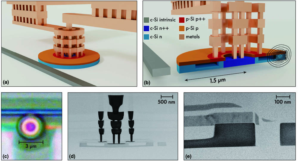
    Fig. 1. Perspective view of the MOSCAP modulator and microscope images of the fabricated device. (a) Full three-dimensional rendering of the modulator structure as designed; (b) device cross section, showing internal structure of the resonator, doping profiles of c-Si body and p-Si gate device layers, placement of metal contacts, and optical mode profile; (c) optical micrograph of the fabricated device; (d) TEM of the full device cross section, showing the resonator structure, bus waveguide, and lower four metal layers; (e) TEM zoom-in on the guiding core of the resonator and ring-bus coupling region.
    Experimental data from passive optical and DC EO device characterization (device with 32 kΩ/□ gate sheet resistance). (a) Optical transmission response of the MRM in O-band showing two resonances spaced by 8.5 THz or 48 nm FSR; (b) modulator optical response for gate voltages between −3 and 0 V, showing resonance blueshift due to free carrier inversion; (c) optical response for gate voltages between 0 and 4 V, showing resonance blueshift due to carrier accumulation.
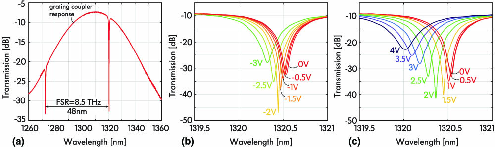
    Fig. 2. Experimental data from passive optical and DC EO device characterization (device with 32kΩ/ gate sheet resistance). (a) Optical transmission response of the MRM in O-band showing two resonances spaced by 8.5 THz or 48 nm FSR; (b) modulator optical response for gate voltages between 3 and 0 V, showing resonance blueshift due to free carrier inversion; (c) optical response for gate voltages between 0 and 4 V, showing resonance blueshift due to carrier accumulation.
    Experimental data from DC electrical and EO device characterization for different p-Si gate doping concentrations. (a) Dependence of gate sheet resistance on acceptor concentration; (b) resonance frequency shift versus gate voltage, showing up to 90 GHz shift for gate voltages between 0 and 4 V; (c) modulator shift efficiency at different bias points, showing 30 GHz/V resonance modulation efficiency above 2 V; (d) resonance intrinsic quality factor versus gate voltage.
    Fig. 3. Experimental data from DC electrical and EO device characterization for different p-Si gate doping concentrations. (a) Dependence of gate sheet resistance on acceptor concentration; (b) resonance frequency shift versus gate voltage, showing up to 90 GHz shift for gate voltages between 0 and 4 V; (c) modulator shift efficiency at different bias points, showing 30 GHz/V resonance modulation efficiency above 2 V; (d) resonance intrinsic quality factor versus gate voltage.
    Experimental results from high-speed EO characterization of modulators. (a) Normalized EO response of the modulator with gate sheet resistance of 32 kΩ/□; (b) dependence of EO 3 dB bandwidth on gate bias voltage for a few modulator variants with different gate doping concentrations; (c)–(e) optical eye diagrams at 5 Gbps acquired at several bias points of gate voltage and laser wavelength; (f) illustration of the MOSCAP cross section with half the capacitance of the original device; (g) eye diagram (10 Gbps) of the MRM with 2 times smaller capacitance; (h) illustration of the MOSCAP cross section with additional implants introduced for reducing series resistance while preserving resonance quality factor.
    Fig. 4. Experimental results from high-speed EO characterization of modulators. (a) Normalized EO response of the modulator with gate sheet resistance of 32kΩ/; (b) dependence of EO 3 dB bandwidth on gate bias voltage for a few modulator variants with different gate doping concentrations; (c)–(e) optical eye diagrams at 5 Gbps acquired at several bias points of gate voltage and laser wavelength; (f) illustration of the MOSCAP cross section with half the capacitance of the original device; (g) eye diagram (10 Gbps) of the MRM with 2 times smaller capacitance; (h) illustration of the MOSCAP cross section with additional implants introduced for reducing series resistance while preserving resonance quality factor.
    Hayk Gevorgyan, Anatol Khilo, Mark T. Wade, Vladimir M. Stojanović, Miloš A. Popović. Miniature, highly sensitive MOSCAP ring modulators in co-optimized electronic-photonic CMOS[J]. Photonics Research, 2022, 10(1): A1
    Download Citation