Abstract
This paper reports the material characteristics of In0.66Ga0.34As/InyAl1-yAs high electron mobility transistor (HEMT). The linearly graded InyAl1-yAs buffer layer was grown on InP substrates by gas source molecular beam epitaxy (GSMBE). The influence of InyAl1-yAs graded buffer layer with different thickness and different indium contents on the surface quality, the electron mobility and the concentrations of two-dimensional electron gas (2DEG) was studied. It was found that the electron mobility and concentration at 300 K (77 K) were 8570 cm2/(Vs)-1 (23200 cm2/(Vs)-1) and 3.255×1012 cm-2 (2.732×1012 cm-2). The surface morphology of the material was also well improved and the root mean square (RMS) was 0.154 nm when the InAlAs graded buffer layer thickness was 50 nm. And this study can provide strong support for the improvement of HEMT performance.Introduction
HEMT is an important solid-state device for millimeter-wave and terahertz-wave application. InP based InxGa1-xAs/InyAl1-yAs PHEMT has attracted more and more attention due to its excellent high frequency and low noise coefficient properties,which can be widely used in the field of electronic device[1-11]. The high barrier or deep well region leads to high electron saturation velocity and electron mobility of the PHEMT structure. How to improve electron mobility becomes an important problem to be solved.
Increasing the indium contents of the InGaAs channel is one of the ways to improve the electron mobility[12-15]. However,the problem of the lattice mismatch between the InGaAs channel with high indium contents and the InP substrate has not been solved perfectly in the InP-based HEMT structure[3]. If the indium contents of the InGaAs channel is continuously increased the lattice mismatch will become larger. Therefore,threading dislocation defects,3D islands and rough interface will occur at the material interface,which will lead to the decline in mobility[16-18]. There are many dislocation restriction mechanisms has been used to release the interface strain,such as graded buffer,dilute nitride buffer,super lattice compensated in strain layer,well-distributed thickness buffer,multiple layers of self-organized quantum dots,two-step growth technique,metamorphic lattice-mismatched growth[19-31]. InAlAs graded buffer layer can effectively reduce dislocation defects[32-33]. The high band gap of InAlAs can reduce the leakage current in HEMT devices[34-35]. The challenge to the growing of the InAlAs graded buffer layer is the linear graded in the indium contents,which leads to local composition accumulation and surface roughness[36-39].
In this paper,the influence of InyAl1-yAs graded buffer layer on the characteristics of InP-HEMT is systematically studied. Material properties of the InyAl1-yAs graded buffer layer are mainly investigated in different thickness and indium contents of InyAl1-yAs graded buffer layer.
1 Experiment
The fluxes of group Ⅲ elements indium(In),gallium(Ga),aluminum(Al)were controlled by adjusting effusion cell temperatures,respectively. The silicon(Si)was used as n-type doping source and the groupⅤelements P2 and As2 were obtained by cracking phosphine and arsine at 1000℃.
InP substrate was pre-degassed at about 350 °C in the preparation chamber for 1 hour. Using P2 flux to protect substrate surface when the substrate temperature approaches to 300℃. The substrate temperature is approximately 425℃ for 3 minutes until the(4×2)-(100)In-stable reconstruction occurs. It uses situ reflected high energy electron diffraction(RHEED)to monitor substrate surface reconstruction[40]. The structure quality,electron mobility,surface morphology,cross-sectional of all samples were characterized by Philips High Resolution X-ray Diffraction(HRXRD),Hall HL-5500,Bruker Atomic Force Microscopy(AFM),JEM-2100F Transmission Electron Microscope(TEM),respectively.
| Layer | Material | Thickness /nm |
|---|
| S.I InP Substrate |
| Contact layer | In0.65Ga0.35As | 25 |
| Contact layer | In0.52Al0.48As | 15 |
| Etch stop layer | InP | 4 |
| Barrier layer | In0.52Al0.48As | 8 |
| Doped layer | Si concentration | (2-4)×1012 cm-2 |
| Spacer layer | In0.52Al0.48As | 3 |
| Channel layer | In0.66Ga0.34As | 10 |
| Graded buffer layer | InyAl1-yAs | z(0,10,30,50,70,90) |
| Buffer layer | In0.52Al0.48As | 500-z |
Table 1. InP-HEMT structure
InP-HEMT structure illustrated in table 1 consists of a z nm InyAl1-yAs graded buffer layer,a 500-z nm In0.52Al0.48As buffer layer,a 10 nm In0.66Ga0.34As channel layer,a 3 nm In0.52Al0.48As spacer layer,a Si-doping concentration of 2-4×1012 cm-2,a 8 nm In0.52Al0.48As barrier layer,a 4 nm InP etch stop layer,a 15 nm In0.52Al0.48As contact layer,a 25 nm In0.65Ga0.35As contact layer.
2 Results and discussion
2.1 InAlAs graded buffer with different thickness
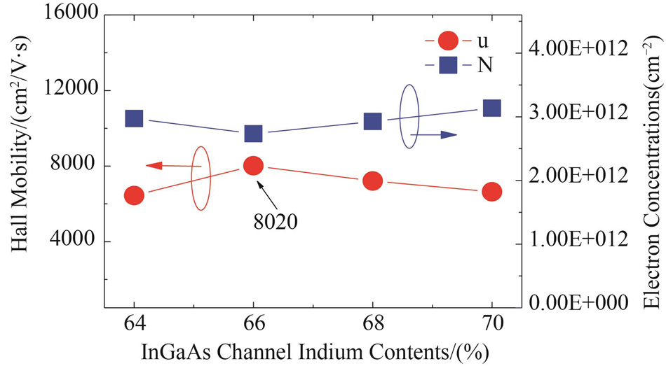
The mobility and electron concentration was studied in different indium contents of InGaAs channel. The results of four different indium contents channel are shown in Fig. 1. The highest electron mobility of 8020 cm2(vs)-1 was achieved. Increasing the indium contents of InGaAs channel can deepen the potential well,which confine more electrons and improve the mobility. As is shown in Table 2,different InAlAs graded buffer with thickness of 0 nm,10 nm,30 nm,50 nm,70 nm and 90 nm were designed. The aluminum contents of InyAl1-yAs was graded from 48% to 38%.

Figure 1.Hall mobility and electron concentrations in different channel indium contents
| Thincness/nm | 0 | 10 | 30 | 50 | 70 | 90 |
|---|
| FWHM/s | - | 131.2 | 207 | 39.7 | 188.9 | 168.3 |
| µ/cm2(vs)-1 | 8 020 | 8 030 | 8 260 | 8 570 | 8 230 | 7 710 |
| Ns/1012 cm-2 | 2.735 | 3.242 | 3.255 | 2.7 | 2.756 | 3.199 |
| InAlAs RMS/nm | 0.117 | 0.241 | 0.376 | 0.154 | 0.195 | 0.337 |
| InAlAs+InGaAs RMS/nm | 0.185 | 0.283 | 0.275 | 0.17 | 0.223 | 0.23 |
Table 2. Properties of InAlAs graded buffer layer with different thickness
According to the HRXRD image in Fig. 2,the single peak of sample a1 means that InAlAs and InP substrate is match lattice. Epitaxial peaks FWHM of sample a2,a3 and a5 are not a good result due to varying degrees of mismatch in the InAlAs material. Multiple epitaxial peaks appear in sample a6,which is caused by the InAlAs graded buffer layer interface strain. The FWHM of sample a4 is the best about 39.7 s,which indicates that the 50 nm InAlAs graded buffer layer can acquire better crystal quality.
Figure 2.HRXRD(004)ω-2θ scans for InAlAs graded buffer layer with different thickness
The InAlAs graded buffer layer with different thickness and the InGaAs channel layer were grown. AFM tapping mode on 5 µm×5 µm area was used to characterize the surface morphology of these samples. As is shown in Fig. 3,the RMS of sample t=0 nm is 0.117 nm and obviously better than that of other samples,which is due to the material lattice-matched. The best RMS is 0.154 nm when the thickness is 50 nm. In the 3D images of the sample t=50 nm can be seen the InAlAs surface is smooth and has no defects introduced. The surface quality of the sample lower than other thickness. The InAlAs surface has great fluctuation due to interfacial strain when t=90 nm. From the 3D image of t =90 nm,it can be observed that both sides of InAlAs graded buffer layer have obviously crimped,which indicates that the interface strain has occurred.
Figure 3.The surface morphology of the InAlAs graded buffer layer with different thickness
The channel material quality plays a critical role in the HEMT performance. Therefore,In0.66Ga0.34As channel materials grown on different thickness of InAlAs graded buffer layer were studied. Figure 4 demonstrate that the variation trend of samples RMS is roughly consistent with Fig. 3. It can be found that the sample t=50 nm RMS is 0.17 nm,which is obviously smaller than that of other samples. According to the 3D images of sample t=0 nm and t=50 nm,which shows the surface smooth and atomic layer particle size of sample t=50 nm is much better than sample t=0 nm. It can be explained that lattice mismatch between In0.66Ga0.34As channel and In0.52Al0.48As buffer layer causes surface defects in the HEMT. The InAlAs graded buffer layer can significantly release the stress caused by lattice mismatch.
Figure 4.The surface morphology of the InGaAs channel with different InAlAs graded buffer layer thickness
The mobility and electron concentration of InAlAs graded buffer layer with different thickness were characterized by HALL. Ultimately it can be found from the Fig. 5,when the InAlAs graded buffer layer thickness is 50 nm the electron mobility of 8 570 cm2(vs)-1 is higher. It verifies that the 50 nm InAlAs graded buffer can release the interface stress and provide a smooth interface to improve electron mobility. This is a good method to provide material performance based on the result of the experiment.
Figure 5.Hall mobility and electron concentrations in different InAlAs graded buffer layer thickness
2.2 InAlAs graded buffer with different indium contents
In order to more comprehensively characterize the effect of InAlAs graded buffer layer on material performance. The influence of different indium contents on material performance was investigated when InAlAs graded buffer layer thickness was 50 nm. The indium and aluminum contents of InyAl1-yAs were adjusted through the linear decreasing of aluminum source cell temperature. The results were shown in Table 3.
Graded InAlAs aluminum contents/(%) | 48 | 48→43 | 48→38 | 48→34 |
|---|
Graded InAlAs indium contents/(%) | 52 | 52→57 | 52→62 | 52→66 |
| µ/cm2(vs)-1 | 8020 | 8070 | 8570 | 7800 |
| Ns/1012cm-2 | 2.735 | 3.485 | 2.7 | 2.987 |
InAlAs RMS/nm | 0.117 | 0.197 | 0.154 | 0.287 |
| InAlAs+InGaAs RMS/nm | 0.185 | 0.293 | 0.17 | 0.217 |
Table 3. Properties of InAlAs graded buffer layer with different aluminum contents
The surface quality of 50 nm InAlAs graded buffer layer with different aluminum contents and In0.66Ga0.34As channel layer above InAlAs graded buffer layer were studied. The AFM images shown in Fig. 6 and Fig. 7,It can be seen the changing trend of four groups samples surface roughness approximately consistent. In Fig. 6,it illustrates that the RMS of In0.52Al0.48As is 0.117 nm. The 3D images show that atomic particles distribution uniformly,which indicated strain has not occurred on the material layer. The surface morphology is slightly worse after graded buffer layer was inserted. The RMS of 0.154 nm of sample Al 48%→38% was acquired. In the 3D image of sample Al 48%→34%,it shows the surface is undulation and the edge of the material rise and fall. The material layer is subjected to compressive stress with the linear of Al contents reduce to 34%. It indicates that the interface strain has occurred.
Figure 6.The surface morphology of the InAlAs graded buffer layer with different aluminum contents
Figure 7.The surface morphology of the InGaAs channel with different aluminum contents
In sample Al contents 48%→34% of Fig. 7. The RMS of 0.217 nm is not the best among the four samples. It can be seen from the 3D image,the InGaAs material layer tends to enlarge the lattice to compensate for the defects caused by the interface strain on the InAlAs graded buffer layer,and eventually forms a relatively rough InGaAs interface. In 3D image in sample Al contents 48%→43%,it shows that obvious strain has occurred at the edge of InGaAs material layer. The RMS of sample Al contents 48%→38% is significantly smaller than that of other samples. The reason is that the graded buffer layer In0.62Al0.38As and the channel layer In0.66Ga0.34As are approximately matched. The film quality can be improved by releasing interface strain. According to the corresponding 3D image,it can be clearly seen that the InGaAs interface smooth reach to atomic level.
Figure 8 and Fig. 9 shows that the TEM energy band spectrum and cross-sectional of InP-HEMT with 50 nm InAlAs graded buffer layer. The 50 nm InAlAs graded buffer layer is obtained by linearly reducing the aluminum contents. According to the cross-sectional of the material,It can be seen from Fig. 9,material layers thickness corresponds to the design thickness. The interface of InAlAs graded buffer layer and InGaAs channel layer is smooth and has no related strain defects.
Figure 8.TEM energy spectrum image of InP-HEMT with InAlAs graded buffer layer
Figure 9.TEM Cross-sectional image of InP-HEMT with InAlAs graded buffer layer
According to the Fig. 10,four groups different aluminum contents were compared. It can be found that the mobility was improved with the aluminum contents decreases from 48% to 38%. Because there is no strain between the InAlAs graded buffer layer and the InGaAs channel layer. In addition,the higher smooth and quality of the InGaAs channel layer interface promote the migration of 2DEG. The mobility and concentration of 300 K(77 K)were 8570 cm2/(Vs)-1(23200 cm2/(Vs)-1)and 3.255×1012 cm-2(2.732×1012 cm-2).
Figure 10.Hall mobility and electron concentrations in different InAlAs graded buffer layer aluminum contents
3 Conclusion
In this paper,the influence of different thickness and different indium contents of InyAl1-yAs graded buffer layer on the surface quality,the mobility and the concentrations of two-dimensional electron gas(2DEG)was demonstrated. It is found that the mobility and concentration at 300 K(77 K)were 8570 cm2/(Vs)-1(23200 cm2/(Vs)-1)and 3.255×1012 cm-2(2.732×1012 cm-2). The surface morphology of the material was also well improved and the RMS was 0.154 nm when the InAlAs graded buffer layer thickness was 50 nm. These results support that InAlAs graded buffer layer can reduce the residual strain value,decrease the dislocation defects,enhance the interface quality,and improve the hall mobility,significantly.
References
[1] W R Deal, K Leong, V Radisic et al. Low noise amplification at 0.67 THz using 30 nm InP HEMTs. IEEE Microwave & Wireless Components Letters, 21, 368-370(2011).
[2] R A Metzger, A S Brown, L G Mccray et al. Structural and electrical properties of low temperature GaInAs. Journal of vacuum science & technology B, 11, 798-801(1993).
[3] K Matsuno. High-quality InxGa1-xAs/InAlAs modulation-doped heterostructures grown lattice-mismatched on GaAs substrates. Journal of Crystal Growth, 111, 313-317(1991).
[4] K M K H Leong, X Mei, W Yoshida et al. A 0.85 THz low noise amplifier using InP HEMT transistors. IEEE Microwave & Wireless Components Letters, 25, 397-399(2015).
[5] X Mei, W Yoshida, M Lange et al. First demonstration of amplification at 1 THz using 25-nm InP high electron mobility transistor process. IEEE Electron Device Letters, 36, 327-329(2015).
[6] W R Deal, K Leong, A Zamora et al. Recent progress in scaling InP HEMT TMIC technology to 850 GHz, 1-3(2014).
[7] V Radisic, K Leong, X Mei et al. Power amplification at 0.65 THz using InP HEMTs. IEEE Transactions on Microwave Theory & Techniques, 60, 724-729(2012).
[8] E P A M Bakkers, J A Van Dam, S De Franceschi et al. Epitaxial growth of InP nanowires on germanium. Nature materials, 3, 769-773(2004).
[9] K Shinohara. 547-GHz f_t In_Ga_As-In_Al_As HEMTs With Reduced Source and Drain Resistance. IEEE Electron Device Lett, 25, 241-243(2004).
[10] N Pan, J Elliott, H Hendriks et al. InAlAs/InGaAs high electron mobility transistors on low temperature InAlAs buffer layers by metalorganic chemical vapor deposition. Applied Physics Letters, 66, 212-214(1995).
[11] U J Lewark, T Zwick, A Tessmann et al. Active 600GHz frequency multiplier-by-Six S-MMICs for submillimeter-wave generation, 1-3(2014).
[12] T Nakayama, H Miyamoto. Modulation doped structure with thick strained InAs channel beyond the critical thickness. Journal of Crystal Growth, 201, 782-785(1999).
[13] P C Chao, A J Tessmer, K Duh et al. W-band low-noise InAlAs/InGaAs lattice-matched HEMTs. IEEE Electron Device Letters, 11, 59-62(1990).
[14] T Nakayama, H Miyamoto, E Oishi et al. High electron mobility 18300 cm2/V·s in the InAIAs/lnGaAs pseudomorphic structure obtained by channel indium composition modulation. Journal of Electronic Materials, 25, 555-558(1996).
[15] R Lai, P K Bhattacharya, D Yang et al. Characteristics of 0.8- and 0.2-μm gate length InxGa 1-xAs/In0.52Al0.48As/InP (0.53⩽x⩽0.70) modulation-doped field-effect transistors at cryogenic temperatures. IEEE Transactions on Electron Devices, 39, 2206-2213(1992).
[16] Y Fedoryshyn, M Ping, J Faist et al. Electron. Lab., ETH Zurich, Zürich, Switzerland. Quantum Electronics IEEE Journal of, 48, 885-890(2012).
[17] E Y Lee, S Bhargava, M A Chin et al. Observation of misfit dislocations at the InxGa1-xAs/GaAs interface by ballistic-electron-emission microscopy. Applied Physics Letters, 69, 940-942(1996).
[18] S-X Zhou, M Qi, L-K Ai et al. Growth condition optimization and mobility enhancement through inserting AlAs monolayer in the InP-based InxGa1- xAs/In0. 52Al0. 48As HEMT structures. Chinese Physics B, 25, 096801(2016).
[19] M A Tischler, T Katsuyama, N A El-Masry et al. Defect reduction in GaAs epitaxial layers using a GaAsP‐InGaAs strained‐layer superlattice. Applied Physics Letters, 46, 294-296(1985).
[20] B Lee, J H Baek, J H Lee et al. Optical properties of InGaAs linear graded buffer layers on GaAs grown by metalorganic chemical vapor deposition. Applied physics letters, 68, 2973-2975(1996).
[21] Y Gu, Y G Zhang, K Wang et al. InP-based InAs/InGaAs quantum wells with type-I emission beyond 3 μm. Applied Physics Letters, 99, 445(2011).
[22] M K Hudait, Y Lin, S A Ringel. Strain relaxation properties of InAsyP1-y metamorphic materials grown on InP substrates. Journal of Applied Physics, 105, 061643-061643-061612(2009).
[23] J Kirch, T Garrod, S Kim et al. InAs_yP_(1-y) metamorphic buffer layers on InP substrates for mid-IR diode lasers. Journal of Crystal Growth, 312, 1165-1169(2010).
[24] I S Vasil’evskii, G B Galiev, E A Klimov et al. Interrelation of the construction of the metamorphic InAlAs/InGaAs nanoheterostructures with the InAs content in the active layer of 76-100% with their surface morphology and electrical properties. Semiconductors, 45, 1158(2011).
[25] J Tersoff. Dislocations and strain relief in compositionally graded layers. Applied physics letters, 62, 693-695(1993).
[26] I J Fritz, S T Picraux, L R Dawson et al. Dependence of critical layer thickness on strain for InxGa1-xAs/GaAs strained‐layer superlattices. Applied Physics Letters, 46, 967-969(1985).
[27] Y Y Cao, Y G Zhang, Y Gu et al. 2.7 m InAs quantum well lasers on InP-based InAlAs metamorphic buffer layers. Applied Physics Letters, 102, 458(2013).
[28] Y Gu, Y Zhang, K Wang et al. InAlAs Graded Metamorphic Buffer with Digital Alloy Intermediate Layers. Japanese Journal of Applied Physics, 51, 0205(2012).
[29] X Liu, H Song, G Q Miao et al. Influence of thermal annealing duration of buffer layer on the crystalline quality of In 0.82 Ga 0.18 As grown on InP substrate by LP-MOCVD. Applied Surface Science, 257, 1996-1999(2011).
[30] A Sayari, N Yahyaoui, A Meftah et al. Residual strain and alloying effects on the vibrational properties of step-graded InxAl1- xAs layers grown on GaAs. Journal of luminescence, 129, 105-109(2009).
[31] F Capotondi, G Biasiol, I Vobornik et al. Two-dimensional electron gas formation in undoped In0.75Ga0.25As/In0.75Al0.25As quantum wells. Journal of vacuum ence & technology B, 22, 702-706(2004).
[32] J.-I Chyi,, Shieh et al. Material properties of compositional graded InxGa1-xAs and InxAl1-xAs epilayers grown on GaAs substrates. Journal of Applied Physics, 79, 8367-8367(1996).
[33] Y Cordier, D Ferre. InAlAs buffer layers grown lattice mismatched on GaAs with inverse steps. Journal of crystal growth, 201, 263-266(1999).
[34] W E H Hoke, C S Whelan. Metamorphic HEMT technology exemplified by InAlAs/InGaAs/GaAs HEMTs. Lattice Eng, 229(2012).
[35] D Kohen, X S Nguyen, R I Made et al. Preventing phase separation in MOCVD-grown InAlAs compositionally graded buffer on silicon substrate using InGaAs interlayers - ScienceDirect. Journal of Crystal Growth, 478, 64-70(2017).
[36] N J Quitoriano, E A Fitzgerald. Relaxed, high-quality InP on GaAs by using InGaAs and InGaP graded buffers to avoid phase separation. Journal of Applied Physics, 102, 152101-152110(2007).
[37] Y Sun, J Dong, S Yu et al. High quality InP epilayers grown on GaAs substrates using metamorphic AlGaInAs buffers by metalorganic chemical vapor deposition. Journal of Materials Science: Materials in Electronics, 28, 745-749(2017).
[38] F Glas. Elastic state and thermodynamical properties of inhomogeneous epitaxial layers: Application to immiscible III‐V alloys. Journal of Applied Physics, 62, 3201-3208(1987).
[39] J Tersoff. Stress-driven alloy decomposition during step-flow growth. Physical Review Letters, 77, 2017(1996).
[40] F Tian, L Ai, A Xu et al. InGaAsPBi grown on InP substrate by gas source molecular beam epitaxy. Materials Research Express, 8, 026404(2021).