• Chinese Optics Letters
  • Vol. 20, Issue 7, 071301 (2022)
Sumei Wang1, Jinhua Zhao1、*, Jinjun Gu1, Mingyang Bu1, Li Fan1, Shuang Li1, Xifeng Qin1, Yicun Yao2, Yingying Ren3, and Lei Wang4
Author Affiliations
  • 1School of Science, Shandong Jianzhu University, Jinan 250101, China
  • 2Shandong Key Laboratory of Optical Communication Science and Technology, School of Physical Science and Information Technology, Liaocheng University, Liaocheng 252059, China
  • 3Shandong Provincial Engineering and Technical Center of Light Manipulations & Shandong Provincial Key Laboratory of Optics and Photonic Device, School of Physics and Electronics, Shandong Normal University, Jinan 250014, China
  • 4School of Physics, Shandong University, Jinan 250100, China
  • show less
    DOI: 10.3788/COL202220.071301 Cite this Article Set citation alerts
    Sumei Wang, Jinhua Zhao, Jinjun Gu, Mingyang Bu, Li Fan, Shuang Li, Xifeng Qin, Yicun Yao, Yingying Ren, Lei Wang. LiNbO3 channel and ridge waveguides based on helium ion implantation combined with lithography and precise diamond dicing[J]. Chinese Optics Letters, 2022, 20(7): 071301 Copy Citation Text show less
    Fabrication methods of LN waveguides: (a) channel guide; (b) ridge guide.
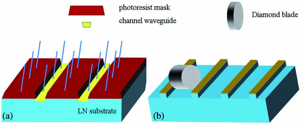
    Fig. 1. Fabrication methods of LN waveguides: (a) channel guide; (b) ridge guide.
    (a) Dpa profile of 500 keV He ions with the fluence of 1.5 × 10¹⁶ ions/cm2 implanted into LN crystal by SRIM 2013; (b) reconstructed RIP of the LN waveguide after annealing at 260°C for 30 min at 633 nm.
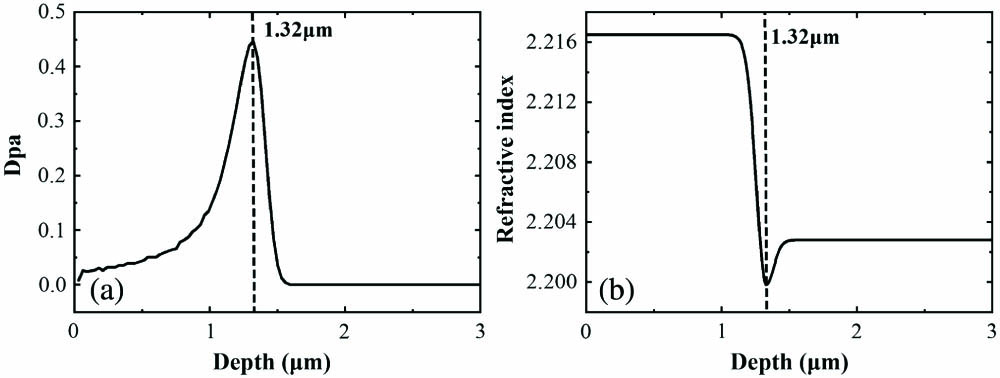
    Fig. 2. (a) Dpa profile of 500 keV He ions with the fluence of 1.5 × 10¹⁶ ions/cm2 implanted into LN crystal by SRIM 2013; (b) reconstructed RIP of the LN waveguide after annealing at 260°C for 30 min at 633 nm.
    (a) Profile of the TM0 guided mode simulated by BPM [one-dimensional (1D)]; (b) the modal intensity profile of TM0 mode computed by the BPM (2D); (c) near-field image of the TM0 mode by use of the end-face coupling method.
    Fig. 3. (a) Profile of the TM0 guided mode simulated by BPM [one-dimensional (1D)]; (b) the modal intensity profile of TM0 mode computed by the BPM (2D); (c) near-field image of the TM0 mode by use of the end-face coupling method.
    Optical microscope image (×500) of the end face of waveguides after polishing: (a) WG10; (b) WG15; (c) WG25.
    Fig. 4. Optical microscope image (×500) of the end face of waveguides after polishing: (a) WG10; (b) WG15; (c) WG25.
    Reconstructed RIP of the waveguide: (a) WG10; (b) WG15.
    Fig. 5. Reconstructed RIP of the waveguide: (a) WG10; (b) WG15.
    (a)–(c) Near-field image of WG10 quasi-TM modes from the end face of the sample captured by a CCD camera; (d)–(f) modal intensity profile computed by finite difference (FD)-BPM: quasi-TM00, TM10, TM20 modes. The color scale, which represents the relative light intensity, is shown also.
    Fig. 6. (a)–(c) Near-field image of WG10 quasi-TM modes from the end face of the sample captured by a CCD camera; (d)–(f) modal intensity profile computed by finite difference (FD)-BPM: quasi-TM00, TM10, TM20 modes. The color scale, which represents the relative light intensity, is shown also.
    (a)–(c) Near-field image of WG15 quasi-TM modes from the end face of the sample captured by a CCD camera; (d)–(f) modal intensity profile computed by FD-BPM. The color scale, which represents the relative light intensity, is shown also.
    Fig. 7. (a)–(c) Near-field image of WG15 quasi-TM modes from the end face of the sample captured by a CCD camera; (d)–(f) modal intensity profile computed by FD-BPM. The color scale, which represents the relative light intensity, is shown also.
    Experimental setup used with the end-face coupling method. Obj, microscope objective lens; location 1, the first position where the light power was measured; location 2, the second position where the light power was measured.
    Fig. 8. Experimental setup used with the end-face coupling method. Obj, microscope objective lens; location 1, the first position where the light power was measured; location 2, the second position where the light power was measured.
    WaveguideCoupling EfficiencyPropagation Loss (dB/cm)
    WG1050.16%3.42
    WG2546.55%1.97
    WG1546.72%12.4
    Table 1. Coupling Efficiencies and Propagation Losses of the 2D Waveguides at 633 nm for TM Polarization
    Sumei Wang, Jinhua Zhao, Jinjun Gu, Mingyang Bu, Li Fan, Shuang Li, Xifeng Qin, Yicun Yao, Yingying Ren, Lei Wang. LiNbO3 channel and ridge waveguides based on helium ion implantation combined with lithography and precise diamond dicing[J]. Chinese Optics Letters, 2022, 20(7): 071301
    Download Citation