• Photonics Research
  • Vol. 6, Issue 3, 168 (2018)
Amir Ghobadi1、2, Hodjat Hajian1, Alireza Rahimi Rashed1, Bayram Butun1, and Ekmel Ozbay1、2、3、4、*
Author Affiliations
  • 1NANOTAM-Nanotechnology Research Center, Bilkent University, 06800 Ankara, Turkey
  • 2Department of Electrical and Electronics Engineering, Bilkent University, 06800 Ankara, Turkey
  • 3Department of Physics, Bilkent University, 06800 Ankara, Turkey
  • 4UNAM-Institute of Materials Science and Nanotechnology, Bilkent University, 06800 Ankara, Turkey
  • show less
    DOI: 10.1364/PRJ.6.000168 Cite this Article Set citation alerts
    Amir Ghobadi, Hodjat Hajian, Alireza Rahimi Rashed, Bayram Butun, Ekmel Ozbay. Tuning the metal filling fraction in metal-insulator-metal ultra-broadband perfect absorbers to maximize the absorption bandwidth[J]. Photonics Research, 2018, 6(3): 168 Copy Citation Text show less
    (a) Schematic representation of the MIM design. (b) Cross-sectional SEM image of the fabricated structure and (c) its optical image for two different DI values of 50 nm and 60 nm, where the metal thickness is chosen to be 5 nm. (d) Relative permittivity values of Al2O3 (for bare and 800°C annealed cases) and Cr layers.
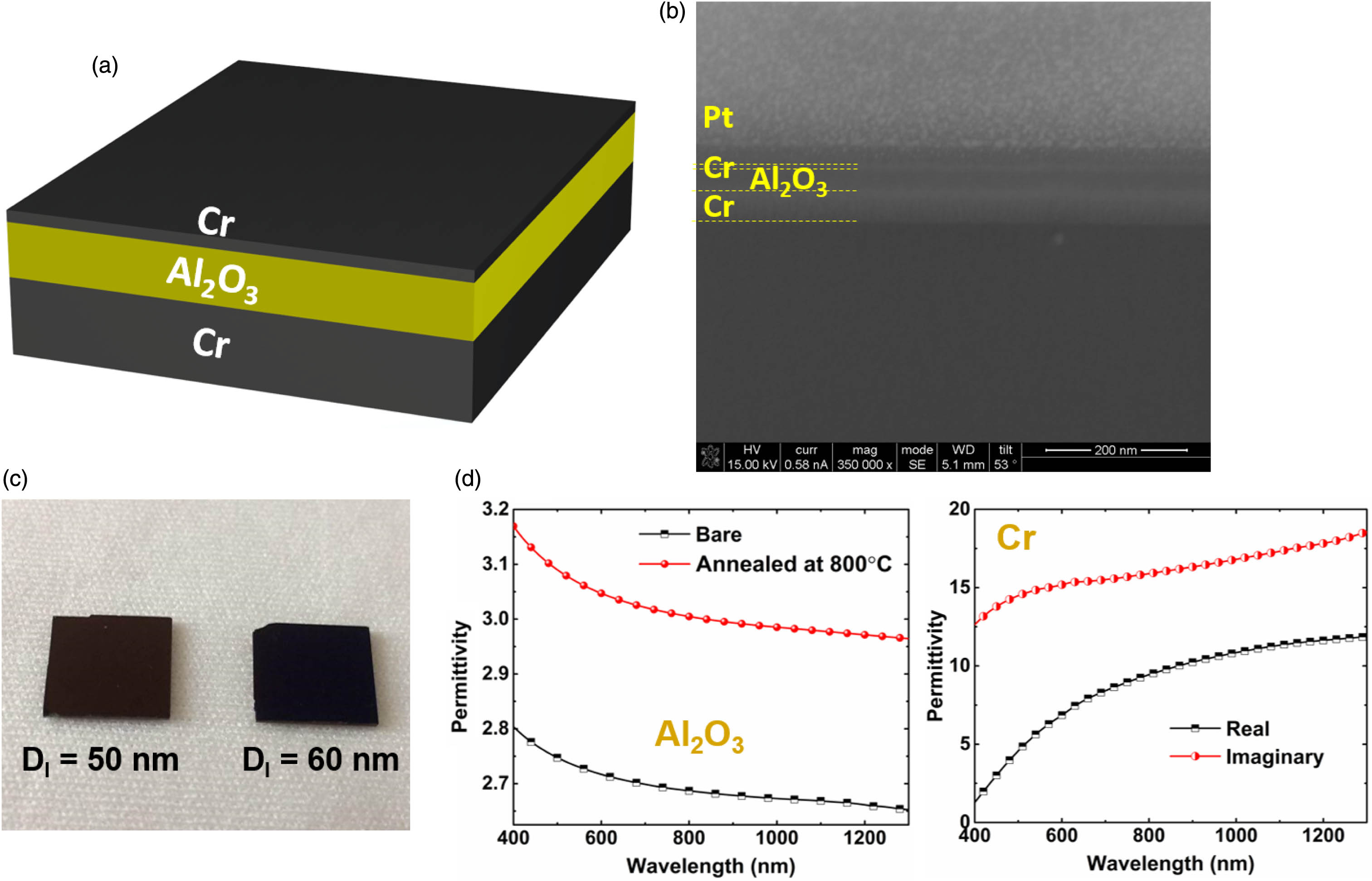
    Fig. 1. (a) Schematic representation of the MIM design. (b) Cross-sectional SEM image of the fabricated structure and (c) its optical image for two different DI values of 50 nm and 60 nm, where the metal thickness is chosen to be 5 nm. (d) Relative permittivity values of Al2O3 (for bare and 800°C annealed cases) and Cr layers.
    Simulated absorption spectra of the MIM design for (a) different DI values (where the metal thickness is fixed at 5 nm) and (b) different DM values (where the insulator thickness is fixed at 60 nm). (c) Absorbed power contour plot in different layers of MIM design as a function of incident light wavelength. (d) Measured absorption spectra of fabricated samples with two different DI values of 50 nm and 60 nm. The angular absorption responses of the fabricated devices with two different DI values of (e) 50 nm and (f) 60 nm.
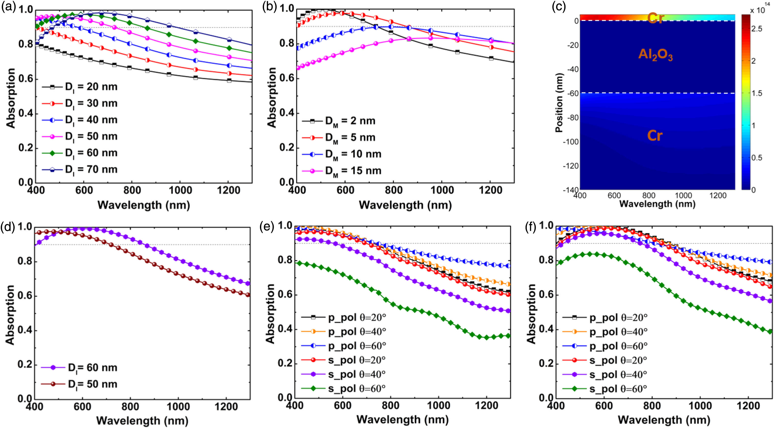
    Fig. 2. Simulated absorption spectra of the MIM design for (a) different DI values (where the metal thickness is fixed at 5 nm) and (b) different DM values (where the insulator thickness is fixed at 60 nm). (c) Absorbed power contour plot in different layers of MIM design as a function of incident light wavelength. (d) Measured absorption spectra of fabricated samples with two different DI values of 50 nm and 60 nm. The angular absorption responses of the fabricated devices with two different DI values of (e) 50 nm and (f) 60 nm.
    (a) Schematic representation of the MIM design used for the TMM model and (b) the corresponding contour plot showing the reflection value at the wavelength of 800 nm for a 15 nm thick top ideal material as a function of real and imaginary parts. The calculated real and imaginary parts of permittivity values and their matching with the tolerable ideal region for two different metal thicknesses of (c) DM1=5 nm, and (d) DM1=15 nm.
    Fig. 3. (a) Schematic representation of the MIM design used for the TMM model and (b) the corresponding contour plot showing the reflection value at the wavelength of 800 nm for a 15 nm thick top ideal material as a function of real and imaginary parts. The calculated real and imaginary parts of permittivity values and their matching with the tolerable ideal region for two different metal thicknesses of (c) DM1=5  nm, and (d) DM1=15  nm.
    Absorption spectra of the MIM design for different DI and DM values for three different filling fractions of (a), (b) 0.8, (c), (d) 0.6, and (e), (f) 0.4.
    Fig. 4. Absorption spectra of the MIM design for different DI and DM values for three different filling fractions of (a), (b) 0.8, (c), (d) 0.6, and (e), (f) 0.4.
    (a) Measured absorption spectra of dewetted samples at different annealing temperatures. Inset shows the magnified image of the results to clearly depict the absorption of upper and lower edges for three different dewetted samples. (b) Corresponding SEM images showing their surface morphology (the scale bars are all 2 μm). The angular absorption responses for p- and s-polarized incident light beams for dewetted samples at different temperatures of (c) 800°C, (d) 850°C, and (e) 900°C.
    Fig. 5. (a) Measured absorption spectra of dewetted samples at different annealing temperatures. Inset shows the magnified image of the results to clearly depict the absorption of upper and lower edges for three different dewetted samples. (b) Corresponding SEM images showing their surface morphology (the scale bars are all 2 μm). The angular absorption responses for p- and s-polarized incident light beams for dewetted samples at different temperatures of (c) 800°C, (d) 850°C, and (e) 900°C.
    Amir Ghobadi, Hodjat Hajian, Alireza Rahimi Rashed, Bayram Butun, Ekmel Ozbay. Tuning the metal filling fraction in metal-insulator-metal ultra-broadband perfect absorbers to maximize the absorption bandwidth[J]. Photonics Research, 2018, 6(3): 168
    Download Citation