Abstract
In this paper, we propose a methodology to maximize the absorption bandwidth of a metal-insulator-metal (MIM) based absorber. The proposed structure is made of a multilayer design. At the initial step, the optimum MIM planar design is fabricated and optically characterized. The results show absorption above 0.9 from 400 nm to 850 nm. Afterward, the transfer matrix method is used to find the optimal condition for the perfect light absorption in an ultra-broadband frequency range. This modeling approach predicts that changing the filling fraction of the top Cr layer can extend light absorption toward longer wavelengths. We experimentally proved that the use of proper top Cr thickness and annealing temperature leads to a nearly perfect light absorption from 400 nm to 1150 nm, which is much broader than that of a planar design. Therefore, while keeping the overall process lithography-free, the absorption functionality of the design can be significantly improved. The results presented here can serve as a beacon for future performance-enhanced multilayer designs where a simple fabrication step can boost the overall device response without changing its overall thickness and fabrication simplicity.1. INTRODUCTION
In the last few decades, the use of metamaterials to manipulate light–matter interaction has attracted a great deal of attention, owing to their extraordinary optical response that cannot be found in natural materials. The realization of perfect light absorption by the confinement of the light in subwavelength dimensions is one of these attributes [1,2]. An ideal absorber should have unity strength, which means harvesting the whole incident light. Depending on the device configuration and the materials, this perfect absorption can be attained in a narrow or a broad frequency range. While these narrowband absorbers are of great interest for sensing and spectroscopy applications [3–9], several other areas such as photovoltaic and thermal photovoltaic [10–15], steam generation [16,17], and photodetection [18] require the spectral broadness.
Up to now, different three-dimensional (3D) designs have been employed to obtain ultra-broadband perfect absorbers. The 3D nanostructures, such as densely packed nanowires [19], nanotubes [15], tapered grooves [20–22], and pyramidal designs [23,24], are examples of these architectures. However, these designs are bulky and incompatible for monolithic integration. Therefore, planar structures that can provide similar functionality in much smaller dimensions and volumes became a topic of intensive investigations in recent years. In the first studies, scientists proved the absorption capability of single-layer plasmonic metal nanostructures [1,8,25–27]. However, due to the lack of a trapping scheme, the absorption was not efficient in these configurations. Later, a metal-insulator-metal (MIM) configuration was employed to improve the absorption strength of the structure [3,28–38]. However, in all of the above cases, the operational bandwidth (BW) of near-unity absorption was not broad. In one of the pioneer studies in this field, Aydin et al. reported an average absorption above 0.71 in the range of 400 nm to 700 nm by utilizing a symmetrical arrangement of a crossed trapezoid array in an MIM cavity configuration where the spacer layer thickness was much smaller than the incident light wavelength [39]. Later, several different plasmonic units were utilized to improve the absorption BW and strength of the design [12,40–47]. However, the main drawback of all the aforementioned MIM designs was their fabrication complexity. Fabrication of the top nanostructured layer is carried out using electron beam lithography (EBL), which is not only a complex fabrication route but is also not suitable for upscaling of the designs. Therefore, the realization of ultra-broadband perfect absorbers with EBL-free designs has been the subject of many studies in recent years. For this aim, adopting a modeling approach, to obtain the ideal case for perfect light absorption, is of great importance. It should be mentioned that previous studies have utilized a perfectly impedance-matched sheet (PIMS) approach to provide efficient light-material interaction in an ultra-broadband frequency range [48–51]
Recently, it was theoretically proven that the periodic arrangement of planar metal-insulator (MI) pairs with proper thicknesses can provide near-perfect light absorption in a broad wavelength range [52]. In this multilayered design, the absorption BW gets wider as we increase the number of pairs. Therefore, due to their planar nature, which makes it a lithography-free design, these structures are envisioned to be excellent options for large-scale production. Up to now, several different metal and insulator pairs were utilized to obtain ultra-broadband light absorption in an MI-pair-based architecture [53–59]. However, the absorption in this design is concentrated in the middle thin metal layers, which are sealed by two insulator layers. Therefore, the absorbed power cannot interact with the external stimulation, which is a crucial requirement in some of the applications. Therefore, proposing a design configuration that can satisfy all of the above-mentioned requirements would be the ultimate goal in the design of an ultra-broadband perfect absorber. A recent study showed that the use of thin lossy metals such as chromium (Cr) can satisfy all the aforementioned requirements. In the paper, the authors showed that MIM stack of , in which the top Cr layer is 3 nm thick, can offer a nearly perfect light absorption from 450 nm to 850 nm [60]. The proposed EBL-free design also has an omnidirectional response that retains its high absorption amplitude even at wide incidence angles.
In this paper, an EBL-free, large-scale compatible MIM absorber design is utilized to acquire nearly perfect light absorption in an ultra-broadband wavelength regime. In the proposed design, Cr and are employed as metal and insulator layers. In the first step, the optimum configuration is achieved using numerical simulations, and the design is fabricated and characterized. According to the characterization results, absorption above 0.9 was obtained in a wavelength range of 400 nm to 850 nm, which is in line with the previous study [60]. Later, a systematic modeling approach based on the transfer matrix method (TMM) is conducted on the MIM configuration to find the ideal top metal characteristics. According to the estimations of this modeling, by tuning the filling fraction (FF) of the metal structure, the absorption edge can be significantly shifted toward larger wavelengths. To tune the FF of the metal, a large-scale compatible dewetting process is applied to the fabricated MIM stacks. The choice of proper top metal thickness and annealing temperature leads to an absorption above 0.9 throughout an ultra-broadband wavelength range, spanning from 400 nm to 1150 nm. Therefore, as a consequence of applying a simple annealing step, the absorption BW of 450 nm for a planar design is improved to an amount of 750 nm for the dewetted sample. Comparing with the previous study that uses planar bare layers in an MIM configuration [60], this design strategy can significantly improve the absorption bandwidth by tuning the metal FF. In other words, the proposed design proves that an optimum metal FF can greatly improve the absorption capability of the design. To the best of our knowledge, besides its ease of fabrication and large-scale compatibility, this design has the widest absorption spectra among all the reported MIM-based visible light absorbers. Moreover, the angular response of the design stays high even at angles as wide as 60°. The findings of this study reveal that a simple annealing step can substantiate the functionality of the MIM design without changing the design dimensionality and complexity. These results can be also extended to other types of MI-based optical designs.
2. RESULTS AND DISCUSSIONS
Figure 1(a) provides a schematic representation of the proposed design that is made of an MIM stack. In this configuration, the bottom layer (which is Cr in this case) is a thick metallic coating that acts as a reflecting mirror. On top of this mirror, a spacer and a thin absorbing metal layer are deposited. This MIM architecture makes a cavity that is able to trap and harvest light in a specific frequency range. In our case, the bottom Cr layer is chosen to be 100 nm thick. This layer is deposited using the thermal evaporation technique. Later, the prepared samples are transferred into the atomic layer deposition (ALD) chamber to coat the layer in our desired thickness of . Finally, the top thin Cr layer with a thickness of is coated on the samples using thermal evaporation. Figure 1(b) represents a cross-sectional view of scanning electron microscopy (SEM) images of the MIM structure that proves the successful formation of all three layers. To take the SEM image, the focused ion beam (FIB) is used to prepare a cross section of the sample by milling a trench perpendicular to the surface. In FIB milling, because the bombarded ions can etch the sample surface and consequently change the thickness of sample’s upper layer, we deposit a thin layer of Pt before starting the etching process. The fabricated MIM stacks with two different insulator thicknesses of , 60 nm are depicted in Fig. 1(c). Finally, the permittivity values of the deposited Cr and layers have been extracted using J. A. Woollam Co. Inc. V-VASE ellipsometer in a wavelength range of 400 nm to 1300 nm [see Fig. 1(d)]. It should be mentioned that the permittivity values have been extracted for bare and 800°C annealed samples. The obtained permittivity data shows that, upon conducting annealing process, permittivity values get slightly larger, which is in line with a previous study [61].
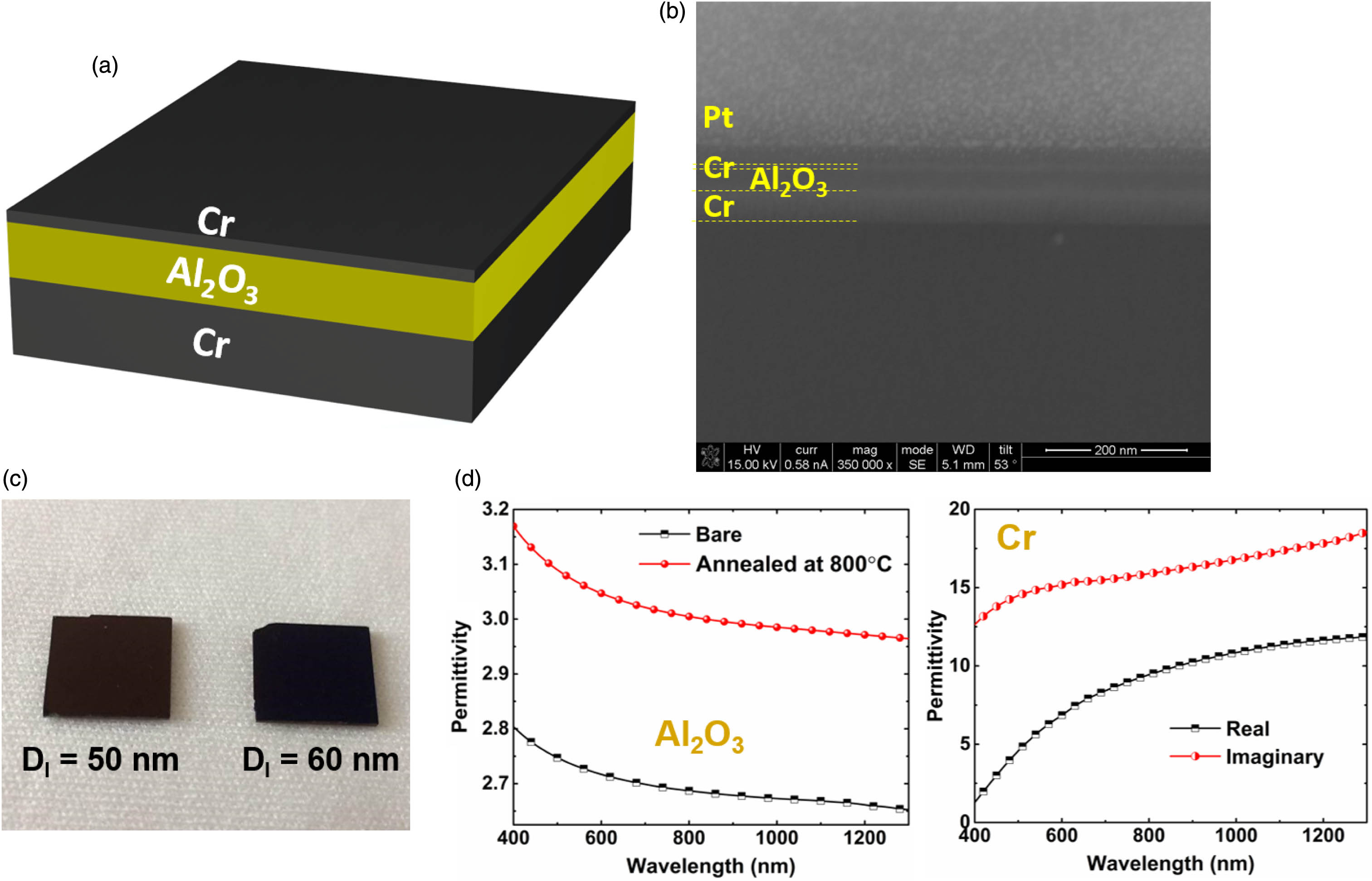
Figure 1.(a) Schematic representation of the MIM design. (b) Cross-sectional SEM image of the fabricated structure and (c) its optical image for two different values of 50 nm and 60 nm, where the metal thickness is chosen to be 5 nm. (d) Relative permittivity values of (for bare and 800°C annealed cases) and Cr layers.
For the first step, numerical simulations are conducted on the impact of different geometries on the absorption capacity of the MIM structure. For this aim, a commercial finite-difference time-domain (FDTD) software package (Lumerical FDTD Solutions) [62] is utilized. In all the simulations, a broadband plane wave (spanning from 400 nm to 1300 nm) with a specified polarization and incidence angle is illuminated on the sample. The absorption of the system can be calculated using the following formula of . Considering the fact that the bottom metal layer is a thick metal coating that reflects all the light back into the cavity, the transmission of the MIM design is equal to zero. Therefore, the above-mentioned formula is simplified to . Therefore, the absorption of the MIM design is calculated using the reflection monitoring data. For the permittivity values of Cr and , the experimental data have been imported to the material library. To begin with, the impact of insulator layer thickness () on the absorption spectra of the structure is explored. For this purpose, the top metal layer thickness is fixed at , and is swept from 20 nm to 70 nm. As Fig. 2(a) implies, increasing the insulator thickness introduces a spectral redshift on the absorption profile of the sample, rather than changing its intensity. To have a better qualitative comparison, the threshold for nearly perfect absorption is chosen as 0.9. To cover the whole visible spectrum, the lower absorption edge should locate at a wavelength around 400 nm, and the upper one should extend as long as possible. Therefore, the insulator layer thickness is fixed at 60 nm, and a new sweep is performed on the top metal thickness. Figure 2(b) depicts how the absorption strength is influenced by the metal layer thickness. Based on this panel, the absorption upper edge gets a redshift as we go from 2 nm to 5 nm. However, at thicknesses above 10 nm, a gradual loss is experienced on the light absorption strength in which the 15 nm thick case has an absorption entirely below 0.9. Taking all the above results into consideration, the optimum case of this planar design is and . The absorption profile of the structure, as a function of incident light wavelength, is also depicted in Fig. 2(c). As expected, the main portion of light gets absorbed in the top lossy thin Cr metal. In fact, this structure is acting as a low-quality-factor Fabry–Perot resonator. To evaluate our numerical findings, the proposed designs have been fabricated and experimentally characterized. For this aim, two samples with two different insulator layer thicknesses of and 60 nm have been fabricated. In both samples, the top metal thickness is . The fabrication route of the proposed design can be briefly explained as follows. First, the diced silicon substrates are cleaned using a standard cleaning process with piranha and hydrofluoric acid (HF) solutions. Afterward, a 100 nm thick Cr layer was deposited on top of these substrates using a thermal evaporator. The depositions were carried out at 250°C in an ALD reactor (Cambridge Nanotech Savannah S100) employing solution as the deposition precursor. The pulse and purge durations were 0.015 and 10 s, respectively. The growth rate was found to be 1.01 A° per cycle. Finally, the thin top Cr layer is deposited with the thermal evaporation system. To optically characterize the stack, the normal reflection measurements for the wavelength range of 600 nm to 1300 nm were carried out using Fourier transform infrared spectroscopy (Bruker); for the remaining part of the visible spectrum, we used a homemade reflection measurement setup in which a halogen illuminator is connected to a microscope and directed perpendicular to a sample, and the reflected light from the microscope was fed to a Newport OSM2 spectrometer. The data were collected by interfacing the spectrometer with a personal computer (PC). Moreover, the angle-resolved reflection characterizations were carried out using an J. A. Woollam Co. Inc. V-VASE ellipsometer for different angles of incidence and polarization. As can be clearly seen in Fig. 2(d), a nearly perfect agreement between simulations and characterization results can be obtained for both fabricated samples. The image of the MIM absorber is depicted in Fig. 1(c). Similar to the simulation results, absorption above 0.9 is attained from 400 nm up to 850 nm. In other words, the operation bandwidth of this system is found to be 450 nm. The angular absorption capacity of these two configurations is also compared in Figs. 2(e) and 2(f). Looking at the oblique angle responses of these two devices, we can clearly see that the absorption is kept high even at incidence angels as high as 60°. In the s-polarized excitation, the absorption spectra experience a gradual fall in their amplitude. However, in the case of p-polarized incident light, the absorption amplitude is improved at longer wavelengths, which is due to the increase in the optical path of light inside the cavity.

Figure 2.Simulated absorption spectra of the MIM design for (a) different values (where the metal thickness is fixed at 5 nm) and (b) different values (where the insulator thickness is fixed at 60 nm). (c) Absorbed power contour plot in different layers of MIM design as a function of incident light wavelength. (d) Measured absorption spectra of fabricated samples with two different values of 50 nm and 60 nm. The angular absorption responses of the fabricated devices with two different values of (e) 50 nm and (f) 60 nm.
Based on aforementioned findings, this MIM-based lithography-free structure does not have only a simple fabrication route but also provides a high level of functionality. Although this absorption BW is already among the best ultra-broadband absorbers, it is limited with the inherent optical properties of the Cr layer. To substantiate the absorption BW, we first need to know the essence of this limitation. To do this, we adopted a modeling approach based on TMM to find the optimum condition to obtain perfect absorption throughout an ultra-broadband wavelength regime. As shown in Fig. 3(a), in this model, we fixed the bottom metal and insulator layers as Cr and , respectively. While the bottom metal is a thick coating (to avoid transmission of the light), the insulator layer thickness is chosen to be 60 nm, which is the optimum case (based on previous section findings). The ideal permittivity values for the top layer are estimated using TMM in a way that the reflection from the MIM stack becomes zero. The ideal top layer data are extracted for two different thicknesses of and 15 nm. To attain this goal, the overall reflection from the design is found using TMM. In this method, we suppose the MIM structure is bounded with a material of , which is the air in our case. For p-polarized light, considering the as and applying typical boundary conditions (the continuity of the fields and their derivatives at the boundaries separating different media), reflection of the incident light from the structure can be obtained as . Here, , where and , in which is the speed of light. Moreover, , , and are the thicknesses of the dielectric, top thin material, and reflector layers, respectively. Figure 3(b) illustrates a sample contour plot of the reflection values of the structure. To satisfy the absorption above the 0.9 requirement, the permittivity values (both real and imaginary parts) of the top metal layer should stay inside the circle. This range of permittivity values can be called the “tolerable region.” For two different thicknesses of 5 nm and 15 nm, the tolerable regions of real and imaginary parts of permittivity values are highlighted in Figs. 3(c) and 3(d), respectively. As this graph clearly explains, for the case of a 5 nm thick top Cr layer, the imaginary part of the Cr is entirely inside the tolerable region. However, the real part leaves the region after 850 nm. This is in excellent agreement with our simulation, and experimental results showed the absorption stays above 0.9 in a wavelength range of 400 nm to 850 nm. In fact, the modeling reveals that the limitation of upper-edge absorption is due to lack of matching in the real part of Cr permittivity. Moreover, when the thickness goes up to 15 nm, the real part is entirely embedded inside the region, but the imaginary part stays out of its tolerable values. That is why the 15 nm case has no part of its absorption response above 0.9. Therefore, a planar layer has an inherent restriction that prevents the substantial enhancement in its absorption BW. Manipulating the permittivity values of a matter can be attained by making a composite out of it. This composition can be made between metal and air (which has a permittivity of unity). In other words, nanostructuring in which planar metal is turned to ultrasmall units such as nanoholes or nanodots is one of the options to tailor Cr permittivity. However, this nano-design preparation needs complex fabrication routes such as electron beam lithography, which is also incompatible for upscaling. Therefore, this approach would hamper our motivation on the fabrication of simple but high-performance perfect absorbers. The other choice is to use the dewetting process to change the Cr layer permittivity. The dewetting process is a route in which a thin metal layer is annealed up to its melting point. Upon exposure of the matter to such high temperatures, the planar metal reshapes its surface to nanoholes or nanodots, depending on the dewetting duration and temperature. This process is a simple approach to make a metal–air composite, which is our target. To be able to compare the dewetted samples’ permittivity with that of pure Cr, we need to have an estimation of the effective permittivity of the structure. The effective permittivity of a dewetted metal layer can be described by using the effective medium approximation (EMA) [63] as where and are the complex permittivity values of metal and air, respectively. Moreover, the parameter FF shows which fraction of the surface is coated with metal. In other words, FF is the filling fraction of the metal. It should be mentioned that this model works properly for dimensions much smaller than the wavelength. However, this approximation can be still accurate for dimensions about 10 times smaller than the wavelength [64]. It can be still valid for larger dimensions, but the accuracy of the approximation is reduced. The values for of dewetted metal are obtained for four different cases of , 0.8, 0.6, and 0.4. Figures 3(c) and 3(d) compare the matching of these data with the tolerable region. In the case of 5 nm thick ideal metal, the best case belongs to , which is the planar fully metallic layer. Smaller FF values lose their matching in shorter wavelengths. Thus, in such a thin thickness, dewetting is not found as a proper approach to substantiate the absorption BW. However, at the thicker layers such as 15 nm, the situation is different. As can be clearly seen in Fig. 3(d), reduction of the FF factor improves the matching of the imaginary part. However, in the meantime, the real part leaves the highlighted region in shorter wavelengths. Therefore, a moderate filling fraction, which provides a good trade-off between real and imaginary parts matching, would be the optimum case. For example, at , the matching of both parts would be satisfied up to 900 nm. Therefore, it is envisioned that the dewetting of a relatively thick Cr layer, under proper annealing time and temperature, could substantiate the MIM absorption capacity.
Figure 3.(a) Schematic representation of the MIM design used for the TMM model and (b) the corresponding contour plot showing the reflection value at the wavelength of 800 nm for a 15 nm thick top ideal material as a function of real and imaginary parts. The calculated real and imaginary parts of permittivity values and their matching with the tolerable ideal region for two different metal thicknesses of (c) , and (d) .
To evaluate our modeling results, we imported the effective permittivity data of different FF cases into simulation software and studied the impact of different geometries on the overall absorption response of the MIM system. Similar to the previous part, to find the optimum design configuration, we performed a sweep on and . In the first step, the value is fixed at 5 nm, and a sweep is conducted on the different dimensions. Choosing the best value (which is 60 nm for all the cases), this time a sweep is conducted on the metal thickness. The absorption spectra of different cases are depicted in Figs. 4(a)–4(f). As Figs. 4(a) and 4(b) implies, at the metal filling fraction of 0.8, the absorption BW is narrower than that of planar design, which is in line with modeling findings. However, in the case of , the absorption upper edge is shifted to longer wavelengths for the optimum case of . In this design geometry, absorption above 0.9 can be attained up to 900 nm. Finally, for the filling fraction of 0.4, the absorption BW gets slightly wider as we move to thicker layers. Considering the fact that nanostructuring by dewetting is not efficient for metals thicker than 20 nm, the best absorption in this design is weaker than that of 0.6. Therefore, in accordance with our modeling estimations, our simulations also prove that an optimum filling fraction would provide the best results. Moreover, it is envisioned that the BW of the optimum design would be also wider than that of a planar structure.
Figure 4.Absorption spectra of the MIM design for different and values for three different filling fractions of (a), (b) 0.8, (c), (d) 0.6, and (e), (f) 0.4.
To attain the above goal, we have adopted a furnace-based annealing process. For this aim, we made three identical MIM samples with a metal thickness of 15 nm and insulator thickness of 60 nm. It should be noted that the metal thickness is chosen in this way because our modeling results estimated that the dewetting process is efficient for thicker layers. The fabricated MIM samples are placed in a tube furnace, and the temperature is raised up to our desired temperature at a rate of 50°C/min. Then, it is kept at this temperature for a specific period of time to perform the dewetting treatment; after this duration, the furnace is opened to room temperature for the fast cooling. It should be mentioned that all the annealing processes are done in a vacuum environment. During this process, the metallic film is reformed from a planar surface to nanostructures. Based on the annealing temperature and its duration, we can optimize the morphology and metal filling fraction. In this work, the annealing process is carried out for three different temperatures, i.e., 800°C, 850°C, and 900°C. It should be mentioned that the dewetting process is not initiated at temperatures below 800°C. Moreover, due to the fast cooling that causes a sudden thermal shock to the layer, the temperatures above 900°C could introduce cracks on the dewetted samples. Therefore, the above-mentioned range has been chosen as annealing temperatures in this study. The samples are kept at this temperature for 6 min; then they are opened to the room temperature. Figures 5(a) and 5(b) depict the absorption spectra and corresponding SEM images of these three different samples. As these results clearly imply, the absorption spectra of all dewetted samples are much broader and stronger than those of planar designs [see the inset of Fig. 5(a)]. The sample annealed at 800°C has an upper absorption edge located at 1180 nm while it has lost its absorption strength at shorter wavelengths of 400 nm to 580 nm. As we go to the 850°C annealing case, the absorption remains above 0.9 for a wide wavelength range spanning from 400 nm to 1150 nm. Finally, increasing the annealing temperature to 900°C imposes a blueshift on the upper edge of the absorption spectra; consequently, the BW gets narrower. Looking back to our modeling results, we can evaluate the reasons for these results. As Fig. 3(d) clearly illustrates, reducing the FF forces the real part of permittivity to leave the tolerable region in shorter wavelengths. At the same time, this provides a full spectral matching for imaginary parts. At relatively high FF values such as 0.8, while the real part matching is quite good, the imaginary part stays out of the region at shorter wavelengths. This is in fact the reason for the case of 800°C annealed MIM samples. In other words, falling the absorption strength below 0.9 is a result of lack of matching in imaginary parts of the permittivity. In the cases of 850°C and 900°C, it is speculated that the imaginary part matching is satisfied, but the broadness of real part matching has been decreased. In other words, the Cr permittivity profile leaves the highlighted area in shorter wavelengths. All of the above-mentioned discussions are also in line with the SEM images of the sample. As Fig. 5(b) depicts, the filling fraction of the Cr is reduced as we increase the annealing temperature. However, it should be noted that, due to a lack of control on the dewetting process and existence of multi-thickness features, it is difficult to make a direct relation between the FF values and the obtained experimental results. Moreover, as already depicted in Fig. 1(d), the permittivity values of alumina layer also slightly increase due to this high-temperature annealing process. This increase could lead to a redshift in the absorption spectrum of the structure. However, this shift is expected to be negligible due to the fact that the permittivity change is relatively small. Therefore, these results prove that the dewetting process at the proper temperature and duration can boost the overall BW of the system without changing its dimension or adding complexity to its fabrication process. As in our case, while the planar MIM design provides an absorption BW of 450 nm (a wavelength range of 400 nm to 850 nm), the 850°C dewetted sample introduces a nearly perfect absorption from 400 nm to 1150 nm, which corresponds to a BW of 750 nm. Moreover, the angular response of all three dewetted samples has also been presented in Figs. 5(c)–5(e). As these graphs clearly illustrate, the absorption responses of the samples retain height even at incidence angles as high as 60°.
Figure 5.(a) Measured absorption spectra of dewetted samples at different annealing temperatures. Inset shows the magnified image of the results to clearly depict the absorption of upper and lower edges for three different dewetted samples. (b) Corresponding SEM images showing their surface morphology (the scale bars are all 2 μm). The angular absorption responses for p- and s-polarized incident light beams for dewetted samples at different temperatures of (c) 800°C, (d) 850°C, and (e) 900°C.
3. CONCLUSIONS
In summary, this work presents an efficient design strategy to maximize the absorption performance of an MIM design made of multilayers. For this aim, we first found the optimum design geometries to attain the highest BW from a planar MIM design. Afterward, a modeling approach based on TMM was conducted to obtain the ideal case to obtain perfect absorption. The ideal model showed that the absorption BW of the design can be significantly improved by tuning the metal filling fraction. It was found that a moderate FF can satisfy the matching requirements for both real and imaginary parts of permittivity, which, in turn, leads to the extension of the light absorption. While the optimum planar structure offers a BW of 450 nm, this value is raised up to 750 nm for the optimized dewetted sample. To the best of our knowledge, this BW is the highest one among other reported MIM architectures. Besides this substantial improvement, the overall design has a simple, EBL-free fabrication route that makes it a large-scale compatible design. The findings of this study can be applied to other optical metal-based designs where a remarkable performance improvement can be achieved without altering the overall thickness of the design.
Acknowledgment
Acknowledgment. One of the authors (Ekmel Ozbay) also acknowledges partial support from the TUBA.
References
[1] N. I. Landy, S. Sajuyigbe, J. J. Mock, D. R. Smith, W. J. Padilla. Perfect metamaterial absorber. Phys. Rev. Lett., 100, 207402(2008).
[2] M. K. Hedayati, M. Javaherirahim, B. Mozooni, R. Abdelaziz, A. Tavassolizadeh, V. S. K. Chakravadhanula, V. Zaporojtchenko, T. Strunkus, F. Faupel, M. Elbahri. Design of a perfect black absorber at visible frequencies using plasmonic metamaterials. Adv. Mater., 23, 5410-5414(2011).
[3] N. Liu, M. Mesch, T. Weiss, M. Hentschel, H. Giessen. Infrared perfect absorber and its application as plasmonic sensor. Nano Lett., 10, 2342-2348(2010).
[4] Z. Yong, S. Zhang, C. Gong, S. He. Narrow band perfect absorber for maximum localized magnetic and electric field enhancement and sensing applications. Sci. Rep., 6, 24063(2016).
[5] D. Wu, R. Li, Y. Liu, Z. Yu, L. Yu, L. Chen, C. Liu, R. Ma, H. Ye. Ultra-narrow band perfect absorber and its application as plasmonic sensor in the visible region. Nanoscale Res. Lett., 12, 427(2017).
[6] D. Wu, Y. Liu, R. Li, L. Chen, R. Ma, C. Liu, H. Ye. Infrared perfect ultra-narrow band absorber as plasmonic sensor. Nanoscale Res. Lett., 11, 483(2016).
[7] X. Lu, L. Zhang, T. Zhang. Nanoslit-microcavity-based narrow band absorber for sensing applications. Opt. Express, 23, 20715-20720(2015).
[8] W. Chang, J. Won, L. S. Slaughter, S. Link. Plasmonic nanorod absorbers as orientation sensors. Proc. Natl. Acad. Sci. USA, 107, 2781-2786(2010).
[9] X. Lu, R. Wan, T. Zhang. Metal-dielectric-metal based narrow band absorber for sensing applications. Opt. Express, 23, 29842-29847(2015).
[10] V. Rinnerbauer, A. Lenert, D. M. Bierman, Y. X. Yeng, W. R. Chan, R. D. Geil, J. J. Senkevich, J. D. Joannopoulos, E. N. Wang, M. Soljačić, I. Celanovic. Metallic photonic crystal absorber-emitter for efficient spectral control in high-temperature solar thermophotovoltaics. Adv. Energy Mater., 4, 1400334(2014).
[11] H. Wang, Q. Chen, L. Wen, S. Song, X. Hu, G. Xu. Titanium-nitride-based integrated plasmonic absorber/emitter for solar thermophotovoltaic application. Photon. Res., 3, 329-334(2015).
[12] H. Wang, L. Wang. Perfect selective metamaterial solar absorbers. Opt. Express, 21, A1078-A1093(2013).
[13] E. Rephaeli, S. Fan. Absorber and emitter for solar thermo-photovoltaic systems to achieve efficiency exceeding the Shockley–Queisser limit. Opt. Express, 17, 15145-15159(2009).
[14] C. Wu, B. Neuner, J. John, A. Milder, B. Zollars, S. Savoy, G. Shvets. Metamaterial-based integrated plasmonic absorber/emitter for solar thermo-photovoltaic systems. J. Opt., 14, 024005(2012).
[15] M. Farhat, T.-C. Cheng, K. Q. Le, M. M.-C. Cheng, H. Bağcı, P.-Y. Chen. Mirror-backed dark alumina: a nearly perfect absorber for thermoelectronics and thermophotovotaics. Sci. Rep., 6, 19984(2016).
[16] L. Zhou, Y. Tan, D. Ji, B. Zhu, P. Zhang, J. Xu, Q. Gan, Z. Yu, J. Zhu. Self-assembly of highly efficient, broadband plasmonic absorbers for solar steam generation. Sci. Adv., 2, e1501227(2016).
[17] K. Bae, G. Kang, S. K. Cho, W. Park, W. J. Padilla, K. Kim. Flexible thin-film black gold membranes with ultrabroadband plasmonic nanofocusing for efficient solar vapour generation. Nat. Commun., 6, 10103(2015).
[18] W. Li, J. Valentine. Metamaterial perfect absorber based hot electron photodetection. Nano Lett., 14, 3510-3514(2014).
[19] A. Ghobadi, S. A. Dereshgi, H. Hajian, G. Birant, B. Butun, A. Bek, E. Ozbay. 97 percent light absorption in an ultrabroadband frequency range utilizing an ultrathin metal layer: randomly oriented, densely packed dielectric nanowires as an excellent light trapping scaffold. Nanoscale, 9, 16652-16660(2017).
[20] T. Søndergaard, S. M. Novikov, T. Holmgaard, R. L. Eriksen, J. Beermann, Z. Han, K. Pedersen, S. I. Bozhevolnyi. Plasmonic black gold by adiabatic nanofocusing and absorption of light in ultra-sharp convex grooves. Nat. Commun., 3, 969(2012).
[21] D. Ji, H. Song, X. Zeng, H. Hu, K. Liu, N. Zhang, Q. Gan. Broadband absorption engineering of hyperbolic metafilm patterns. Sci. Rep., 4, 4498(2015).
[22] Y. Cui, K. H. Fung, J. Xu, Y. Jin, S. He, N. X. Fang. Ultrabroadband light absorption by a sawtooth anisotropic metamaterial slab. Nano Lett., 12, 1443-1447(2012).
[23] M. Lobet, M. Lard, M. Sarrazin, O. Deparis, L. Henrard. Plasmon hybridization in pyramidal metamaterials: a route towards ultra-broadband absorption. Opt. Express, 22, 12678-12690(2014).
[24] Y. Lin, Y. Cui, F. Ding, K. H. Fung, T. Ji, D. Li, Y. Hao. Tungsten based anisotropic metamaterial as an ultra-broadband absorber. Opt. Mater. Express, 7, 606-617(2017).
[25] Y. Avitzour, Y. A. Urzhumov, G. Shvets. Wide-angle infrared absorber based on a negative-index plasmonic metamaterial. Phys. Rev. B, 79, 045131(2009).
[26] H. Tao, C. M. Bingham, D. Pilon, K. Fan, A. C. Strikwerda, D. Shrekenhamer, W. J. Padilla, X. Zhang, R. D. Averitt. A dual band terahertz metamaterial absorber. J. Phys. D, 43, 225102(2010).
[27] Q. Wen, Y. Xie, H. Zhang, Q. Yang, Y. Li. Transmission line model and fields analysis of metamaterial absorber in the terahertz band. Opt. Express, 17, 20256-20265(2009).
[28] J. Yang, C. Sauvan, A. Jouanin, S. Collin, J.-L. Pelouard, P. Lalanne. Ultrasmall metal-insulator-metal nanoresonators: impact of slow-wave effects on the quality factor. Opt. Express, 20, 16880-16891(2012).
[29] L. Lin, Y. Zheng. Optimizing plasmonic nanoantennas via coordinated multiple coupling. Sci. Rep., 5, 14788(2015).
[30] S. W. Luo, J. Zhao, D. L. Zuo, X. B. Wang. Perfect narrow band absorber for sensing applications. Opt. Express, 24, 9288-9294(2016).
[31] Y. Chen, J. Dai, M. Yan, M. Qiu. Metal-insulator-metal plasmonic absorbers: influence of lattice. Opt. Express, 22, 30807-30814(2014).
[32] W. Wang, D. Zhao, Y. Chen, H. Gong, X. Chen, S. Dai, Y. Yang, Q. Li, M. Qiu. Grating-assisted enhanced optical transmission through a seamless gold film. Opt. Express, 22, 5416-5421(2014).
[33] J. O. H. Endrickson, J. U. G. Uo. Localized and nonlocalized plasmon resonance enhanced light absorption in metal-insulator-metal nanostructures. J. Opt. Soc. Am. B, 32, 1686-1692(2015).
[34] K. Q. Le, J. Bai. Enhanced absorption efficiency of ultrathin metamaterial solar absorbers by plasmonic Fano resonance. J. Opt. Soc. Am. B, 32, 595-599(2015).
[35] C. Koechlin, P. Bouchon, F. Pardo, J. Pelouard, R. Ha. Analytical description of subwavelength plasmonic MIM resonators and of their combination Abstract. Opt. Express, 21, 7025-7032(2013).
[36] X. Chen, Y. Shi, F. Lou, Y. Chen, M. Yan, L. Wosinski, M. Qiu. Photothermally tunable silicon-microring-based optical add-drop filter through integrated light absorber. Opt. Express, 22, 25233-25241(2014).
[37] M. Yan. Metal-insulator-metal light absorber: a continuous structure. J. Opt., 15, 025006(2013).
[38] J. Hao, J. Wang, X. Liu, W. J. Padilla, L. Zhou, M. Qiu. High performance optical absorber based on a plasmonic metamaterial. Appl. Phys. Lett., 96, 251104(2010).
[39] K. Aydin, V. E. Ferry, R. M. Briggs, H. A. Atwater. Broadband polarization-independent resonant light absorption using ultrathin plasmonic super absorbers. Nat. Commun., 2, 517(2011).
[40] D. Wu, C. Liu, Y. Liu, L. Yu, Z. Yu, L. Chen, R. Ma, H. Ye. Numerical study of an ultra-broadband near-perfect solar absorber in the visible and near-infrared region. Opt. Lett., 42, 450-453(2017).
[41] F. Ding, J. Dai, Y. Chen, J. Zhu, Y. Jin, S. I. Bozhevolnyi. Broadband near-infrared metamaterial absorbers utilizing highly lossy metals. Sci. Rep., 6, 39445(2016).
[42] M. G. Nielsen, A. Pors, O. Albrektsen, S. I. Bozhevolnyi. Efficient absorption of visible radiation by gap plasmon resonators. Opt. Express, 20, 13311-13319(2012).
[43] Y. Lu, W. Dong, Z. Chen, A. Pors, Z. Wang, S. I. Bozhevolnyi. Gap-plasmon based broadband absorbers for enhanced hot-electron and photocurrent generation. Sci. Rep., 6, 30650(2016).
[44] W. Guo, Y. Liu, T. Han. Ultra-broadband infrared metasurface absorber. Opt. Express, 24, 20586-20592(2016).
[45] G. Tagliabue, H. Eghlidi, D. Poulikakos. Facile multifunctional plasmonic sunlight harvesting with tapered triangle nanopatterning of thin films. Nanoscale, 5, 9957-9962(2013).
[46] D. Hu, H. Wang. Design of an ultra-broadband and polarization-insensitive solar absorber using a circular-shaped ring resonator. J. Nanophoton., 10, 026021(2016).
[47] A. Ghobadi, H. Hajian, M. Gokbayrak, S. A. Dereshgi, A. Toprak, B. Butun, E. Ozbay. Visible light nearly perfect absorber: an optimum unit cell arrangement for near absolute polarization insensitivity. Opt. Express, 25, 27624-27634(2017).
[48] M. Pu, C. Hu, M. Wang, C. Huang, Z. Zhao, C. Wang, Q. Feng, X. Luo. Design principles for infrared wide-angle perfect absorber based on plasmonic structure. Opt. Express, 19, 17413-17420(2011).
[49] Q. Feng, M. Pu, C. Hu, X. Luo. Engineering the dispersion of metamaterial surface for broadband infrared absorption. Opt. Lett., 37, 2133-2135(2012).
[50] M. Pu, Q. Feng, M. Wang, C. Hu, C. Huang, X. Ma, Z. Zhao, C. Wang, X. Luo. Ultrathin broadband nearly perfect absorber with symmetrical coherent illumination. Opt. Express, 20, 2246-2254(2012).
[51] M. Pu, Z. Zhao, Y. Wang, X. Li, X. Ma, C. Hu, C. Wang, C. Huang, X. Luo. Spatially and spectrally engineered spin-orbit interaction for achromatic virtual shaping. Sci. Rep., 5, 9822(2015).
[52] N. Mattiucci, M. J. Bloemer, N. Aközbek, G. D’Aguanno. Impedance matched thin metamaterials make metals absorbing. Sci. Rep., 3, 3203(2013).
[53] M. Chirumamilla, A. S. Roberts, F. Ding, D. Wang, P. K. Kristensen, S. I. Bozhevolnyi, K. Pedersen. Multilayer tungsten-alumina-based broadband light absorbers for high-temperature applications. Opt. Mater. Express, 6, 2704-2714(2016).
[54] Y. K. Zhong, Y.-C. Lai, M.-H. Tu, B.-R. Chen, S. M. Fu, P. Yu, A. Lin. Omnidirectional, polarization-independent, ultra-broadband metamaterial perfect absorber using field-penetration and reflected-wave-cancellation. Opt. Express, 24, A832-A845(2016).
[55] H. Deng, Z. Li, L. Stan, D. Rosenmann, D. Czaplewski. Broadband perfect absorber based on one ultrathin layer of refractory metal. Opt. Lett., 40, 2592-2595(2015).
[56] A. Ghobadi, H. Hajian, S. A. Dereshgi, B. Bozok, B. Butun, E. Ozbay. Disordered nanohole patterns in metal-insulator multilayer for ultra-broadband light absorption: atomic layer deposition for lithography free highly repeatable large scale multilayer growth. Sci. Rep., 7, 15079(2017).
[57] S. A. Dereshgi, A. Ghobadi, H. Hajian, B. Butun, E. Ozbay. Ultra-broadband, lithography-free, and large-scale compatible perfect absorbers: the optimum choice of metal layers in metal-insulator multilayer stacks. Sci. Rep., 7, 14872(2017).
[58] A. Ghobadi, S. A. Dereshgi, H. Hajian, B. Bozok, B. Butun, E. Ozbay. Ultra-broadband, wide angle absorber utilizing metal insulator multilayers stack with a multi-thickness metal surface texture. Sci. Rep., 7, 4755(2017).
[59] A. Ghobadi, S. A. Dereshgi, B. Butun, E. Ozbay. Ultra-broadband asymmetric light transmission and absorption through the use of metal free multilayer capped dielectric microsphere resonator. Sci. Rep., 7, 14538(2017).
[60] Z. Li, E. Palacios, S. Butun, H. Kocer, K. Aydin. Omnidirectional, broadband light absorption using large-area, ultrathin lossy metallic film coatings. Sci. Rep., 5, 15137(2015).
[61] Z.-Y. Wang, R.-J. Zhang, H.-L. Lu, X. Chen, Y. Sun, Y. Zhang, Y.-F. Wei, J.-P. Xu, S.-Y. Wang, Y.-X. Zheng, L.-Y. Chen. The impact of thickness and thermal annealing on refractive index for aluminum oxide thin films deposited by atomic layer deposition. Nanoscale Res. Lett., 10, 46(2015).
[62] Lumerical Solutions.
[63] K. W. Yu, Y. C. Chu, E. M. Y. Chan. Effective-medium theory for two-component nonlinear composites. Phys. Rev. B, 50, 7984-7987(1994).
[64] D. R. Smith, D. C. Vier, T. Koschny, C. M. Soukoulis. Electromagnetic parameter retrieval from inhomogeneous metamaterials. Phys. Rev. E, 71, 036617(2005).


