• Photonics Research
  • Vol. 11, Issue 4, 575 (2023)
Zhiyuan Gu1,3,*, Sen Jiang1, Chang Liu1, and Nan Zhang2,4,*
Author Affiliations
  • 1Department of Physics and Optoelectronics, Taiyuan University of Technology, Taiyuan 030024, China
  • 2Institute of Applied Physics and Materials Engineering, University of Macau, Macau, China
  • 3e-mail: guzhiyuan@tyut.edu.cn
  • 4e-mail: nanzhang@um.edu.mo
  • show less
    DOI: 10.1364/PRJ.483038 Cite this Article Set citation alerts
    Zhiyuan Gu, Sen Jiang, Chang Liu, Nan Zhang, "Robust bound states in the continuum in a dual waveguide system," Photonics Res. 11, 575 (2023) Copy Citation Text show less
    Conventional BIC waveguide. (a) Schematic of the BIC waveguide. (b) Effective mode indices of the TM bound mode and the TE continuum modes with varying substrate width S. (c) Field distributions under different S. (d) Upper panel: solved coupling strength g10 as a function of waveguide width w. Lower panel: propagation distance L at various waveguide widths w with infinite S. Red arrows indicate the maximum values.
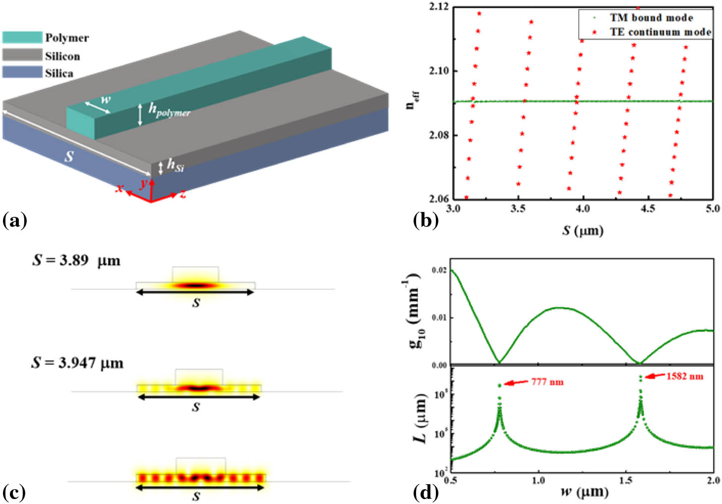
    Fig. 1. Conventional BIC waveguide. (a) Schematic of the BIC waveguide. (b) Effective mode indices of the TM bound mode and the TE continuum modes with varying substrate width S. (c) Field distributions under different S. (d) Upper panel: solved coupling strength g10 as a function of waveguide width w. Lower panel: propagation distance L at various waveguide widths w with infinite S. Red arrows indicate the maximum values.
    BIC in dual waveguide configuration. (a) Schematic of BICs consists of two waveguides with interval d. The widths are defined as w1 and w2, respectively. (b) Loss channels formed by energy leaking from the TM bound mode to the TE continuum mode.
    Fig. 2. BIC in dual waveguide configuration. (a) Schematic of BICs consists of two waveguides with interval d. The widths are defined as w1 and w2, respectively. (b) Loss channels formed by energy leaking from the TM bound mode to the TE continuum mode.
    Numerically calculated coupling strength for dual BICs waveguides. (a) Effective indices of the symmetric TM bound modes (olive circles), antisymmetric TM bound modes (blue empty circles), and TE continuum modes (red stars) as a function of the silicon substrate width S. (b) Electric field distributions of the modes marked in (a). (c) Coupling strength g14 (upper panel) and propagation length L (lower panel) against waveguide interval d, respectively. (d) Electric field distribution of the dual waveguide system along propagation direction with w=1.1 μm and d=0.852 μm for infinite S.
    Fig. 3. Numerically calculated coupling strength for dual BICs waveguides. (a) Effective indices of the symmetric TM bound modes (olive circles), antisymmetric TM bound modes (blue empty circles), and TE continuum modes (red stars) as a function of the silicon substrate width S. (b) Electric field distributions of the modes marked in (a). (c) Coupling strength g14 (upper panel) and propagation length L (lower panel) against waveguide interval d, respectively. (d) Electric field distribution of the dual waveguide system along propagation direction with w=1.1  μm and d=0.852  μm for infinite S.
    Propagation distance under varied waveguide gaps d. The waveguide width from 1 to 1.5 μm is selected to explore the BICs established in the dual waveguide architecture.
    Fig. 4. Propagation distance under varied waveguide gaps d. The waveguide width from 1 to 1.5 μm is selected to explore the BICs established in the dual waveguide architecture.
    Cladding-layer-covered dual waveguide system. (a) Schematic of the dual waveguide system with a cladding layer. (b)–(f) Propagation length L as a function of waveguide intervals d with nc=1.1, 1.2, 1.3, 1.4, and 1.45, respectively. The width range between black arrows is defined as Δd. (g) Width range Δd against nc.
    Fig. 5. Cladding-layer-covered dual waveguide system. (a) Schematic of the dual waveguide system with a cladding layer. (b)–(f) Propagation length L as a function of waveguide intervals d with nc=1.1, 1.2, 1.3, 1.4, and 1.45, respectively. The width range between black arrows is defined as Δd. (g) Width range Δd against nc.
    BIC in dual waveguide system with cladding layer. (a) Coupling strength g14 against waveguide interval d. Here, the waveguide width is w1=w2=w=1.1 μm and nc=1.45. (b) Tendency of propagation length with the width w2 of the dual waveguide system. Here, w1 is fixed as 1.1 μm.
    Fig. 6. BIC in dual waveguide system with cladding layer. (a) Coupling strength g14 against waveguide interval d. Here, the waveguide width is w1=w2=w=1.1  μm and nc=1.45. (b) Tendency of propagation length with the width w2 of the dual waveguide system. Here, w1 is fixed as 1.1 μm.
    Fabrication tolerance of (a) the dual waveguide system and (b) the single waveguide system.
    Fig. 7. Fabrication tolerance of (a) the dual waveguide system and (b) the single waveguide system.
    Zhiyuan Gu, Sen Jiang, Chang Liu, Nan Zhang, "Robust bound states in the continuum in a dual waveguide system," Photonics Res. 11, 575 (2023)
    Download Citation