• Photonics Research
  • Vol. 9, Issue 10, 2024 (2021)
Langlang Xiong1、2, Yu Zhang1、2、3, and Xunya Jiang1、2、3、*
Author Affiliations
  • 1Institute of Future Lighting, Academy for Engineering and Technology, Fudan University, Shanghai 200433, China
  • 2Engineering Research Center of Advanced Lighting Technology, Fudan University, Ministry of Education, Shanghai 200433, China
  • 3Department of Illuminating Engineering and Light Sources, School of Information Science and Engineering, Fudan University, Shanghai 200433, China
  • show less
    DOI: 10.1364/PRJ.423260 Cite this Article Set citation alerts
    Langlang Xiong, Yu Zhang, Xunya Jiang. Resonance and topological singularity near and beyond zero frequency for waves: model, theory, and effects[J]. Photonics Research, 2021, 9(10): 2024 Copy Citation Text show less
    Abstract model that could have near-zero frequency resonance, which can be regarded as a virtual interface embedded at the center of the FP cavity.
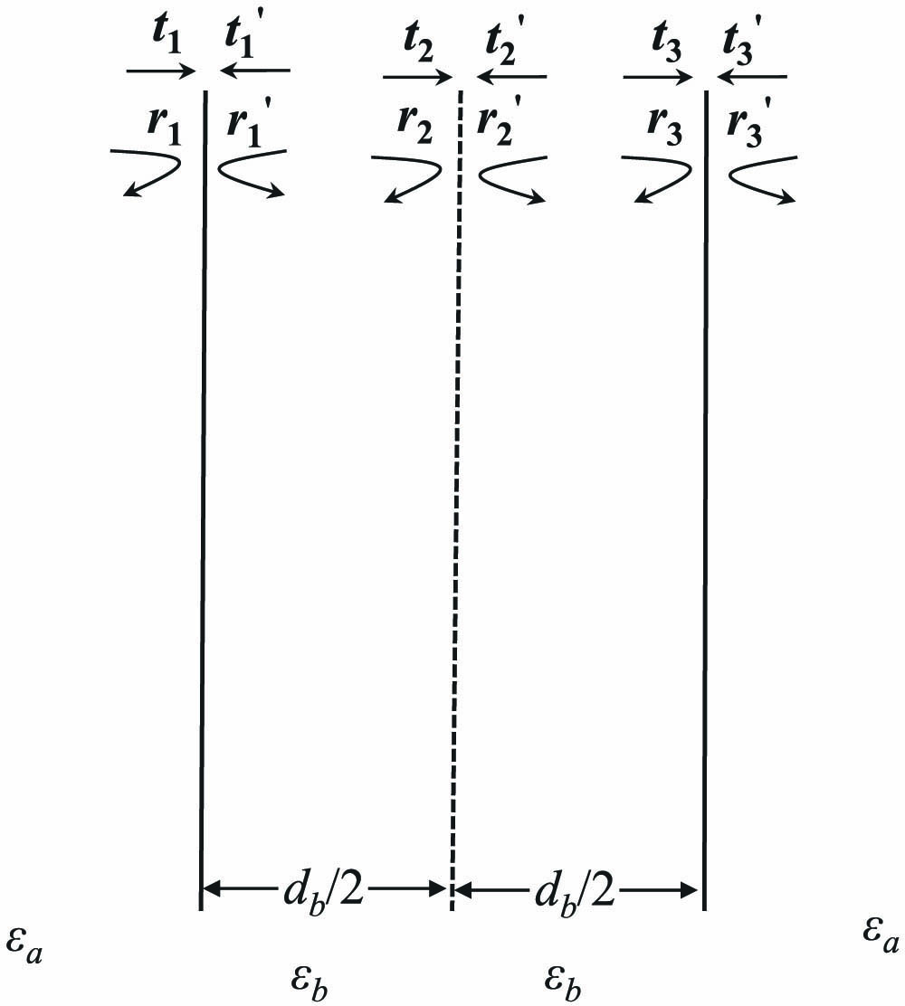
    Fig. 1. Abstract model that could have near-zero frequency resonance, which can be regarded as a virtual interface embedded at the center of the FP cavity.
    Physical realizations of the resonator with near-zero frequency resonance. (a) General realization with two partial reflectors and a side-coupled or embedded subresonator; (b) physical realization of a side-coupled stub waveguide; (c) physical realization of a layered structure with an embedded FP cavity.
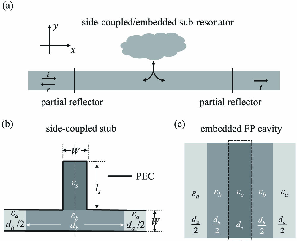
    Fig. 2. Physical realizations of the resonator with near-zero frequency resonance. (a) General realization with two partial reflectors and a side-coupled or embedded subresonator; (b) physical realization of a side-coupled stub waveguide; (c) physical realization of a layered structure with an embedded FP cavity.
    Resonant frequencies versus the stub length ls with da=0.5 mm, db=1 mm, εa=4, εb=εs=6.25, and μa=μb=μs=1. The black solid line represents the calculated result of TMM, and the blue square, red circles, and green line with asterisks represent the result of FEM with different widths of waveguide and stub W=1 μm, 5 μm, and 100 μm, respectively. The result of silver substrate with W=100 μm is plotted as cyan diamonds.
    Fig. 3. Resonant frequencies versus the stub length ls with da=0.5  mm, db=1  mm, εa=4, εb=εs=6.25, and μa=μb=μs=1. The black solid line represents the calculated result of TMM, and the blue square, red circles, and green line with asterisks represent the result of FEM with different widths of waveguide and stub W=1  μm, 5 μm, and 100 μm, respectively. The result of silver substrate with W=100  μm is plotted as cyan diamonds.
    Periodic arrangement of the structure in Section 3. We set the distance Δ from the center of the stub to the center of layer-A as a free parameter, also known as synthetic dimension.
    Fig. 4. Periodic arrangement of the structure in Section 3. We set the distance Δ from the center of the stub to the center of layer-A as a free parameter, also known as synthetic dimension.
    Reflection phase and reflectivity projection band diagram at the synthetic dimension Δ/a and frequency.
    Fig. 5. Reflection phase and reflectivity projection band diagram at the synthetic dimension Δ/a and frequency.
    Reflection coefficient for four kinds of finite PhCs with N=10 cells. The first, second, and third bands are marked as B1, B2, and B3, respectively. (a) PhC-A, da=1.35 mm, db=0.75 mm, εa=4, εb=εs=6.25, and ls=0 mm; (b) PhC-B, da=1.05 mm, db=1 mm, εa=4, εb=εs=6.25, and ls=0 mm; (c) PhC-C, da=0.8 mm, db=1 mm, εa=4, εb=εs=6.25, and ls=lc=db(εb−εa)/εa=0.563 mm; (d) PhC-D, da=1 mm, db=1 mm, εa=4, εb=εs=6.25, and ls=0.6 mm>lc.
    Fig. 6. Reflection coefficient for four kinds of finite PhCs with N=10 cells. The first, second, and third bands are marked as B1, B2, and B3, respectively. (a) PhC-A, da=1.35  mm, db=0.75  mm, εa=4, εb=εs=6.25, and ls=0  mm; (b) PhC-B, da=1.05  mm, db=1  mm, εa=4, εb=εs=6.25, and ls=0  mm; (c) PhC-C, da=0.8  mm, db=1  mm, εa=4, εb=εs=6.25, and ls=lc=db(εbεa)/εa=0.563  mm; (d) PhC-D, da=1  mm, db=1  mm, εa=4, εb=εs=6.25, and ls=0.6  mm>lc.
    Reflection coefficient and magnetic field of the edge state. (a) Splice PhC-A (5 cells) with PhC-B (10 cells); (b) splice PhC-C (5 cells) with PhC-B (10 cells); (c) splice PhC-D (5 cells) with PhC-B (10 cells).
    Fig. 7. Reflection coefficient and magnetic field of the edge state. (a) Splice PhC-A (5 cells) with PhC-B (10 cells); (b) splice PhC-C (5 cells) with PhC-B (10 cells); (c) splice PhC-D (5 cells) with PhC-B (10 cells).
    Trajectory of singularity in space {fr,fi,ls}.
    Fig. 8. Trajectory of singularity in space {fr,fi,ls}.
    (a) Black dashed line, the trajectory of singularity in space {dc,f}; parameters are set as da=db=1 mm, εa=4, εb=1.5, and εc=9; color map, reflectivity of layered structure in space {dc,f} with loss and randomness; parameters are set as ε^m=εm+0.003iεm, d^m=dm(1+W·γ), where m=a,b,c, W=0.01 is random strength, γ is an evenly distributed random number in the range [−1,1]; (b) reflection coefficient of PhC-E with da=1.4 mm, db=1 mm, dc=0.2 mm, εa=4, εb=1.5, εc=9, and N=10; (c) reflection coefficient of PhC-F with da=1 mm, db=1 mm, dc=dc0=0.5 mm, εa=4, εb=1.5, εc=9, and N=10; (d) reflection coefficient of PhC-G with da=1.2 mm, db=1 mm, dc=0.55 mm>dc0, εa=4, εb=1.5, εc=9, and N=10; (e) reflection coefficient and electric field of the edge state by splicing PhC-F (5 cells) with PhC-E (15 cells); (f) reflection coefficient and electric field of the edge state by splicing PhC-G (5 cells) with PhC-E (15 cells).
    Fig. 9. (a) Black dashed line, the trajectory of singularity in space {dc,f}; parameters are set as da=db=1  mm, εa=4, εb=1.5, and εc=9; color map, reflectivity of layered structure in space {dc,f} with loss and randomness; parameters are set as ε^m=εm+0.003iεm, d^m=dm(1+W·γ), where m=a,b,c, W=0.01 is random strength, γ is an evenly distributed random number in the range [1,1]; (b) reflection coefficient of PhC-E with da=1.4  mm, db=1  mm, dc=0.2  mm, εa=4, εb=1.5, εc=9, and N=10; (c) reflection coefficient of PhC-F with da=1  mm, db=1  mm, dc=dc0=0.5  mm, εa=4, εb=1.5, εc=9, and N=10; (d) reflection coefficient of PhC-G with da=1.2  mm, db=1  mm, dc=0.55  mm>dc0, εa=4, εb=1.5, εc=9, and N=10; (e) reflection coefficient and electric field of the edge state by splicing PhC-F (5 cells) with PhC-E (15 cells); (f) reflection coefficient and electric field of the edge state by splicing PhC-G (5 cells) with PhC-E (15 cells).
    WFFB with da=db=1 mm, εa=4, εb=1.5, and εc=9. (a) Real part of WFFB with dc=0.2 mm; (b) real part of WFFB with dc=0.35 mm; (c) imaginary part of WFFB with dc=0.35 mm; (d) real part of WFFB with dc=0.49 mm; (e) imaginary part of WFFB with dc=0.49 mm; (f) imaginary part (black line) and real part (red line) of WFFB with dc=0.5 mm; (g) imaginary part of WFFB with dc=0.6 mm.
    Fig. 10. WFFB with da=db=1  mm, εa=4, εb=1.5, and εc=9. (a) Real part of WFFB with dc=0.2  mm; (b) real part of WFFB with dc=0.35  mm; (c) imaginary part of WFFB with dc=0.35  mm; (d) real part of WFFB with dc=0.49  mm; (e) imaginary part of WFFB with dc=0.49  mm; (f) imaginary part (black line) and real part (red line) of WFFB with dc=0.5  mm; (g) imaginary part of WFFB with dc=0.6  mm.
    Reflectivity of periodic structure with εa=16+3i, εb=9+1i, εc=25+8i, da=db=0.8 mm, and N=10. The black dotted-dashed line, black solid line, and black dashed line represent dc=0.4 mm, 0.5 mm, and 0.6 mm, respectively.
    Fig. 11. Reflectivity of periodic structure with εa=16+3i, εb=9+1i, εc=25+8i, da=db=0.8  mm, and N=10. The black dotted-dashed line, black solid line, and black dashed line represent dc=0.4  mm, 0.5 mm, and 0.6 mm, respectively.
    (a) Type A, which represents the direct reflection of incident wave by interface 1 (r1); (b) type B, which represents the coupled reflection between interface 1 (r1′) and interface 2 (r2) or interface 2 (r2′) and interface 3 (r3); (c) type C, which represents the coupled reflection between interface 1 (r1′) and interface 3 (r3); (d) type D, all other possible paths that include the coupled reflection from all three interfaces.
    Fig. 12. (a) Type A, which represents the direct reflection of incident wave by interface 1 (r1); (b) type B, which represents the coupled reflection between interface 1 (r1) and interface 2 (r2) or interface 2 (r2) and interface 3 (r3); (c) type C, which represents the coupled reflection between interface 1 (r1) and interface 3 (r3); (d) type D, all other possible paths that include the coupled reflection from all three interfaces.
    Results of TMM (solid line) and Eq. (B5) (asterisk) with da=db=1 mm, εa=4, εb=εs=6.25, and ls=db(εb−εa)/εa=0.563 mm.
    Fig. 13. Results of TMM (solid line) and Eq. (B5) (asterisk) with da=db=1  mm, εa=4, εb=εs=6.25, and ls=db(εbεa)/εa=0.563  mm.
    GapPhC-APhC-BPhC-CPhC-D
    First gap<0<0>0>0
    Second gap>0<0<0<0
    Table 1. Sign of ς for Different PhCs and Different Gaps
    Langlang Xiong, Yu Zhang, Xunya Jiang. Resonance and topological singularity near and beyond zero frequency for waves: model, theory, and effects[J]. Photonics Research, 2021, 9(10): 2024
    Download Citation