• Journal of Infrared and Millimeter Waves
  • Vol. 40, Issue 6, 732 (2021)
Hui-Lin HUANG, Jing HUANG, and Quan SHI*
Author Affiliations
  • School of Information Science and Technology,Nantong University,Nantong 226019,China
  • show less
    DOI: 10.11972/j.issn.1001-9014.2021.06.005 Cite this Article
    Hui-Lin HUANG, Jing HUANG, Quan SHI. A parameter extraction method of the Schottky diode millimeter wave equivalent circuit model[J]. Journal of Infrared and Millimeter Waves, 2021, 40(6): 732 Copy Citation Text show less
    (a)Cross-section of Schottky diode,(b)equivalent-circuit model
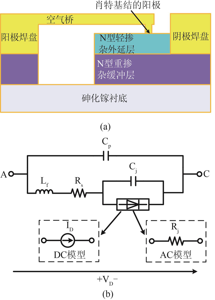
    Fig. 1. (a)Cross-section of Schottky diode,(b)equivalent-circuit model
    Layouts of test structure (a)open, (b)short
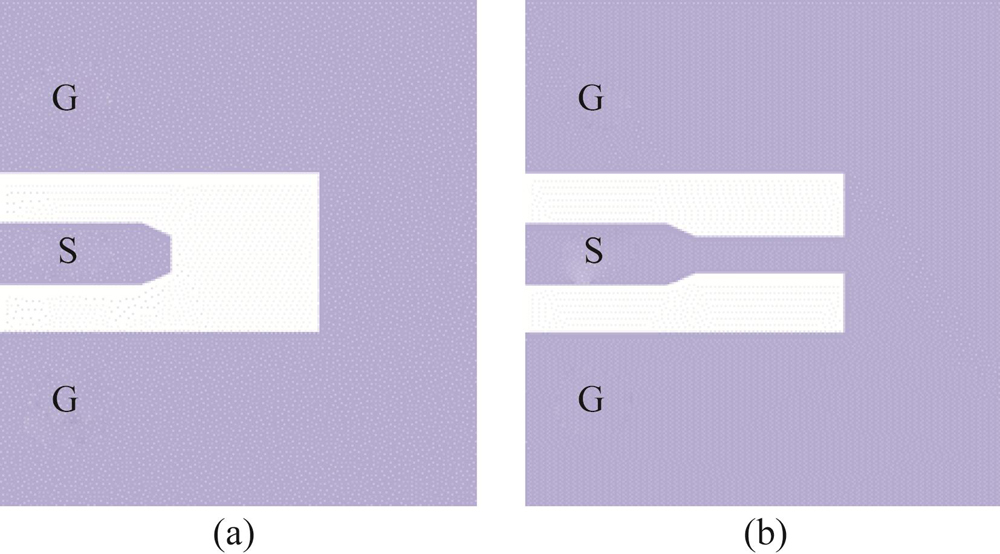
    Fig. 2. Layouts of test structure (a)open, (b)short
    Equivalent circuit models of test structure (a)open, (b)short
    Fig. 3. Equivalent circuit models of test structure (a)open, (b)short
    Layouts of test structure
    Fig. 4. Layouts of test structure
    Equivalent circuit model under Schottky diode forward bias condition
    Fig. 5. Equivalent circuit model under Schottky diode forward bias condition
    Equivalent circuit model under Schottky diode reversed bias condition
    Fig. 6. Equivalent circuit model under Schottky diode reversed bias condition
    Parasitic elements versus frequency in 1~40 GHz frequency range (a)pad capacitance Cp, (b)feedline inductanceLf
    Fig. 7. Parasitic elements versus frequency in 1~40 GHz frequency range (a)pad capacitance Cp, (b)feedline inductanceLf
    ln(ID)versus VD
    Fig. 8. ln(ID)versus VD
    Total resistance Rt versus the bias voltage VD
    Fig. 9. Total resistance Rt versus the bias voltage VD
    Intrinsic elements versus the bias voltage VD (a)junction capacitance Cj, (b)junction resistance Rj
    Fig. 10. Intrinsic elements versus the bias voltage VD (a)junction capacitance Cj, (b)junction resistance Rj
    Comparison of modeled and measured IDversus VD
    Fig. 11. Comparison of modeled and measured IDversus VD
    Comparison of modeled and measured data of Schottky diode (a)real part of S11 under reversed bias condition,(b)imaginary part of S11 under reversed bias condition,(c)real part of S11 under forward bias condition,(d)imaginary part of S11 under forward bias condition
    Fig. 12. Comparison of modeled and measured data of Schottky diode (a)real part of S11 under reversed bias condition,(b)imaginary part of S11 under reversed bias condition,(c)real part of S11 under forward bias condition,(d)imaginary part of S11 under forward bias condition
    Relative error of S11 versus frequency
    Fig. 13. Relative error of S11 versus frequency
    参数数值参数数值
    Is/A1.44×10-14Vbi/V0.68
    n1.15m0.503
    Rs()6.48Cp/fF14.73
    Rs ()7.09Lf/pH27.46
    Cj0/fF24.21
    Table 1. Extracted the model parameters of Schottky diode
    Hui-Lin HUANG, Jing HUANG, Quan SHI. A parameter extraction method of the Schottky diode millimeter wave equivalent circuit model[J]. Journal of Infrared and Millimeter Waves, 2021, 40(6): 732
    Download Citation