• Photonics Research
  • Vol. 6, Issue 4, 277 (2018)
Qian Gao, Erwen Li, and Alan X. Wang*
Author Affiliations
  • School of Electrical Engineering and Computer Science, Oregon State University, Corvallis, Oregon 97331, USA
  • show less
    DOI: 10.1364/PRJ.6.000277 Cite this Article Set citation alerts
    Qian Gao, Erwen Li, Alan X. Wang. Ultra-compact and broadband electro-absorption modulator using an epsilon-near-zero conductive oxide[J]. Photonics Research, 2018, 6(4): 277 Copy Citation Text show less
    (a) 3D Schematic of the plasmonic EA modulator. (b) Enlarged view of the cross-sectional area of the active E-O modulation region and (c) enlarged view of the Au slot waveguide with tapers to silicon waveguides.
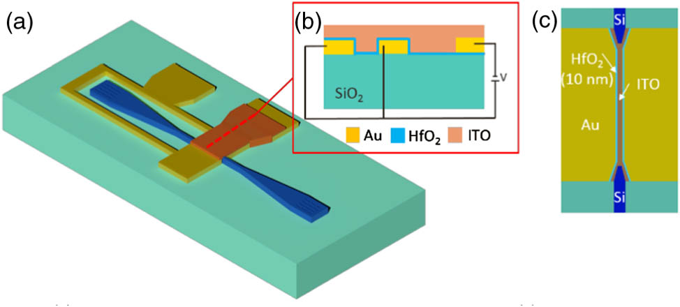
    Fig. 1. (a) 3D Schematic of the plasmonic EA modulator. (b) Enlarged view of the cross-sectional area of the active E-O modulation region and (c) enlarged view of the Au slot waveguide with tapers to silicon waveguides.
    Simulated optical mode profiles for (a) the plasmonic slot waveguide with Np=Nb=1×1020 cm−3 and (b) the plasmonic slot waveguide with ITO at ENZ when Np=7.5×1020 cm−3. The inset shows the enlarged region with the ENZ ITO layer. Top view of optical field distributions at (c) the ON state (accumulation layer Nb=Np=1×1020 cm−3) and (d) the OFF state (accumulation layer Np=7.5×1020 cm−3). The optical field profile is plotted in log scale. (e) The propagation loss of the plasmonic slot waveguide at different peak carrier concentrations. (f) Transmission at the ON state and OFF state and the extinction ratio as a function of the optical wavelength.
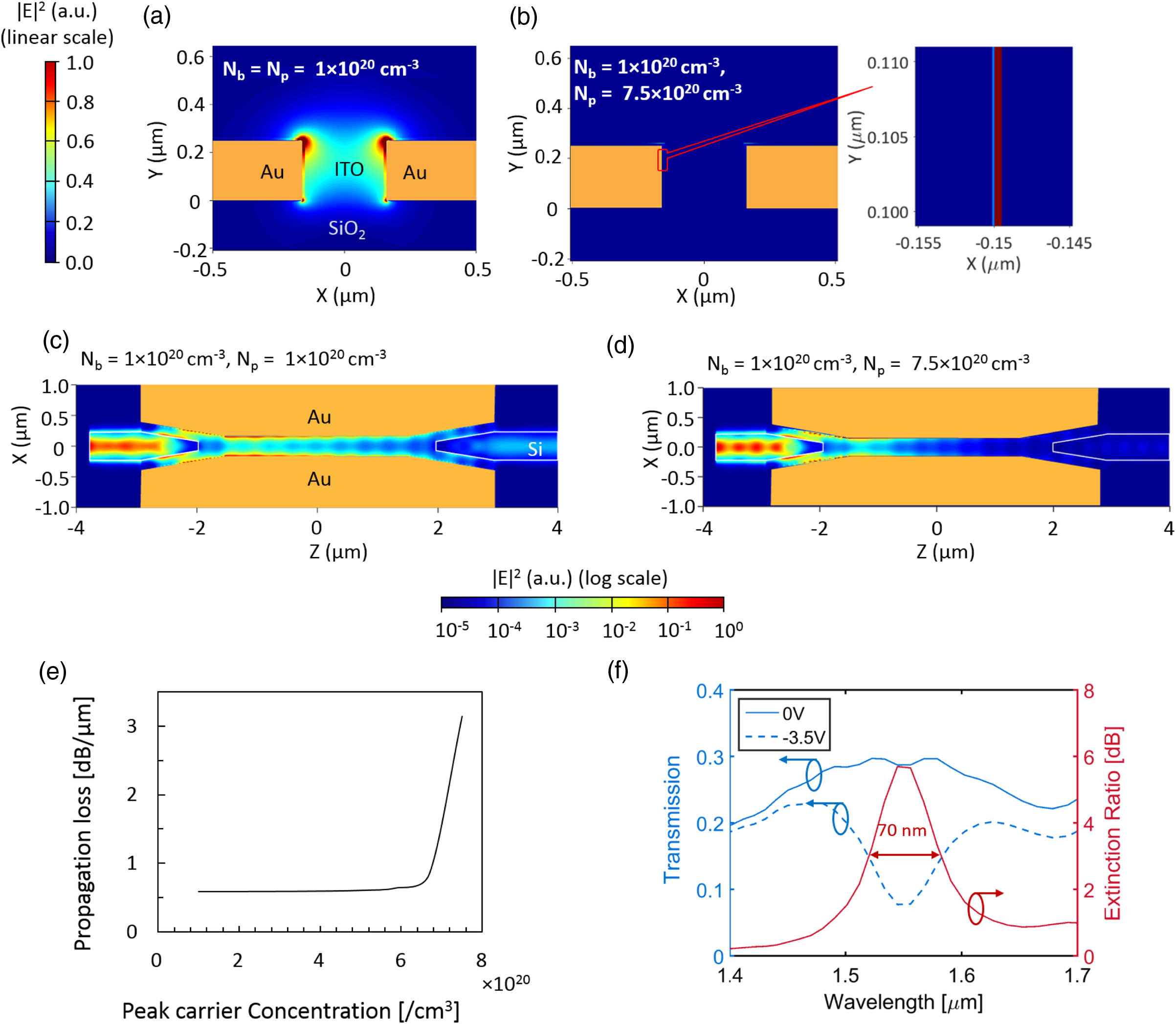
    Fig. 2. Simulated optical mode profiles for (a) the plasmonic slot waveguide with Np=Nb=1×10²⁰  cm3 and (b) the plasmonic slot waveguide with ITO at ENZ when Np=7.5×10²⁰  cm3. The inset shows the enlarged region with the ENZ ITO layer. Top view of optical field distributions at (c) the ON state (accumulation layer Nb=Np=1×10²⁰  cm3) and (d) the OFF state (accumulation layer Np=7.5×10²⁰  cm3). The optical field profile is plotted in log scale. (e) The propagation loss of the plasmonic slot waveguide at different peak carrier concentrations. (f) Transmission at the ON state and OFF state and the extinction ratio as a function of the optical wavelength.
    (a) Optical image of the plasmonic slot waveguide integrated with Si waveguides. (b) SEM image of the plasmonic slot waveguide. (c) Enlarged SEM image of the tapered region. (d) SEM image of the cross-sectional view of the slot waveguide.
    Fig. 3. (a) Optical image of the plasmonic slot waveguide integrated with Si waveguides. (b) SEM image of the plasmonic slot waveguide. (c) Enlarged SEM image of the tapered region. (d) SEM image of the cross-sectional view of the slot waveguide.
    (a) Change of the measured (blue) and simulated (red) transmission with the applied gate voltage. (b) Left: measured static transmission spectra with no applied bias and 3.5 V bias. Right: measured ER with 3.5 V applied bias.
    Fig. 4. (a) Change of the measured (blue) and simulated (red) transmission with the applied gate voltage. (b) Left: measured static transmission spectra with no applied bias and 3.5 V bias. Right: measured ER with 3.5 V applied bias.
    Dynamic optical modulation testing results with −2 to 2 V sweep input bias voltage at 40 MHz.
    Fig. 5. Dynamic optical modulation testing results with 2 to 2 V sweep input bias voltage at 40 MHz.
    Qian Gao, Erwen Li, Alan X. Wang. Ultra-compact and broadband electro-absorption modulator using an epsilon-near-zero conductive oxide[J]. Photonics Research, 2018, 6(4): 277
    Download Citation