• Photonics Research
  • Vol. 8, Issue 8, 1368 (2020)
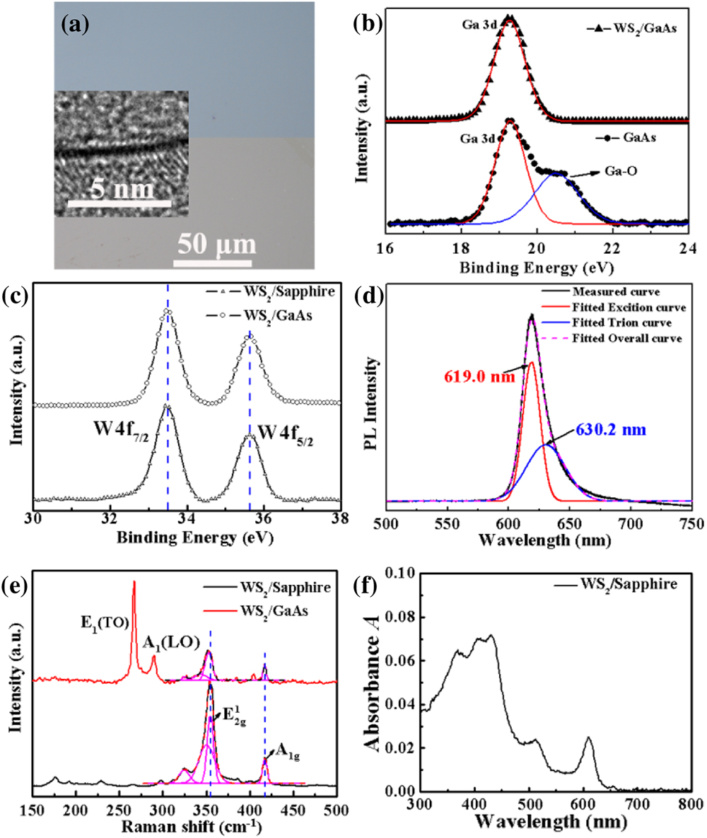
Kuilong Li1、3、*, Wenjia Wang1、4、*, Jianfei Li1, Wenxin Jiang1, Min Feng1, and Yang He2
Author Affiliations
  • 1School of Electronic and Information Engineering (Department of Physics), Qilu University of Technology (Shandong Academy of Sciences),Jinan 250353, China
  • 2Institute of Electronic and Electrical, Changzhou College of Information Technology, Changzhou 213164, China
  • 3e-mail: likuilong123@126.com
  • 4e-mail: wangwenjia87@sina.com
  • show less
    DOI: 10.1364/PRJ.396880 Cite this Article Set citation alerts
    Kuilong Li, Wenjia Wang, Jianfei Li, Wenxin Jiang, Min Feng, Yang He. High-responsivity, self-driven photodetectors based on monolayer WS2/GaAs heterojunction[J]. Photonics Research, 2020, 8(8): 1368 Copy Citation Text show less
    (a) Optical images of the WS2/sapphire sample (bottom) and WS2/GaAs sample (top). The inset image corresponds to the cross-sectional TEM result of WS2/sapphire. (b) The X ray photoelectron spectroscopy obtained from the uncleaned GaAs substrate and WS2/GaAs sample. (c) The W 4f spectrum of the WS2/sapphire and WS2/GaAs samples. (d) The room temperature photoluminescence spectrum of the monolayer WS2 grown on sapphire substrate, and the related fitted exciton and trion peaks. (e) Raman spectra of both monolayer WS2/sapphire and monolayer WS2/GaAs samples. (f) The absorbance spectrum of monolayer WS2 grown on sapphire substrate.
    Fig. 1. (a) Optical images of the WS2/sapphire sample (bottom) and WS2/GaAs sample (top). The inset image corresponds to the cross-sectional TEM result of WS2/sapphire. (b) The X ray photoelectron spectroscopy obtained from the uncleaned GaAs substrate and WS2/GaAs sample. (c) The W 4f spectrum of the WS2/sapphire and WS2/GaAs samples. (d) The room temperature photoluminescence spectrum of the monolayer WS2 grown on sapphire substrate, and the related fitted exciton and trion peaks. (e) Raman spectra of both monolayer WS2/sapphire and monolayer WS2/GaAs samples. (f) The absorbance spectrum of monolayer WS2 grown on sapphire substrate.
    (a) Schematic structure of the WS2/GaAs photodetector, and the insets are the optical microscopy images of the device arrays (left) and single device (right). (b) Dark and light I–V curves of the GaAs photodetector (left) and WS2/GaAs photodetector (right) under different wavelength light illumination (365 nm, 460 nm, 660 nm, and 880 nm). (c) Schematic band diagrams at the interface of the WS2/GaAs heterojunction.
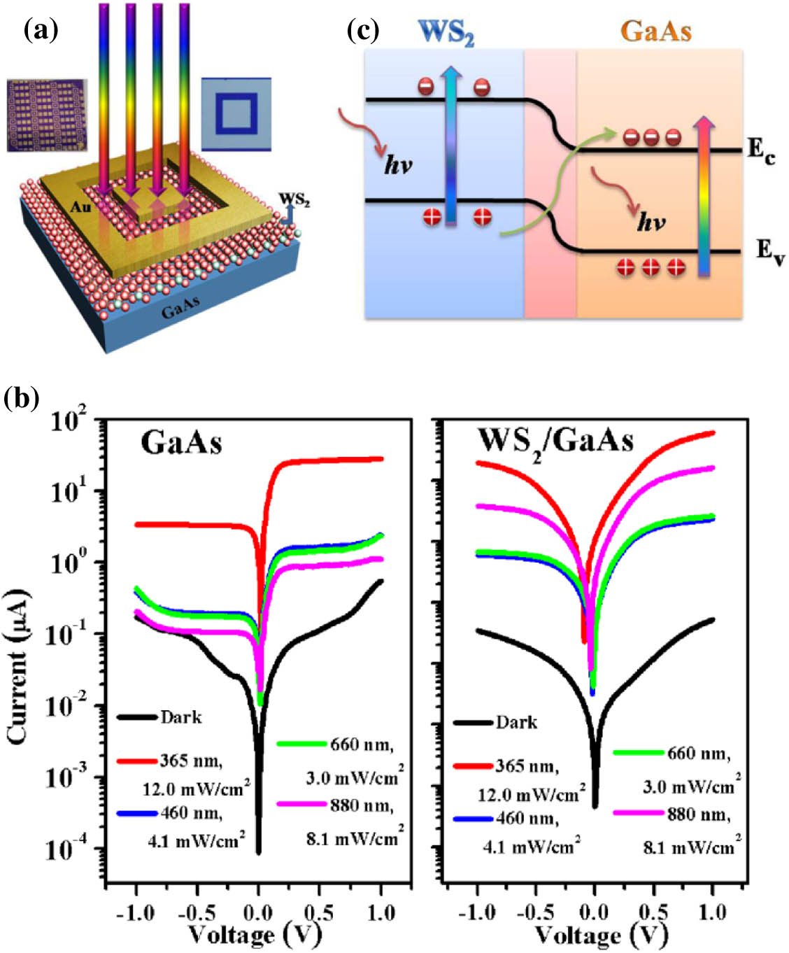
    Fig. 2. (a) Schematic structure of the WS2/GaAs photodetector, and the insets are the optical microscopy images of the device arrays (left) and single device (right). (b) Dark and light I–V curves of the GaAs photodetector (left) and WS2/GaAs photodetector (right) under different wavelength light illumination (365 nm, 460 nm, 660 nm, and 880 nm). (c) Schematic band diagrams at the interface of the WS2/GaAs heterojunction.
    (a) and (b) show the dark and light I–V curves at 365 nm illumination under different incident light power of the GaAs and WS2/GaAs photodetectors, respectively. (c) and (d) are the photocurrent as a function of incident light power under 365 nm at a fixed voltage of 1.0 V for the GaAs and WS2/GaAs photodetectors, respectively. (e) and (f) are the corresponding photoresponsivity according to the photocurrent obtained above.
    Fig. 3. (a) and (b) show the dark and light I–V curves at 365 nm illumination under different incident light power of the GaAs and WS2/GaAs photodetectors, respectively. (c) and (d) are the photocurrent as a function of incident light power under 365 nm at a fixed voltage of 1.0 V for the GaAs and WS2/GaAs photodetectors, respectively. (e) and (f) are the corresponding photoresponsivity according to the photocurrent obtained above.
    (a) Exhibits the dark and light I–V curves under 880 nm illumination with different incident light power of the WS2/GaAs photodetectors. (b) shows the corresponding photocurrent and photoresponsivity. (c) displays the dark and light I–V curves under 460 nm illumination with different incident light power of the WS2/GaAs photodetectors. (d) shows the corresponding photocurrent and photoresponsivity.
    Fig. 4. (a) Exhibits the dark and light I–V curves under 880 nm illumination with different incident light power of the WS2/GaAs photodetectors. (b) shows the corresponding photocurrent and photoresponsivity. (c) displays the dark and light I–V curves under 460 nm illumination with different incident light power of the WS2/GaAs photodetectors. (d) shows the corresponding photocurrent and photoresponsivity.
    (a) and (b) are the noise equivalent power (NEP) and normalized detectivity D* of both GaAs and WS2/GaAs photodetectors as a function of incident power, respectively.
    Fig. 5. (a) and (b) are the noise equivalent power (NEP) and normalized detectivity D* of both GaAs and WS2/GaAs photodetectors as a function of incident power, respectively.
    (a) and (c) are the photocurrent-time curves of WS2/GaAs photodetector at −1 V illuminated by 365 nm and 880 nm light, respectively. Meanwhile, the performance of the device under 365 nm after three days was also shown. (b) and (d) are the determined rise time (from 10% to 90% of maximum photocurrent) and fall time (from 90% to 10% of maximum photocurrent) of the detector under 365 nm and 880 nm light, respectively.
    Fig. 6. (a) and (c) are the photocurrent-time curves of WS2/GaAs photodetector at 1  V illuminated by 365 nm and 880 nm light, respectively. Meanwhile, the performance of the device under 365 nm after three days was also shown. (b) and (d) are the determined rise time (from 10% to 90% of maximum photocurrent) and fall time (from 90% to 10% of maximum photocurrent) of the detector under 365 nm and 880 nm light, respectively.
    Kuilong Li, Wenjia Wang, Jianfei Li, Wenxin Jiang, Min Feng, Yang He. High-responsivity, self-driven photodetectors based on monolayer WS2/GaAs heterojunction[J]. Photonics Research, 2020, 8(8): 1368
    Download Citation