Abstract
Constructing two-dimensional (2D) layered materials with traditional three-dimensional (3D) semiconductors into complex heterostructures has opened a new platform for the development of optoelectronic devices. Herein, large-area high performance self-driven photodetectors based on monolayer heterostructures were successfully fabricated with a wide response spectrum band ranging from the ultraviolet to near-infrared region. The detector exhibits an overall high performance, including high photoresponsivity of 65.58 A/W at 365 nm and 28.50 A/W at 880 nm, low noise equivalent power of , high detectivity of , and fast response speed of 30/10 ms. This work suggests that the heterostructure is promising in future novel optoelectronic device applications, and also provides a low-cost, easy-to-process method for the preparation of 2D/3D heterojunction-based devices.1. INTRODUCTION
The capabilities of modern optoelectronic and electronic devices have been broadened extensively since the emergence of two-dimensional (2D) layered materials [1–4]. In comparison with traditional three-dimensional (3D) bulk semiconductors, the unprecedented properties of 2D materials include a tunable layer-dependent energy bandgap, dangling bond-free surface, excellent bending durability, strong light–matter coupling, and outstanding integrating compatibility [5–8]. Transition metal dichalcogenides (TMDCs), such as , , and , as an important member of 2D material family, have drawn tremendous research interest and have been widely employed in the fields of photodetectors, transistors, sensors, and new energy devices [9–12]. Among them, monolayer with a direct energy bandgap about 2.0 eV and high photo-emission quantum yields () has been intensively studied in photodetection applications [13]. Yao et al. first demonstrated a multilayer -based photodetector, which exhibits a high responsivity of 0.51 A/W, high carrier mobility of , and broadband response [14]. The photoresponsivity of the lateral graphene–monolayer –graphene photodetector reaches 3.5 A/W under illumination power density of with graphene as 2D electrode [15]. Lan et al. reported wafer-scale and homogeneous monolayer photodetectors grown by enhanced chemical vapor deposition (CVD) with a responsivity of , a detectivity of , and a fast response speed () [16]. Normally, photoresponsivity as a figure of merit for photodetectors is slow in pure 2D material-based photodetectors owing to their limited thickness and poor optical absorbance. In addition, their response spectrum is also usually narrow, which is restricted by their bandgap. A plasmon resonance enhanced photodetector employing Au nanospheres at the surface has reach an excellent high responsivity of 1050 A/W at the wavelength of 590 nm with the help of localized surface plasmon resonance (LSPR) [17]. Another promising way to improve the responsivity and extend the response spectrum profoundly is to form hybrid structures with other semiconductors such as 1D/2D, 2D/2D, and 2D/3D heterojunctions [18]. Specially, 3D semiconductors (e.g., GaAs, Si, InP, GaN, and Ge) have been used in commercial photodetectors. However, their further development is seriously hindered by the lattice mismatch through introducing dislocations and defects at the interface, which is detrimental to the devices. Therefore, it is believed that the conjunction of 2D and 3D semiconductors can bring about new vitality for both 2D- and 3D-related semiconductor devices.
Until now, 2D/3D heterojunction optoelectronic devices have achieved certain progresses. Black phosphorus/GaAs p-n heterojunctions exhibit close-to-ideal diode behavior at low bias, while under illumination they display a photo-response with an external quantum efficiency of up to 10% at zero bias [19]. The monolayer heterostructure self-driven photodetector exhibits high sensitivity to the incident light of 635 nm with responsivity and detectivity as high as and , respectively [20]. Kim et al. designed a heterojunction photodetector, which is sensitive to light ranging from ultraviolet (UV) to near-infrared spectrum with an ultrafast response speed of 1.1 μs [21]. A type of broadband (325–980 nm) self-powered photodetector based on graphene/GaAs van der Waals heterojunction has also been reported by Lu et al. [22]. In addition, in our previous report, monolayer heterostructures were successfully fabricated, and a type-II band alignment at the interface was verified using X-ray photoelectron spectroscopy (XPS) and ultraviolet photoelectron spectroscopy (UPS) technology [23]. For photodetectors, the heterostructures with type-II band alignment cannot only extend the response spectrum range by breaking the limitation of the intrinsic bandgaps of the component materials, but also can stimulate carrier separation by the aid of a built-in electric field. This is quite fascinating for the design of broadband self-driven photodetectors.
In this paper, we constructed a simple and high performance self-driven broadband photodetector by transferring monolayer onto n-type GaAs, which can detect photons from UV to near-infrared light. The photoresponsivity of the photodetector at 365 nm and 880 nm reaches 65.58 A/W and 28.50 A/W, respectively. Meanwhile, the detectivity under 365 nm illumination is as high as , about 1 order of magnitude higher than the corresponding value of the GaAs photodetector. Besides those, photo-response switching characteristics were also explored, which prove the superiority of the photodetector to other -related and 2D/3D heterojunction-based photodetectors.
Sign up for Photonics Research TOC. Get the latest issue of Photonics Research delivered right to you!Sign up now
2. METHOD
A. Sample Preparation and Device Fabrication
In this paper, the investigated large-area (over ) monolayer films were grown on sapphire substrates using CVD technology with powder and sulfur flakes as sources and Ar gas as the carrier gas. The quartz tube was first purged by Ar gas to bring down the air concentration as much as possible before the growth process. Then, the substrate was gradually heated to about 850°C, which corresponds to the sulfurization temperature, and the sulfur temperature was maintained at 200°C for 13 min to supply sulfur precursor. After this, the prepared monolayer was transferred onto (001) oriented Si-doped n-type GaAs substrates with doping density about by the mature PMMA method [24]. Before the transfer process, GaAs substrates were first cleaned utilizing acetone and isopropanol reagent by the aid of ultrasonic processing and washed thoroughly with deionized water to remove grease. Subsequently, the surface oxide was removed using hydrochloric acid, and eventually, the substrates were washed using deionized water and dried by . Ti (5 nm)/Au (50 nm) and Au (50 nm) were selected as the electrode and deposited on monolayer- and GaAs, respectively, through UV lithography, e-beam evaporation, and lift-off processes to construct the investigated photodetectors.
B. Materials and Device Characterizations
The room temperature Raman spectra of the monolayer- and samples were obtained by a RENISHAW system with a 514.5 nm argon ion laser for excitation and gratings for high resolution. The related room temperature photoluminescence (PL) measurements were also implemented in the Raman system. The sample microstructures were characterized by cross-sectional transmission electron microscopy (TEM) using a Tecnai G2 F20 S-Twin microscope. XPS was characterized using a VG ESCALAB 220i-XL system, and C 1s peak (284.8 eV) was used to calibrate the measured core-level binding energy. The absorbance spectrum was taken from a UV-visible spectrometer in the spectral range of 300–800 nm. The I–V curves and responsivity characteristics of the related photodetectors were obtained by a Keithley 4200 semiconductor analyzer.
3. RESULTS AND DISCUSSION
Figure 1(a) shows the optical images of the grown sample (bottom) and transferred sample (top). Obviously, large-area continuous and clean was successfully grown on sapphire substrate, and the cross-sectional TEM result (the inset image) demonstrated the monolayer of . Meanwhile, the film was kept as clean as possible after the transfer process as displayed in the optical image. For the sample, the quality of heterointerface plays an important role for the photodetector performances. Then, XPS measurements were taken on the uncleaned GaAs substrate, , and samples to estimate the related elemental binding energy and weigh the material quality. The Ga 3d spectrum is shown in Fig. 1(b). The binding energy of Ga 3d was located at about 19.26 eV, and there existed high density Ga–O bonds at at the uncleaned GaAs surface, whereas the Ga–O bonds were not found at the interface, indicating the successful cleaning process of GaAs substrate, which laid a solid foundation for the preparation of the photodetector. Figure 1(c) shows the core-level XPS spectra of W 4f. The observed two peaks at 33.49 eV and 35.65 eV correspond to W 4f7/2 and W 4f5/2, respectively [23]. Figure 1(d) displays the room temperature PL spectrum obtained from the grown monolayer– sample, and a double-peak simulation with Gaussian peaks was performed as labeled. The simulated red and blue peaks contribute to the PL spectra for neutral free excitons () and trions (), respectively, which exist in most 2D TMDCs [24,25]. Excitons originate from bound electron–hole pairs with Coulomb interaction, and trions result from the coupling between either two electrons and one hole or one electron and two holes. Raman spectroscopy as an effective tool has been widely employed to investigate the optical and vibration properties of 2D materials [26–28]. The Raman spectra of both and samples are shown in Fig. 1(e). Obviously, for the sample, mainly two Raman peaks located at about and are observed. In fact, the peak can be deconvoluted into two peaks using Gaussian fitting, 2LA () and (), which reflects the in-plane atom vibrations [29]. Meanwhile, the other typical Raman mode at corresponds to the out-of-plane atom movement. Other small peaks are the related second-order peaks, consistent with the published results [30]. While for the sample, besides both observed and Raman modes of monolayer , the GaAs-based and modes were also detected, identifying the construction of heterostructure. In comparison with the sample, the peak in the sample shows a redshift by while peak almost keeps the same, which is attributed to the strain introduced during the transferring process [31]. Figure 1(f) shows the absorbance of the monolayer- grown on sapphire as a function of incident light wavelength. The low absorbance inevitably hinders the performance improvement of pure monolayer–-based photodetectors, which provides an opportunity for the development of heterojunction photodetectors.
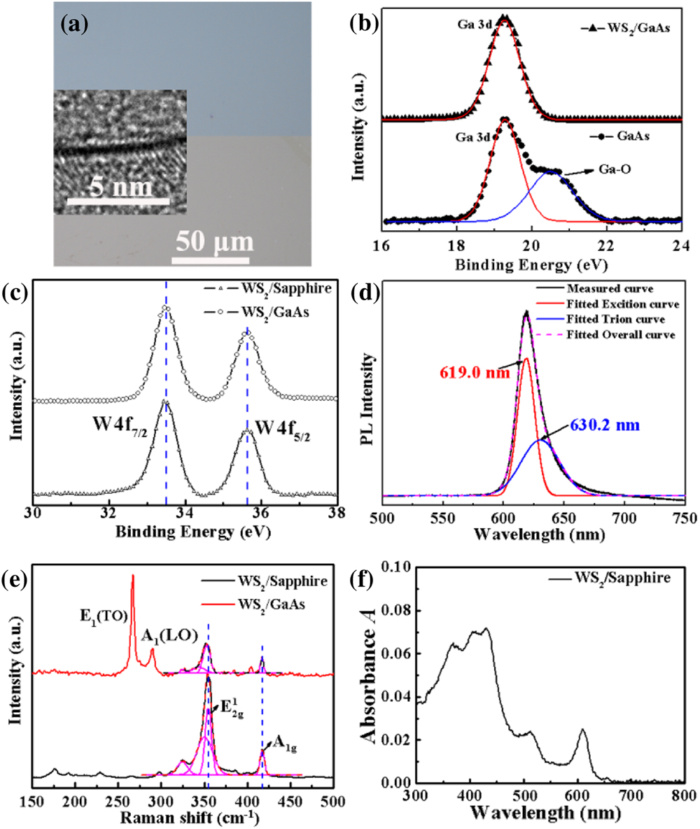
Figure 1.(a) Optical images of the sample (bottom) and sample (top). The inset image corresponds to the cross-sectional TEM result of . (b) The X ray photoelectron spectroscopy obtained from the uncleaned GaAs substrate and sample. (c) The W 4f spectrum of the and samples. (d) The room temperature photoluminescence spectrum of the monolayer grown on sapphire substrate, and the related fitted exciton and trion peaks. (e) Raman spectra of both monolayer and monolayer samples. (f) The absorbance spectrum of monolayer grown on sapphire substrate.
The schematic structure of the monolayer photodetector is shown in Fig. 2(a), and the insets are the related optical microscopy images of device arrays (left) and single device (right). Figure 2(b) displays the dark current and light current of both GaAs and photodetectors at different incident wavelength (365 nm, 460 nm, 660 nm, and 880 nm) as a function of voltage. For the photodetector, the ratio of ( represents light current and corresponds to dark current) under 365 nm and 880 nm illumination reaches and at the bias voltage of 1.0 V, respectively, which is much larger than the corresponding values (51 and 2.01) of the GaAs device, indicating a significant performance improvement by the introduction of monolayer and a wide response spectrum ranging from UV to near-infrared, which overcomes the limited bandgap of pure monolayer . The improvement of the ratio is not only attributed to the enhancement of light absorption but also the reduction of dark current. The depletion region formed at the interface owing to the type-II band alignment as shown in Fig. 2(c) contributes to the photo-generated carrier separation and the reduction of carrier recombination and nonrecombination. Notably, the current of the photodetector at zero bias profoundly increases from under a dark condition to at 365 nm, at 460 nm, at 660 nm, and at 880 nm, respectively, leading to high ratios. That is to say, the corresponding voltage of the lowest current observed from the light I–V curves is away from zero bias. Therefore, it means that the heterojunction device can function as a self-driven photodetector.

Figure 2.(a) Schematic structure of the photodetector, and the insets are the optical microscopy images of the device arrays (left) and single device (right). (b) Dark and light I–V curves of the GaAs photodetector (left) and photodetector (right) under different wavelength light illumination (365 nm, 460 nm, 660 nm, and 880 nm). (c) Schematic band diagrams at the interface of the heterojunction.
In order to further explore the performances of the fabricated devices, power-dependent optoelectronic measurements were taken for both photodetectors. Figures 3(a) and 3(b) show the I–V curves at 365 nm under different light power for the GaAs and devices, respectively. Then, the generated photocurrent () versus incident light power P at a bias voltage of 1.0 V is plotted in Figs. 3(c) and 3(d). The fitting results using the law labeled by the dashed lines in double logarithmic coordinates demonstrate a good superlinear relationship between photocurrent and incident light power. For the GaAs detector, is about 1.95 when the power is lower than 0.639 μW, indicating increases rapidly with the increase of the power in this range. However, it is reduced to 1.35 with the . A similar trend is also observed in the photodetector with about 1.63 and 1.00, and the turning point is 0.779 μW. The deduced value is usually less than 1.0 owing to the existence of trap states between the Fermi level and the conduction band edge in many reported results [32–35]. Herein, the origin of the large value () in both devices needs to be further investigated, whereas the transfer process inevitably introduces some trap states, which makes value of the photodetector smaller than those of the GaAs photodetector.
Figure 3.(a) and (b) show the dark and light I–V curves at 365 nm illumination under different incident light power of the GaAs and photodetectors, respectively. (c) and (d) are the photocurrent as a function of incident light power under 365 nm at a fixed voltage of 1.0 V for the GaAs and photodetectors, respectively. (e) and (f) are the corresponding photoresponsivity according to the photocurrent obtained above.
Photoresponsivity () as a figure of merit for the photodetector representing the photocurrent generated per unit of the incident power can be expressed by , where is the effective power illuminated on the active area of the device. The calculated versus laser power under 365 nm at the bias voltage of 1.0 V for both GaAs and devices is depicted in Figs. 3(e) and 3(f). Obviously, increases rapidly with incident power rising at the initial stage, and then the rising rate is slowed down, which is consistent with the phenomenon mentioned above. For the GaAs device, the minimum and maximum in the measured power range are 14.95 A/W and 30.04 A/W, respectively. The peak photoresponsivity of the photodetector is 65.58 A/W under incident light power of 0.938 μW, which is more than one time higher than the corresponding value of the compared GaAs device and the reported values of the photodetector (3.5 A/W) [15] and the nanosheet-based photodetector [36], but is much lower than that of the black phosphorus-based photodetector [37]. The and /RGO-based UV photodetectors have shown photoresponsivities of 80 μA/W and [38], respectively, which are much lower than our results. Meanwhile, it also far outweighs the reported value of the photovoltaic photodetector () [35] and the photodetector () [20], demonstrating the superiority of the combination between 2D- and 3D-GaAs semiconductors. At the near-infrared region 880 nm, the I–V curves, generated photocurrent, and photoresponsivity of the device under different light powers are exhibited in Figs. 4(a) and 4(b), respectively. The responsivity reaches as high as 28.5 A/W at 0.120 μW, which implies that the generated electron–hole pairs are not only from the transition between the valence band and conduction band of GaAs but also from the transition between the valence band of and conduction band of GaAs as illustrated in Fig. 2(c). Besides those, the performance of the detector at the visible region 460 nm is also shown in Figs. 4(c) and 4(d). The responsivity reaches about 7.5 A/W.
Figure 4.(a) Exhibits the dark and light I–V curves under 880 nm illumination with different incident light power of the photodetectors. (b) shows the corresponding photocurrent and photoresponsivity. (c) displays the dark and light I–V curves under 460 nm illumination with different incident light power of the photodetectors. (d) shows the corresponding photocurrent and photoresponsivity.
For photodetectors, detectivity is another important performance index, which stands for the ability of sensing weak signal. In order to have some in-depth insights into the detection limit and signal-to-noise ratio of the photodetectors, noise equivalent power (NEP) and normalized detectivity () are evaluated. NEP is estimated according to the following formula [39]: where is the elementary charge, is the dark current, and is the responsivity. A small NEP indicates a weak noise signal. Then, the normalized detectivity is defined by , where is the device active area ( here). Consequently, the power-dependent NEP and for GaAs and photodetectors characterized under 365 nm are plotted in Figs. 5(a) and 5(b), respectively. Apparently, lowest and highest are obtained in the device under 365 nm illumination at 1 V, which are an order of magnitude lower and higher than the corresponding values of the GaAs device, respectively. The performance of the photodetector in this work is better than the reported photodetector ( at 365 nm) [34], vertically aligned heterojunction photodetector () [40], and photodetector () [41].
Figure 5.(a) and (b) are the noise equivalent power (NEP) and normalized detectivity of both GaAs and photodetectors as a function of incident power, respectively.
Photo-switching characteristics have also been explored for the photodetector under a fixed voltage of at 365 nm in order to investigate the stability and response speed. The light is switched on/off alternately, and the time with/without illumination is set to 10 s. As shown in Fig. 6(a), the current rises to the on-state under illumination and then falls to the off-state under dark condition. The device exhibits stable switching behavior and repeatability without degradation of photo-response during the testing cycles. In addition, the corresponding rise time is normally confirmed as the time for the current increasing from 10% to 90% of the maximum photocurrent and the fall time is defined as the inverse (for the current decreasing from 90% to 10%). Then, the rise and fall times are determined to be 30 ms and 10 ms as shown in Fig. 6(b), respectively. This response speed is comparable to that of the reported photodetector (20 ms) [42], slower than that of the photodetector (rise time 16.2 μs) [35], but much faster than those of the photodetector (rise time 1.36 s) [43] and the reported photodetector (7.85 s) [44]. A consistent result is also obtained under 880 nm illumination as displayed in Figs. 6(c) and 6(d). However, the stability of the device needs to be further improved as shown in Fig. 6(a) that the current was reduced largely after three days, which is owing to the oxidation. The optimization of the material growth and transfer process or the device passivation technology is believed to be able to further improve the photocurrent switching performance and long-term stability of the device, which also provides us with a promising way to facilitate the application of in optoelectronics.
Figure 6.(a) and (c) are the photocurrent-time curves of photodetector at illuminated by 365 nm and 880 nm light, respectively. Meanwhile, the performance of the device under 365 nm after three days was also shown. (b) and (d) are the determined rise time (from 10% to 90% of maximum photocurrent) and fall time (from 90% to 10% of maximum photocurrent) of the detector under 365 nm and 880 nm light, respectively.
4. CONCLUSION
In conclusion, large-area monolayer was successfully synthesized using the CVD method and transferred onto GaAs substrate to fabricate heterojunction photodetectors. The detector exhibits an overall high performance, including high photoresponsivity of 65.58 A/W, low NEP of , high detectivity of , and a fast response speed of 30/10 ms, as well as self-driven photodetection ranging from the UV to near-infrared spectrum. This work reveals that the heterostructure has great potential in future optoelectronics, and also provides a low-cost, easy-to-process method for the preparation of 2D/3D heterojunction-based devices.
References
[1] A. K. Geim, K. S. Novoselov. The rise of graphene. Nat. Mater., 6, 183-191(2007).
[2] B. Radisavljevic, A. Radenovic, J. Brivio, V. Giacometti, A. Kis. Single-layer MoS2 transistors. Nat. Nanotechnol., 6, 147-150(2011).
[3] X. Gan, R.-J. Shiue, Y. Gao, I. Meric, T. F. Heinz, K. Shepard, J. Hone, S. Assefa, D. Englund. Chip-integrated ultrafast graphene photodetector with high responsivity. Nat. Photonics, 7, 883-887(2013).
[4] C. Wu, J. Z. Ou, F. He, J. Ding, W. Luo, M. Wu, H. Zhang. Three-dimensional MoS2/carbon sandwiched architecture for boosted lithium storage capability. Nano Energy, 65, 104061(2019).
[5] Q. H. Wang, M. S. Strano, K. Kalantar-Zadeh, A. Kis, J. N. Coleman. Electronics and optoelectronics of two-dimensional transition metal dichalcogenides. Nat. Nanotechnol., 7, 699-712(2012).
[6] G. Fiori, F. Bonaccorso, G. Iannaccone, T. Palacios, D. Neumaier, A. Seabaugh, S. K. Banerjee, L. Colombo. Electronics based on two-dimensional materials. Nat. Nanotechnol., 9, 768-779(2014).
[7] C. Cong, J. Shang, Y. Wang, T. Yu. Optical properties of 2D semiconductor WS2. Adv. Opt. Mater., 6, 1700767(2018).
[8] W. Wang, K. Li, Y. Wang, W. Jiang, X. Liu, H. Qi. Investigation of the band alignment at MoS2/PtSe2 heterojunctions. Appl. Phys. Lett., 114, 201601(2019).
[9] L. Han, M. Peng, Z. Wen, Y. Liu, Y. Zhang, Q. Zhu, H. Lei, S. Liu, L. Zheng, X. Sun, H. Li. Self-driven photodetection based on impedance matching effect between a triboelectric nanogenerator and a MoS2 nanosheets photodetector. Nano Energy, 59, 492-499(2019).
[10] Y.-C. Wu, W.-R. Liu. Few-layered MoSe2 ultrathin nanosheets as anode materials for lithium ion batteries. J. Alloys Compd., 813, 152074(2020).
[11] H.-J. Chuang, X. Tan, N. J. Ghimire, M. M. Perera, B. Chamlagain, M. M.-C. Cheng, J. Yan, D. Mandrus, D. Tománek, Z. Zhou. High mobility WSe2 p- and n-type field-effect transistors contacted by highly doped graphene for low-resistance contacts. Nano Lett., 14, 3594-3601(2014).
[12] J.-H. Lin, Y.-H. Tsao, M.-H. Wu, T.-M. Chou, Z.-H. Lin, J. M. Wu. Single- and few-layers MoS2 nanocomposite as piezo-catalyst in dark and self-powered active sensor. Nano Energy, 31, 575-581(2017).
[13] L. Yuan, L. Huang. Exciton dynamics and annihilation in WS2 2D semiconductors. Nanoscale, 7, 7402-7408(2015).
[14] J. D. Yao, Z. Q. Zheng, J. M. Shao, G. W. Yang. Stable, highly-responsive and broadband photodetection based on large-area multilayered WS2 films grown by pulsed-laser deposition. Nanoscale, 7, 14974-14981(2015).
[15] H. Tan, Y. Fan, Y. Zhou, Q. Chen, W. Xu, J. H. Warner. Ultrathin 2D photodetectors utilizing chemical vapor deposition grown WS2 with graphene electrodes. ACS Nano, 10, 7866-7873(2016).
[16] C. Lan, Z. Zhou, Z. Zhou, C. Li, L. Shu, L. Shen, D. Li, R. Dong, S. Yip, J. C. Ho. Wafer-scale synthesis of monolayer WS2 for high-performance flexible photodetectors by enhanced chemical vapor deposition. Nano Res., 11, 3371-3384(2018).
[17] Y. Liu, W. Huang, W. Chen, X. Wang, J. Guo, H. Tian, H. Zhang, Y. Wang, B. Yu, T.-L. Ren, J. Xu. Plasmon resonance enhanced WS2 photodetector with ultra-high sensitivity and stability. Appl. Surf. Sci., 481, 1127-1132(2019).
[18] D. Jariwala, T. J. Marks, M. C. Hersam. Mixed-dimensional van der Waals heterostructures. Nat. Mater., 16, 170-181(2017).
[19] P. Gehring, R. Urcuyo, D. L. Duong, M. Burghard, K. Kern. Thin-layer black phosphorus/GaAs heterojunction p-n diodes. Appl. Phys. Lett., 106, 233110(2015).
[20] Z. Xu, S. Lin, X. Li, S. Zhang, Z. Wu, W. Xu, Y. Lu, S. Xu. Monolayer MoS2/GaAs heterostructure self-driven photodetector with extremely high detectivity. Nano Energy, 23, 89-96(2016).
[21] H.-S. Kim, M. Patel, J. Kim, M. S. Jeong. Growth of wafer-scale standing layers of WS2 for self-biased high-speed UV-visible–NIR optoelectronic devices. ACS Appl. Mater. Interfaces, 10, 3964-3974(2018).
[22] Y. Lu, S. Feng, Z. Wu, Y. Gao, J. Yang, Y. Zhang, Z. Hao, J. Li, E. Li, H. Chen, S. Lin. Broadband surface plasmon resonance enhanced self-powered graphene/GaAs photodetector with ultrahigh detectivity. Nano Energy, 47, 140-149(2018).
[23] K. Li, W. Wang, J. Leng, B. Sun, D. Li, H. Yang, T. Jiang, Y. He. Carrier dynamics in monolayer WS2/GaAs heterostructures. Appl. Surf. Sci., 500, 144005(2020).
[24] T. Kato, T. Kaneko. Transport dynamics of neutral excitons and trions in monolayer WS2. ACS Nano, 10, 9687-9694(2016).
[25] K. F. Mak, K. He, C. Lee, G. H. Lee, J. Hone, T. F. Heinz, J. Shan. Tightly bound trions in monolayer MoS2. Nat. Mater., 12, 207-211(2012).
[26] K. Li, K.-W. Ang, Y. Lv, X. Liu. Effects of Al2O3 capping layers on the thermal properties of thin black phosphorus. Appl. Phys. Lett., 109, 261901(2016).
[27] K. Li, T. Wang, W. Wang, X. Gao. Lattice vibration properties of MoS2/PtSe2 heterostructures. J. Alloys Compd., 820, 153192(2020).
[28] X. Cong, M. Lin, P.-H. Tan. Lattice vibration and Raman scattering of two-dimensional van der Waals heterostructure. J. Semicond., 40, 091001(2019).
[29] W. Shi, M.-L. Lin, Q.-H. Tan, X.-F. Qiao, J. Zhang, P.-H. Tan. Raman and photoluminescence spectra of two-dimensional nanocrystallites of monolayer WS2 and WSe2. 2D Mater., 3, 025016(2016).
[30] C. Cong, J. Shang, X. Wu, B. Cao, N. Peimyoo, C. Qiu, L. Sun, T. Yu. Synthesis and optical properties of large-area single-crystalline 2D semiconductor WS2 monolayer from chemical vapor deposition. Adv. Opt. Mater., 2, 131-136(2014).
[31] A. M. Dadgar, D. Scullion, K. Kang, D. Esposito, E. H. Yang, I. P. Herman, M. A. Pimenta, E. J. G. Santos, A. N. Pasupathy. Strain engineering and Raman spectroscopy of monolayer transition metal dichalcogenides. Chem. Mater., 30, 5148-5155(2018).
[32] X. Yu, P. Yu, D. Wu, B. Singh, Q. Zeng, H. Lin, W. Zhou, J. Lin, K. Suenaga, Z. Liu, Q. J. Wang. Atomically thin noble metal dichalcogenide: a broadband mid-infrared semiconductor. Nat. Commun., 9, 1545(2018).
[33] L.-H. Zeng, M.-Z. Wang, H. Hu, B. Nie, Y.-Q. Yu, C.-Y. Wu, L. Wang, J.-G. Hu, C. Xie, F.-X. Liang, L.-B. Luo. Monolayer graphene/germanium Schottky junction as high-performance self-driven infrared light photodetector. ACS Appl. Mater. Interfaces, 5, 9362-9366(2013).
[34] L. Zeng, L. Tao, C. Tang, B. Zhou, H. Long, Y. Chai, S. P. Lau, Y. H. Tsang. High-responsivity UV-Vis photodetector based on transferable WS2 film deposited by magnetron sputtering. Sci. Rep., 6, 20343(2016).
[35] E. Wu, D. Wu, C. Jia, Y. Wang, H. Yuan, L. Zeng, T. Xu, Z. Shi, Y. Tian, X. Li. In situ fabrication of 2D WS2/Si type-II heterojunction for self-powered broadband photodetector with response up to mid-infrared. ACS Photon., 6, 565-572(2019).
[36] W. Huang, C. Xing, Y. Wang, Z. Li, L. Wu, D. Ma, X. Dai, Y. Xiang, J. Li, D. Fan, H. Zhang. Facile fabrication and characterization of two-dimensional bismuth(iii) sulfide nanosheets for high-performance photodetector applications under ambient conditions. Nanoscale, 10, 2404-2412(2018).
[37] Y. Liu, B. N. Shivananju, Y. Wang, Y. Zhang, W. Yu, S. Xiao, T. Sun, W. Ma, H. Mu, S. Lin, H. Zhang, Y. Lu, C.-W. Qiu, S. Li, Q. Bao. Highly efficient and air-stable infrared photodetector based on 2D layered graphene-black phosphorus heterostructure. ACS Appl. Mater. Interfaces, 9, 36137-36145(2017).
[38] N. T. Shelke, B. R. Karche. Hydrothermal synthesis of WS2/RGO sheet and their application in UV photodetector. J. Alloys Compd., 653, 298-303(2015).
[39] P. Hu, L. Wang, M. Yoon, J. Zhang, W. Feng, X. Wang, Z. Wen, J. C. Idrobo, Y. Miyamoto, D. B. Geohegan, K. Xiao. Highly responsive ultrathin GaS nanosheet photodetectors on rigid and flexible substrates. Nano Lett., 13, 1649-1654(2013).
[40] L.-H. Zeng, S.-H. Lin, Z.-J. Li, Z.-X. Zhang, T.-F. Zhang, C. Xie, C.-H. Mak, Y. Chai, S. P. Lau, L.-B. Luo, Y. H. Tsang. Fast, self-driven, air-stable, and broadband photodetector based on vertically aligned PtSe2/GaAs heterojunction. Adv. Funct. Mater., 28, 1705970(2018).
[41] J. Guo, S. Li, Y. Ke, Z. Lei, Y. Liu, L. Mao, T. Gong, T. Cheng, W. Huang, X. Zhang. Broadband photodetector based on vertically stage-liked MoS2/Si heterostructure with ultra-high sensitivity and fast response speed. Scripta Mater., 176, 1-6(2020).
[42] J. Yao, Z. Zheng, G. Yang. Layered-material WS2/topological insulator Bi2Te3 heterostructure photodetector with ultrahigh responsivity in the range from 370 to 1550 nm. J. Mater. Chem. C, 4, 7831-7840(2016).
[43] Y. Wu, Z. Li, K.-W. Ang, Y. Jia, Z. Shi, Z. Huang, W. Yu, X. Sun, X. Liu, D. Li. Monolithic integration of MoS2-based visible detectors and GaN-based UV detectors. Photon. Res., 7, 1127-1133(2019).
[44] C. Lan, C. Li, S. Wang, T. He, Z. Zhou, D. Wei, H. Guo, H. Yang, Y. Liu. Highly responsive and broadband photodetectors based on WS2–graphene van der Waals epitaxial heterostructures. J. Mater. Chem. C, 5, 1494-1500(2017).

