• Infrared and Laser Engineering
  • Vol. 51, Issue 4, 20210942 (2022)
Yu Zhu1, Shihan Yan2、3、*, Ziyi Zang2、4, Shengxing Song1, Jie Wang2、4, Zhanqiang Ru1, Hongliang Cui2、4, and Helun Song1、*
Author Affiliations
  • 1Suzhou Institute of Nano-Tech and Nano-Bionics, Chinese Academy of Sciences, Suzhou 215123, China
  • 2Chongqing Institute of Green and Intelligent Technology, Chinese Academy of Sciences, Chongqing 400714, China
  • 3Chongqing School, University of Chinese Academy of Sciences, Chongqing 400714, China
  • 4College of Instrumentation and Electrical Engineering, Jilin University, Changchun 130061, China
  • show less
    DOI: 10.3788/IRLA20210942 Cite this Article
    Yu Zhu, Shihan Yan, Ziyi Zang, Shengxing Song, Jie Wang, Zhanqiang Ru, Hongliang Cui, Helun Song. Application of terahertz mapping in high throughput measurement of the electrical conductance of Cu alloy thin films (Invited)[J]. Infrared and Laser Engineering, 2022, 51(4): 20210942 Copy Citation Text show less
    Illustration of the high throughput materials chip fabrication method with electron beam deposition. (a) 12×12 mask of 3 patterns; (b) Illustration of the in site discrete mode process; (c) System setup for e-beam source, mask and sample stage; (d) Illustration of the ternary continuous gradient process; (e) Illustration of heat treatment process
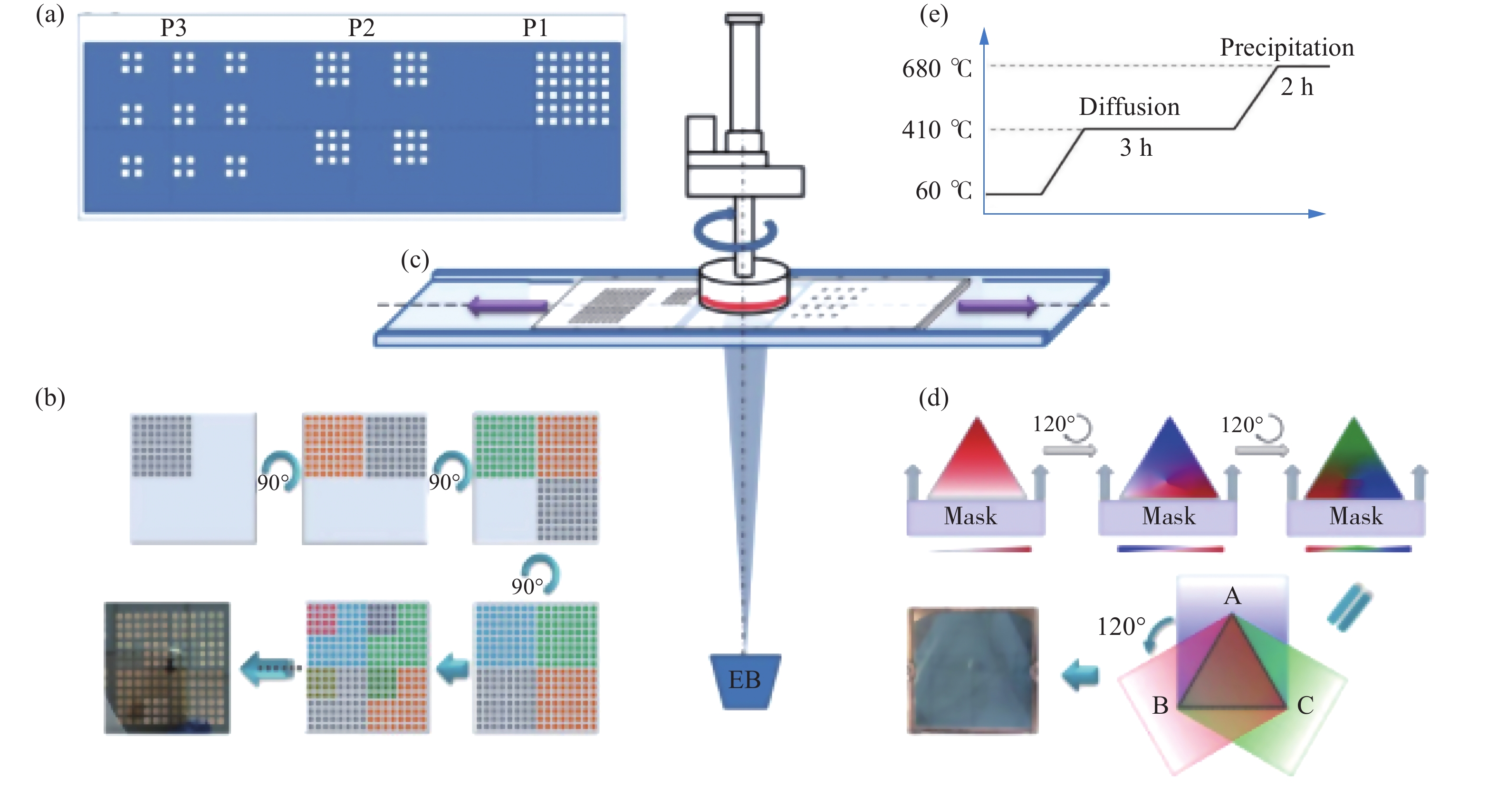
    Fig. 1. Illustration of the high throughput materials chip fabrication method with electron beam deposition. (a) 12×12 mask of 3 patterns; (b) Illustration of the in site discrete mode process; (c) System setup for e-beam source, mask and sample stage; (d) Illustration of the ternary continuous gradient process; (e) Illustration of heat treatment process
    (a) Illustration of the THz mapping detection system in transmission mode; (b) THz time-domain spectra of the periodic temporal signals from multiple internal reflections; (c) Experimental setup of the THz emitter, the sample stage and the photoconductive detector
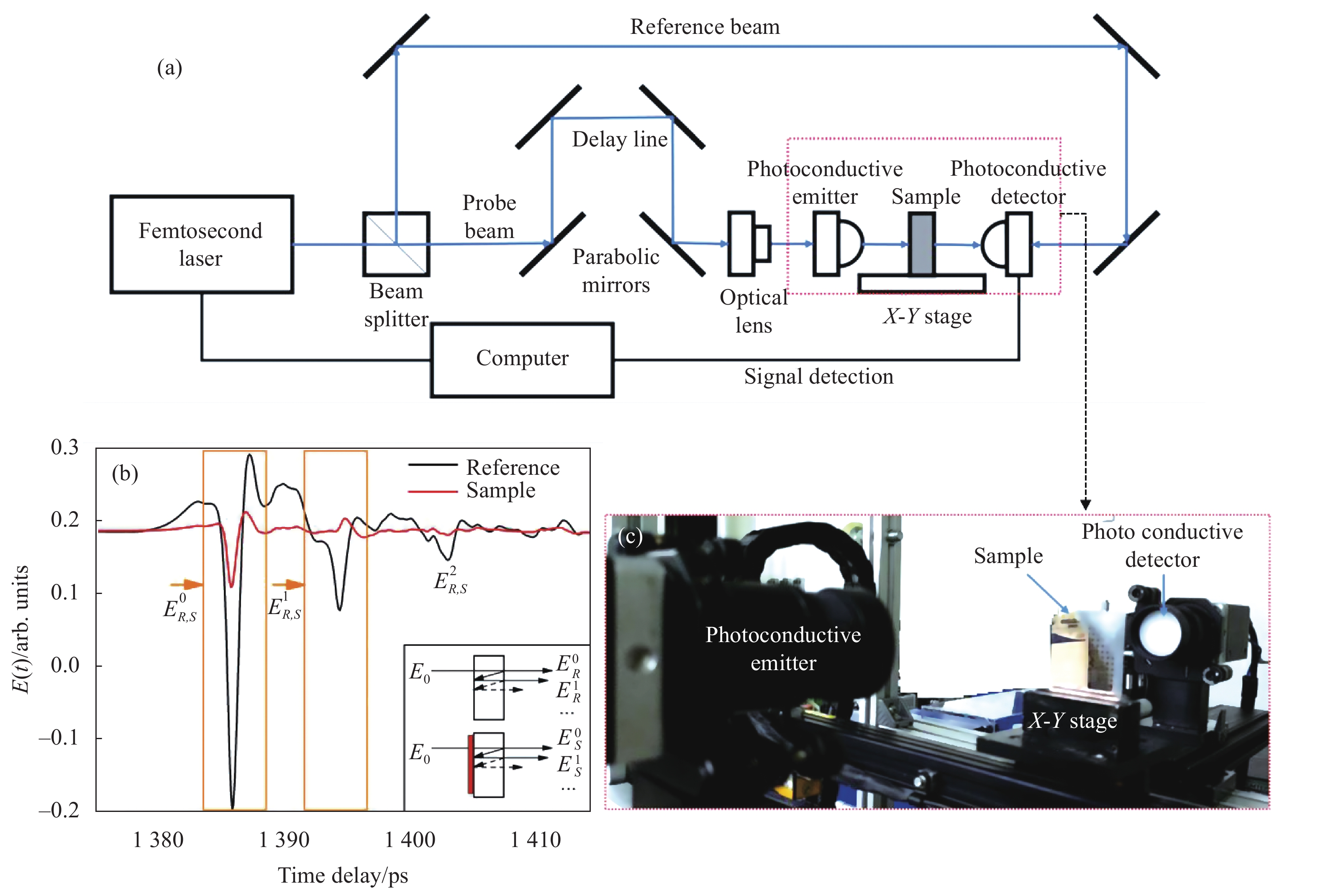
    Fig. 2. (a) Illustration of the THz mapping detection system in transmission mode; (b) THz time-domain spectra of the periodic temporal signals from multiple internal reflections; (c) Experimental setup of the THz emitter, the sample stage and the photoconductive detector
    (a)-(c) Optical images of the samples; (d)-(f) THz conductance imaging of the corresponding samples; (g) Comparison of metal film conductance obtained by different test methods
    Fig. 3. (a)-(c) Optical images of the samples; (d)-(f) THz conductance imaging of the corresponding samples; (g) Comparison of metal film conductance obtained by different test methods
    (a) Cu thin film sample photo on high resistivity Si substrate; (b) THz conductance mapping image; (c) THz conductance variations of the sample spots; (d) Anisotropic variations along the horizontal direction of Fig.(a) and (b); (e) Anisotropic variations along the vertical direction of Fig.(a) and (b)
    Fig. 4. (a) Cu thin film sample photo on high resistivity Si substrate; (b) THz conductance mapping image; (c) THz conductance variations of the sample spots; (d) Anisotropic variations along the horizontal direction of Fig.(a) and (b); (e) Anisotropic variations along the vertical direction of Fig.(a) and (b)
    Cu-Al2O3/Ag/Mg alloy thin film sample fabricated with the continuous gradient mode. (a) Optical image of the sample; (b) THz mapping imaging, scale bar=4 mm; (c) Comparison between the conductance trend of the 15 points marked in Fig.(b) obtained from THz and 4-point probe respectively
    Fig. 5. Cu-Al2O3/Ag/Mg alloy thin film sample fabricated with the continuous gradient mode. (a) Optical image of the sample; (b) THz mapping imaging, scale bar=4 mm; (c) Comparison between the conductance trend of the 15 points marked in Fig.(b) obtained from THz and 4-point probe respectively
    Cu-Al2O3/Ag/Mg alloy thin film sample fabricated with the in site discrete mode. (a) Optical image of the sample; (b) THz mapping imaging; (c) Simulated combination of the thickness and positions of the constituents; (d) Index table of the sample spots; (e) Deposition parameters of multi-layer film
    Fig. 6. Cu-Al2O3/Ag/Mg alloy thin film sample fabricated with the in site discrete mode. (a) Optical image of the sample; (b) THz mapping imaging; (c) Simulated combination of the thickness and positions of the constituents; (d) Index table of the sample spots; (e) Deposition parameters of multi-layer film
    SEM images of the 12×12 Cu-Al2O3/Ag/Mg Cu alloy thin film samples array, scale bar=100 μm
    Fig. 7. SEM images of the 12×12 Cu-Al2O3/Ag/Mg Cu alloy thin film samples array, scale bar=100 μm
    (a) Relationship between the THz mapping conductance and that of the weight percentage of the samples constituents from column 164-214; (b) SEM microstructure morphology of representative sample spots with different conductance
    Fig. 8. (a) Relationship between the THz mapping conductance and that of the weight percentage of the samples constituents from column 164-214; (b) SEM microstructure morphology of representative sample spots with different conductance
    Sample constituentsConductance/SRD (THz-4PP)/4PP
    THz4PP
    ATi 56 nm0.02140.02092.39%
    BTi 56 nm+Zr 30 nm0.01920.021510.7%
    CTi 56 nm+Zr 30 nm+Al 24 nm0.1460.17817.8%
    Table 1. Conductance value of metal films
    Layer indexMaterialsThickness/nm
    1Ti5
    2Cu80
    3Ag0→ 12.7
    4Cu10
    5Al2O30→ 12.7
    6Cu10
    7Mg0→ 25.4
    8Cu10
    Table 2. Constituents of the sample fabricated using the continuous gradient mode
    12345
    4PP1.141.151.320.980.97
    THz0.760.860.910.590.66
    RD−0.33%−0.25%−0.31%−0.40%−0.32%
    678910
    4PP1.542.152.891.010.88
    THz1.061.472.240.770.64
    RD−0.31%−0.32%−0.22%−0.24%−0.27%
    1112131415
    4PP0.650.720.810.90.84
    THz0.510.530.590.70.6
    RD−0.22%−0.26%−0.27%−0.22%−0.29%
    Table 3. Conductance of the selected 15 points along the thickness gradients of Ag, Mg and Al2O3 using 4-point probe and THz methods respectively
    0.175 60.101 80.175 60.179 80.180 10.178 10.159 10.173 40.151 00.127 00.172 10.195 6
    0.082 50.060 60.188 00.203 70.202 10.188 00.172 00.193 30.183 80.151 90.195 70.211 3
    0.192 10.180 70.194 90.210 00.203 30.204 80.153 70.167 70.190 40.171 90.176 10.209 0
    0.212 50.207 90.223 00.271 70.216 50.215 50.173 40.197 70.214 80.218 40.243 90.248 5
    0.078 90.076 90.185 20.223 40.223 90.231 50.178 10.194 40.215 40.222 90.256 10.220 7
    0.079 20.077 70.184 00.210 70.225 70.218 70.172 20.200 90.240 60.222 10.234 20.223 9
    0.198 50.203 50.168 50.216 80.231 40.223 00.190 20.194 40.276 30.264 50.262 10.266 8
    0.188 60.186 70.154 30.206 50.191 70.197 80.189 10.201 30.238 90.238 70.250 10.268 3
    0.033 80.040 60.101 50.181 30.072 50.077 60.177 30.193 60.165 30.162 80.251 20.268 7
    0.030 50.042 40.111 40.175 80.083 20.097 40.179 60.189 60.177 30.148 50.237 70.246 1
    0.161 60.159 50.141 70.213 60.179 10.183 20.165 40.179 80.244 80.222 80.248 90.258 8
    0.173 60.168 90.144 90.224 30.181 80.187 60.155 90.175 10.226 50.216 70.242 60.250 5
    Table 4. THz conductance value of the in site discrete 12×12 Cu-Al2O3/Ag/Mg alloy sample library
    Sample indexTHz conductance/SO/wt%
    2630.27635.05
    2640.26456.76
    1430.19047.36
    2330.17738.03
    2340.148516.24
    3330.111411.46
    3360.097425.1
    Table 5. Comparison of THz conductance and the weight percentage of oxygen of representative sample spots
    Sample index THz conductance/S O/wt%Al/wt%Ag/wt%Mg/wt%
    1640.1278.737.795.835.58
    1540.151 94.948.194.996.51
    1440.171 97.195.755.382.13
    1340.218 46.277.4710.153.79
    1240.222 96.654.6510.385.11
    1140.222 18.056.939.764.27
    2640.264 56.766.396.213.65
    2540.238 77.875.985.463.56
    2440.162 812.919.67.744.26
    2340.148 516.2411.8510.774.61
    2240.222 85.886.5511.124.23
    2140.216 76.76.0310.252.8
    Table 6. THz conductance and weight percentages of the constituents of sample spots in column #164-#214
    Measurement of electrical conductance/conductivityTerahertz mappingFour point probe
    Detection modeContactlessContact with sample
    Applications[12-14]Suitable for large samples or micro sampling(<2 mm), uniform or non-uniformSample area ≥10 mm2, uniform
    Conductivity mapping of graphene and carbon nanotubes, measurements of semiconductors, metallic thin films, superconductors, and metal oxides, etc. High throughput mapping of Conductance of Cu alloy thin films in the present study Bulk or thin plates of conducting metals or semiconductors
    Efficiency of measurement High throughput 144 samples/compositions per chip/batch in the present study Low throughput
    Information extractedDiscrete value and mapping of conductivity, complex conductivity, charge/carrier mobility; electron scattering, etc.Discrete value of DC conductivity
    Detection resolutionThree dimensionalTwo dimensional
    Overall resultsComparison of multiple samples with various compositions prepared in one batch under same conditions in the present studyOne singular sample prepared each time
    Table 7. Advantages of THz scanning method vs. 4-point probe
    Yu Zhu, Shihan Yan, Ziyi Zang, Shengxing Song, Jie Wang, Zhanqiang Ru, Hongliang Cui, Helun Song. Application of terahertz mapping in high throughput measurement of the electrical conductance of Cu alloy thin films (Invited)[J]. Infrared and Laser Engineering, 2022, 51(4): 20210942
    Download Citation