
Ran Hao, Gaoyang Ye, Jianyao Jiao, Erping Li, "Increasing the bandwidth of slow light in fishbone-like grating waveguides," Photonics Res. 7, 240 (2019)
- Photonics Research
- Vol. 7, Issue 2, 240 (2019)
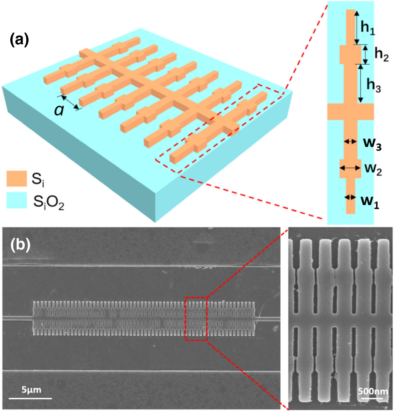
Fig. 1. (a) Schematic picture of the proposed FBGW; (b) SEM picture of the top view of the FBGW. Insets show the amplified picture of the red rectangle area.
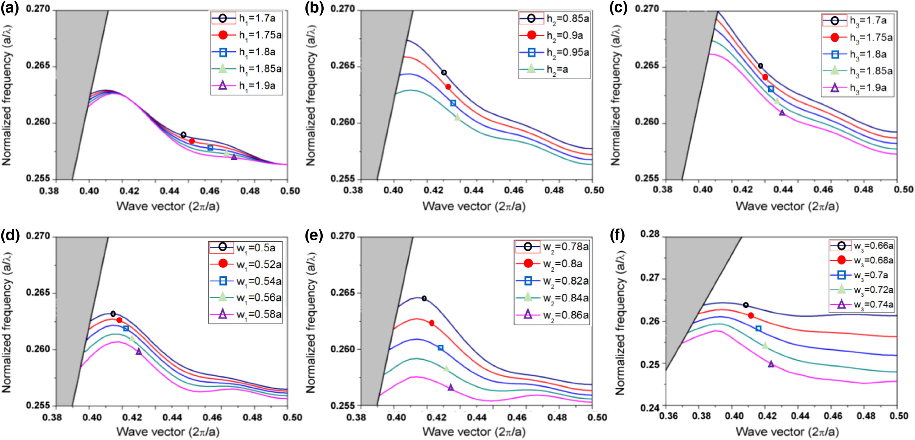
Fig. 2. Band variation with (a) h 1 h 2 = a h 3 = 1.85 a w 1 = 0.52 a w 2 = 0.8 a w 3 = 0.68 a h 2 h 1 = 1.7 a h 3 = 1.85 a w 1 = 0.52 a w 2 = 0.8 a w 3 = 0.68 a h 3 h 1 = 1.7 a h 2 = 0.85 a w 1 = 0.52 a w 2 = 0.8 a w 3 = 0.68 a w 1 h 1 = 1.85 a h 2 = a h 3 = 1.85 a w 2 = 0.8 a w 3 = 0.68 a w 2 h 1 = 1.85 a h 2 = a h 3 = 1.85 a w 1 = 0.52 a w 3 = 0.68 a w 3 h 1 = 1.85 a h 2 = a h 3 = 1.85 a w 1 = 0.52 a w 2 = 0.8 a
Fig. 3. (a) Band diagram for the 1D fishbone grating waveguide; the inset pictures are the electric fields of A and B, respectively; (b) group index n g h 1 = 1.7 a h 2 = 0.85 a h 3 = 1.75 a w 1 = 0.52 a w 2 = 0.8 a w 3 = 0.68 a h 1 = 1.85 a h 2 = a h 3 = 1.85 a w 1 = 0.52 a w 2 = 0.8 a w 3 = 0.68 a h 1 = 1.9 a h 2 = a h 3 = 1.85 a w 1 = 0.52 a w 2 = 0.8 a w 3 = 0.68 a
Fig. 4. (a) Temporal pulse detected at the input and the output; (b) simulated transmission of different periods, the inset is the SEM image of the step taper.
Fig. 5. (a) Schematic of the experimental setup. Inset pictures are SEM images of the grating coupler. In addition, we utilize a tunable laser (TL) source, a polarization controller (PC), a data analyzer (DA), and an optical spectrum analyzer (OSA). (b) Measured transmission and group index as functions of wavelength; (c) group index (from both simulation and experiment) as a function of wavelength.


Set citation alerts for the article
Please enter your email address

© Copyright 2018-2021 | Chinese Laser Press. All Rights Reserved 沪ICP备15018463号-20