• Journal of Infrared and Millimeter Waves
  • Vol. 43, Issue 1, 15 (2024)
Miao He1、2, Yi Zhou1、2、3、*, Xiang-Xiao Ying2, Zhao-Min Liang2, Min Huang2, Zhi-Fang Wang1、2, Yi-Hong Zhu2, Ke-Cai Liao2, Nan Wang2, and Jian-Xin Chen2、3
Author Affiliations
  • 1University of Shanghai for Science and Technology,Shanghai 200433
  • 2Shanghai Institute of Technical Physics,Shanghai 200083
  • 3School of Physics and Optoelectronic Engineering,Hangzhou Institute for Advanced Study,University of Chinese Academy of Sciences,Hangzhou 310024
  • show less
    DOI: 10.11972/j.issn.1001-9014.2024.01.003 Cite this Article
    Miao He, Yi Zhou, Xiang-Xiao Ying, Zhao-Min Liang, Min Huang, Zhi-Fang Wang, Yi-Hong Zhu, Ke-Cai Liao, Nan Wang, Jian-Xin Chen. Si Ion Implantation Study of InAs/GaSb Type II superlattice Materials[J]. Journal of Infrared and Millimeter Waves, 2024, 43(1): 15 Copy Citation Text show less

    Abstract

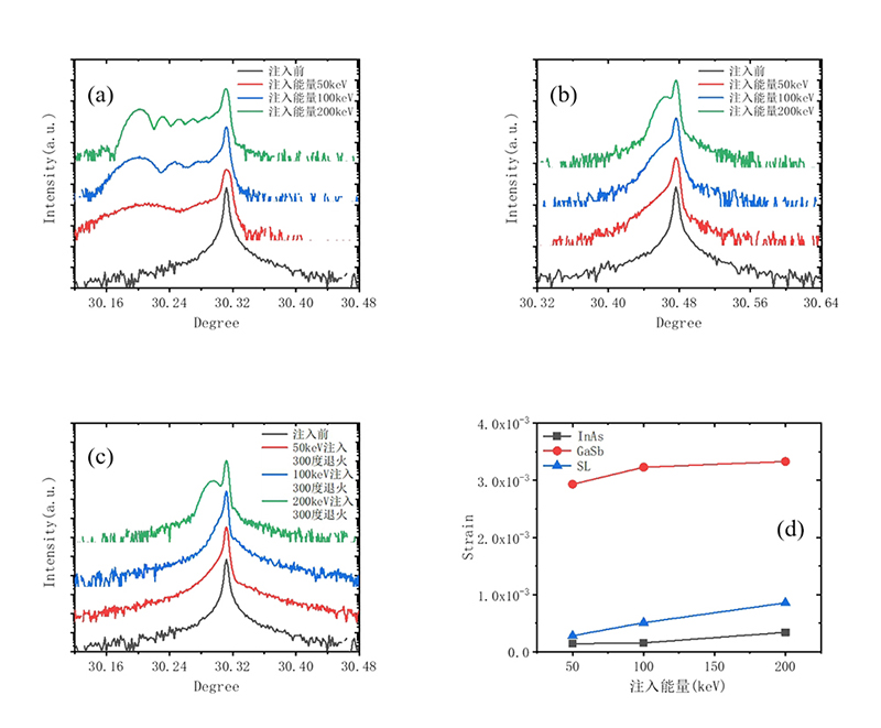
    Class II superlattice infrared detectors generally detect infrared radiation through mesa junction, while transverse PN junction is realized through ion implantation. On the one hand, the material epitaxy process is simple, and at the same time, the advantages of superlattice material that the transverse diffusion length is far higher than the longitudinal can be used to improve the transport of photogenerated current carriers, and it is easy to make high-density planar arrays. In this paper, the effects of Si ion implantation with different energies and annealing on the properties of InAs/GaSb type II superlattice materials were studied by using a variety of material characterization techniques. Through Si ion implantation, the epitaxial material changes from P type to N type, and the vertical tensile strain is generated in the superlattice material. The lattice constant becomes larger, and the mismatch increases with the increase of implantation energy. The mismatch before implantation is -0.012%. When the implantation energy reaches 200 keV, the mismatch reaches 0.072%, and the superlattice partially relaxes, with the relaxation degree of 14%. After annealing at 300 ° C for 60 s, the superlattice returns to the fully strained state, and the lattice constant becomes smaller, This tensile strain is caused by the diffusion of Ga-In caused by annealing and lattice shrinkage caused by Si substitution.
    Miao He, Yi Zhou, Xiang-Xiao Ying, Zhao-Min Liang, Min Huang, Zhi-Fang Wang, Yi-Hong Zhu, Ke-Cai Liao, Nan Wang, Jian-Xin Chen. Si Ion Implantation Study of InAs/GaSb Type II superlattice Materials[J]. Journal of Infrared and Millimeter Waves, 2024, 43(1): 15
    Download Citation