
Zongjie Bao, Chengwei Wang, Yang Zhang, Quan-Zhong Zhao, "Modification of wettability of stainless steel by picosecond laser surface microstructuring," Photonics Res. 3, 180 (2015)
- Photonics Research
- Vol. 3, Issue 4, 180 (2015)
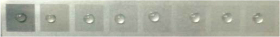
Fig. 1. Image of the treated areas under different parameters. From the first to the eighth areas, scanning speeds and intervals are 400 μm/s and 20 μm, 1000 μm/s and 40 μm, 2000 μm/s and 60 μm, 3000 μm/s and 80 μm, 4000 μm/s and 100 μm, 5000 μm/s and 120 μm, 6000 μm/s and 140 μm, 7000 μm/s and 160 μm, respectively.
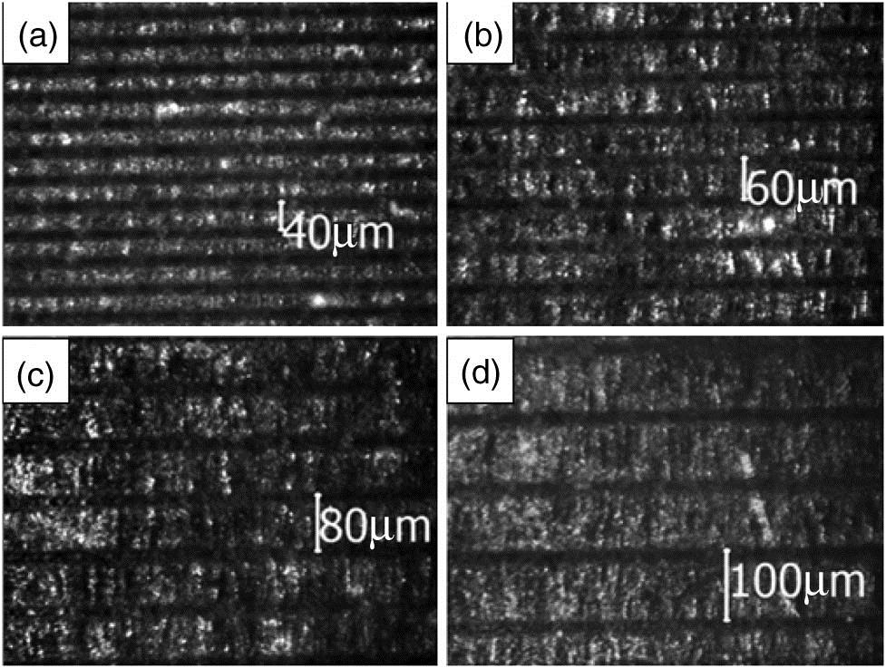
Fig. 2. OM images of the treated AISI 304 stainless steels under different parameters: (a) 1000 μm/s scanning speed and 40 μm scanning interval, (b) 2000 μm/s scanning speed and 60 μm scanning interval, (c) 3000 μm/s scanning speed and 80 μm scanning interval, and (d) 4000 μm/s scanning speed and 100 μm scanning interval.
Fig. 3. (a) SEM image of the treated AISI 304 stainless steel under 2000 μm/s scanning speed and 60 μm scanning interval with four periods of microstructures, (b) SEM image of the treated AISI 304 stainless steel with two periods of microstructures, (c) SEM image of the cavities and mastoids fabricated on the surface, and (d) SEM image of the low spatial frequency picosecond laser-induced periodic surface structures.
Fig. 4. Alteration of static contact angle under different scanning intervals and different scanning speeds when processing AISI 304 stainless steel.
Fig. 5. Alteration of static contact angle under different scanning intervals and different scanning speeds when processing AISI 316 stainless steel, respectively.


Set citation alerts for the article
Please enter your email address

© Copyright 2018-2021 | Chinese Laser Press. All Rights Reserved 沪ICP备15018463号-20