• Acta Physica Sinica
  • Vol. 69, Issue 17, 177103-1 (2020)
Yi-Xun Jiang1, Ming Qiao1、*, Wen-Ming Gao2, Xiao-Dong He2, Jun-Bo Feng1, Sen Zhang2, and Bo Zhang1
Author Affiliations
  • 1State Key Laboratory of Electronic Thin Film and Integrated Devices, University of Electronic Science and Technology of China, Chendu 610054, China
  • 2CSMC Technologies Corporation, Wuxi 214028, China
  • show less
    DOI: 10.7498/aps.69.20200359 Cite this Article
    Yi-Xun Jiang, Ming Qiao, Wen-Ming Gao, Xiao-Dong He, Jun-Bo Feng, Sen Zhang, Bo Zhang. A compact model of shield-gate trench MOSFET based on BSIM4[J]. Acta Physica Sinica, 2020, 69(17): 177103-1 Copy Citation Text show less
    (a) Distribution of equivalent resistance of SGT MOS; (b) equivalent DC circuit of SGT MOS.
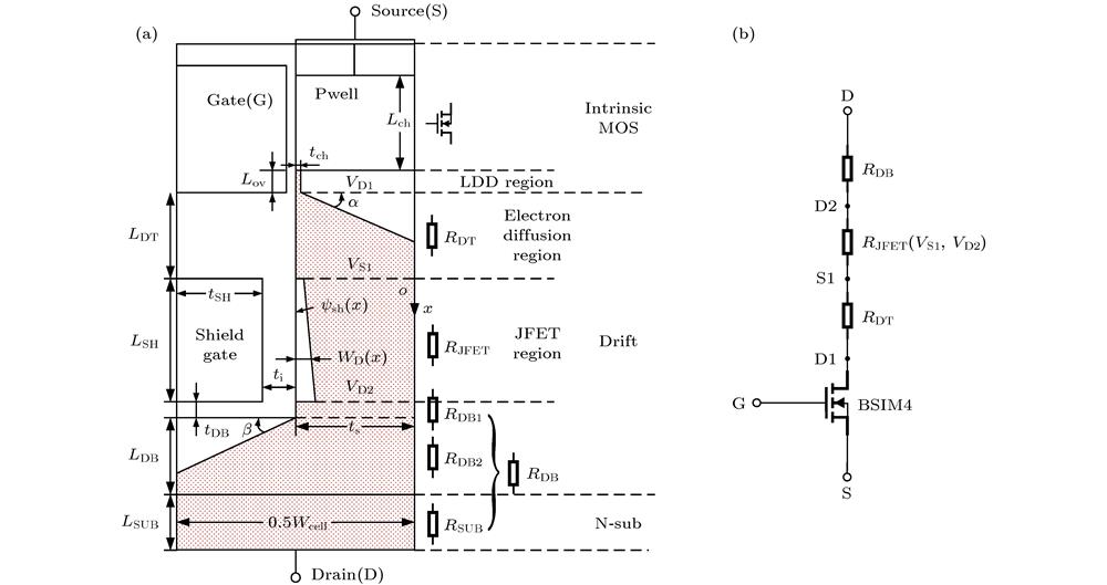
    Fig. 1. (a) Distribution of equivalent resistance of SGT MOS; (b) equivalent DC circuit of SGT MOS.
    (a) Distribution of capacitance and charge of SGT MOS; (b) equivalent capacitance circuit of SGT MOS.
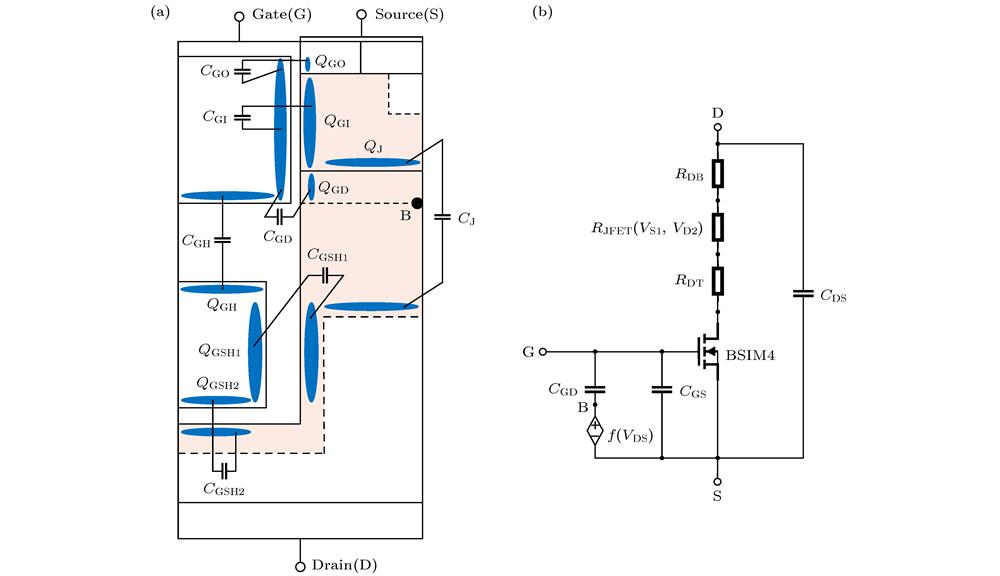
    Fig. 2. (a) Distribution of capacitance and charge of SGT MOS; (b) equivalent capacitance circuit of SGT MOS.
    Schematic diagrams of structure before equivalence (a) and after equivalence (b).
    Fig. 3. Schematic diagrams of structure before equivalence (a) and after equivalence (b).
    The curves of (a) transfer characteristic, (b) transconductance Gm, (c) output characteristic and (d) output conductance GDS at 25 ℃.
    Fig. 4. The curves of (a) transfer characteristic, (b) transconductance Gm, (c) output characteristic and (d) output conductance GDS at 25 ℃.
    The curves of (a) transfer characteristic, (b) transconductance Gm, (c) output characteristic and (d) output conductance GDS at 150 ℃.
    Fig. 5. The curves of (a) transfer characteristic, (b) transconductance Gm, (c) output characteristic and (d) output conductance GDS at 150 ℃.
    Capacitance curves on bias voltage: (a) Curve of CGD on VDS; (b) curve of CGS on VDS; (c) curve of CDS on VDS; (d) curves of Ciss, Coss and Crss on VDS.
    Fig. 6. Capacitance curves on bias voltage: (a) Curve of CGD on VDS; (b) curve of CGS on VDS; (c) curve of CDS on VDS; (d) curves of Ciss, Coss and Crss on VDS.
    Verification of switching characteristic: (a) Switching characteristic test circuit; (b) switching characteristic curve at Ion = 10 A
    Fig. 7. Verification of switching characteristic: (a) Switching characteristic test circuit; (b) switching characteristic curve at Ion = 10 A
    参数名含义大小/μm
    tox栅氧厚度0.07
    ti屏蔽栅与漂移区间氧化层厚度0.18
    ts槽右侧漂移区宽度0.30
    tDB屏蔽栅底部与漂移区的距离0.07
    Lch沟道长度0.53
    Lov栅与漂移区重叠部分的长度0.10
    LDT栅与屏蔽栅间距0.52
    LSH屏蔽栅长度0.87
    Wcell元胞宽度1.20
    Table 1. The size of SGT MOS.
    Yi-Xun Jiang, Ming Qiao, Wen-Ming Gao, Xiao-Dong He, Jun-Bo Feng, Sen Zhang, Bo Zhang. A compact model of shield-gate trench MOSFET based on BSIM4[J]. Acta Physica Sinica, 2020, 69(17): 177103-1
    Download Citation