• Photonics Research
  • Vol. 9, Issue 6, 1117 (2021)
Frank Mehnke1、3、*, Christian Kuhn1, Martin Guttmann1, Luca Sulmoni1, Verena Montag1, Johannes Glaab2, Tim Wernicke1, and Michael Kneissl1、2
Author Affiliations
  • 1Institute of Solid State Physics, Technische Universität Berlin, 10623 Berlin, Germany
  • 2Ferdinand-Braun-Institut, Leibniz-Institut für Höchstfrequenztechnik, 12489 Berlin, Germany
  • 3Current address: School of Electrical and Computer Engineering, Georgia Institute of Technology, Atlanta, Georgia 30332, USA
  • show less
    DOI: 10.1364/PRJ.414315 Cite this Article Set citation alerts
    Frank Mehnke, Christian Kuhn, Martin Guttmann, Luca Sulmoni, Verena Montag, Johannes Glaab, Tim Wernicke, Michael Kneissl. Electrical and optical characteristics of highly transparent MOVPE-grown AlGaN-based tunnel heterojunction LEDs emitting at 232 nm[J]. Photonics Research, 2021, 9(6): 1117 Copy Citation Text show less
    HR-XRD RSM near the AlN (10.5) reflex of a TJ LED heterostructure. Peaks corresponding to the individual layers are labeled in the graphic.
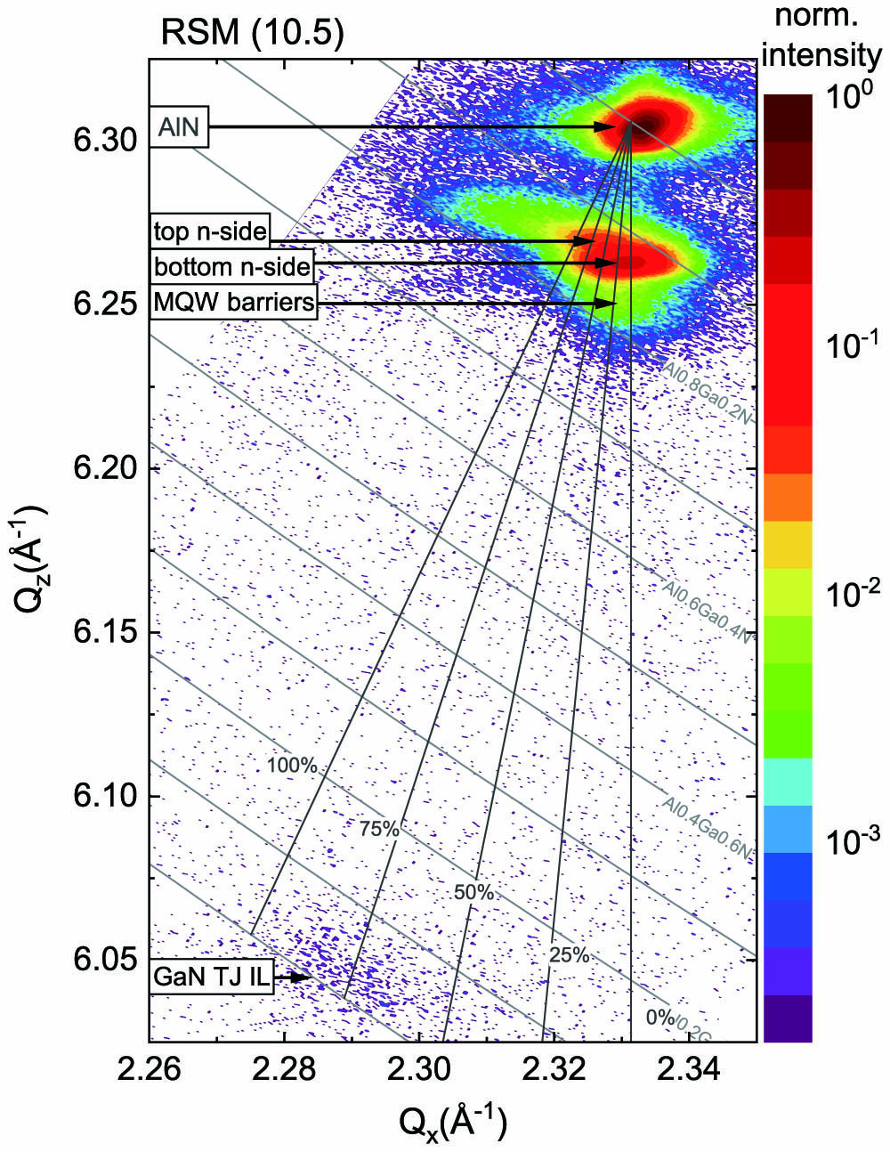
    Fig. 1. HR-XRD RSM near the AlN (10.5) reflex of a TJ LED heterostructure. Peaks corresponding to the individual layers are labeled in the graphic.
    Differential resistivity as a function of the bandgap and Al mole fraction at the TJ interface as reported for III-nitride LEDs [15,18,26–35" target="_self" style="display: inline;">–35]. Open and full symbols represent MBE- and MOVPE-grown heterostructures, respectively.
    Fig. 2. Differential resistivity as a function of the bandgap and Al mole fraction at the TJ interface as reported for III-nitride LEDs [15,18,2635" target="_self" style="display: inline;">35]. Open and full symbols represent MBE- and MOVPE-grown heterostructures, respectively.
    Spectral power density versus emission wavelength plot for a 232 nm TJ LED (A=0.15 mm2) measured through the bottom substrate (solid line) and top surface (dotted line) at a dc current of 5 mA. The inset shows a UV-sensitive microscopy image of a square-shaped frame top n-contact (A=0.04 mm2) measured at 5 mA through the top surface.
    Fig. 3. Spectral power density versus emission wavelength plot for a 232 nm TJ LED (A=0.15  mm2) measured through the bottom substrate (solid line) and top surface (dotted line) at a dc current of 5 mA. The inset shows a UV-sensitive microscopy image of a square-shaped frame top n-contact (A=0.04  mm2) measured at 5 mA through the top surface.
    (a) LIV characteristics and EQE of a TJ LED measured through the bottom substrate (solid lines) and the top surface (dashed lines). Far-field emission pattern measured on-wafer of (b) the bottom and (c) the top hemispheres at a constant current of 5 mA. The black dashed lines in (b) and (c) indicate the detectable emission by the bottom and top EL setup as shown in (a).
    Fig. 4. (a) LIV characteristics and EQE of a TJ LED measured through the bottom substrate (solid lines) and the top surface (dashed lines). Far-field emission pattern measured on-wafer of (b) the bottom and (c) the top hemispheres at a constant current of 5 mA. The black dashed lines in (b) and (c) indicate the detectable emission by the bottom and top EL setup as shown in (a).
    (a) LIV characteristics and EQE of a TJ LED with an aluminum reflector on the top surface as measured through the bottom substrate. (b) Far-field emission pattern measured on-wafer of the bottom hemisphere at a constant current of 5 mA. The black dashed line indicates the detectable emission by the bottom EL setup as shown in (a).
    Fig. 5. (a) LIV characteristics and EQE of a TJ LED with an aluminum reflector on the top surface as measured through the bottom substrate. (b) Far-field emission pattern measured on-wafer of the bottom hemisphere at a constant current of 5 mA. The black dashed line indicates the detectable emission by the bottom EL setup as shown in (a).
    Schematic TJ LED heterostructure and simulated LEE of (left) a TJ LED without aluminum reflector, (center) a TJ LED with large-area aluminum reflector, and (right) a TJ LED with large-area V/Al n-contact.
    Fig. 6. Schematic TJ LED heterostructure and simulated LEE of (left) a TJ LED without aluminum reflector, (center) a TJ LED with large-area aluminum reflector, and (right) a TJ LED with large-area V/Al n-contact.
    On-wafer measured bottom LIV characteristics in cw (solid lines) and pulsed mode operation (bullets) of a tunnel heterojunction LED (A=0.15 mm2) with aluminum reflector.
    Fig. 7. On-wafer measured bottom LIV characteristics in cw (solid lines) and pulsed mode operation (bullets) of a tunnel heterojunction LED (A=0.15  mm2) with aluminum reflector.
    Frank Mehnke, Christian Kuhn, Martin Guttmann, Luca Sulmoni, Verena Montag, Johannes Glaab, Tim Wernicke, Michael Kneissl. Electrical and optical characteristics of highly transparent MOVPE-grown AlGaN-based tunnel heterojunction LEDs emitting at 232 nm[J]. Photonics Research, 2021, 9(6): 1117
    Download Citation