
Frank Mehnke, Christian Kuhn, Martin Guttmann, Luca Sulmoni, Verena Montag, Johannes Glaab, Tim Wernicke, Michael Kneissl. Electrical and optical characteristics of highly transparent MOVPE-grown AlGaN-based tunnel heterojunction LEDs emitting at 232 nm[J]. Photonics Research, 2021, 9(6): 1117
- Photonics Research
- Vol. 9, Issue 6, 1117 (2021)
Abstract
1. INTRODUCTION
Light-emitting diodes (LEDs) emitting in the ultraviolet (UV) spectral region below 240 nm are of great interest, as they enable applications such as gas sensing of, e.g., nitrogen oxide (NO) and ammonia () [1–4]. However, their emission power and efficiency [5,6] as well as their operating voltage and spectral purity are still very poor. The main challenges for obtaining efficient UV LEDs with emission wavelengths shorter than 240 nm include low doping efficiencies for Si- and Mg-dopants, highly resistive electrical contacts, carrier leakage, and low radiative recombination rates [7–10]. Additionally, the light extraction efficiency (LEE) of deep-UV LEDs is low due to polarization switching of the emitted light from dominant transverse electric (TE) to transverse magnetic (TM) mode [11,12]. The LEE is further diminished by absorbing p layers with low Al mole fraction [13] typically implemented to decrease the Mg-acceptor ionization energy and improve hole transport and injection into the multiple quantum well (MQW) active region. The LEE can be strongly increased by using UV transparent AlGaN:Mg layers with high Al mole fraction in order to avoid fundamental absorption [14]. However, increasing sheet and contact resistivities with increasing Al mole fraction of the layers [6,8] makes the fabrication of UV LEDs with emission below 240 nm extremely challenging.
In order to overcome the limited p-type conductivity in high Al mole fraction , the incorporation of AlGaN-based tunnel junctions (TJs) in reverse bias configuration, combined with much more conductive and UV transparent top layers, is promising. In recent studies, TJ LEDs grown by molecular beam epitaxy (MBE) emitting at 257 nm [15] and also stacked laser diodes with TJ connector emitting at 394 nm [16] have been demonstrated. However, obtaining abrupt doping profiles is more challenging for TJ LEDs grown by metalorganic vapor phase epitaxy (MOVPE) [17]. Recently, Kuhn
In this paper, we will present the MOVPE growth of UVC LEDs with tunnel heterojunctions emitting at 232 nm and analyze their electrical and optical properties. We will compare their characteristics to conventional LEDs without tunnel heterojunctions emitting at 232 nm utilizing absorbing (Al)GaN:Mg layers and provide a design proposal to ensure a maximum LEE by combining a small-area low-resistivity V/Al-based n-contact with a large-area high-reflectivity aluminum reflector.
Sign up for Photonics Research TOC. Get the latest issue of Photonics Research delivered right to you!Sign up now
2. EXPERIMENT
All TJ LEDs have been grown in a ” close-coupled showerhead MOVPE reactor using standard precursors, dopants, and carrier gases (TMAl, TMGa, TEGa, , , , , and ). The TJ LED heterostructures have been grown on (0001) oriented epitaxially laterally overgrown (ELO) AlN/sapphire [21] with a miscut of 0.1° toward [] sapphire providing a threading dislocation density (TDD) in the order of [22]. The bottom part of the TJ LED heterostructure is identical to a conventional deep-UV LED [23] consisting of a 400 nm thick AlN buffer layer and a 1200 nm thick highly conductive current spreading layer () [7]. A threefold MQW active region with QW and barrier thicknesses of 1 nm and 5 nm, respectively, is used for emission at 232 nm. A 6 nm thick undoped AlN electron blocking layer (EBL) [9] and a 76 nm thick short period superlattice (SPSL) with a periodicity of 1.8 nm are used for efficient electron blocking and hole injection. The tunnel heterojunction consists of an 18 nm thick highly doped SPSL (), a 8 nm thick highly doped GaN:Si () interlayer (IL), and a 15 nm thick highly doped layer () [18]. After the highly doped AlGaN:MgSPSL growth, an
Device processing has been performed with standard photolithography and dry etching techniques. Mesa sizes ranging from to in square and interdigitated finger geometries have been realized. After mesa etching, the Mg-doped layers within the LEDs have been additionally
The EL bottom and top emission powers were measured on-wafer using a calibrated UV-enhanced Si photodiode with an active area of . For bottom emission, the photodiode is located 3 mm below the wafer, and for top emission it is located 10.5 mm above the wafer, resulting in detector half-cone angles of 61° and 28°, respectively. The spectra have been measured using a radiometrically and wavelength calibrated compact spectrometer. Additionally, the far-field emission distribution of the LEDs has been determined. The radiant intensity was measured point by point with an angular step size of 5° on a two-axis rotation stage using a UV-enhanced Si photodiode with an active area of at a distance of 37 mm to the LED. In order to compensate for degradation effects of the LEDs during the far-field measurements, the far-field distribution was adjusted by measuring the emission power at a polar angle of 0° multiple times. The measurement order was: far-field bottom, far-field top, light-current-voltage characteristics (LIV) bottom, LIV top, reflector deposition, LIV bottom, LIV top, far-field bottom, and far-field top (not shown in the manuscript). All measurements were performed at room temperature without active cooling. Furthermore, the EL intensity distribution of the MQW emission was measured through the top surface of an LED at 5 mA before depositing the aluminum reflector by using a UV-sensitive microscope.
In order to verify the experimental results, simulations of the LEE have been performed by Monte Carlo ray tracing assuming a dominantly TM-polarized emission from the active region with an in-plane degree of polarization (DoP) of [12] and a nonabsorbing TJ IL.
3. RESULTS AND DISCUSSION
In order to determine the composition and strain state of the TJ LEDs, an HR-XRD RSM near the AlN (10.5) reflex has been measured. As shown in Fig. 1, the 1.2 μm thick bottom current spreading layer is nearly pseudomorphically strained to the underlying ELO AlN/sapphire. Additionally, the MQW barriers can be identified below the current spreading layer, which also do not show significant relaxation. Although the GaN:Si TJ IL is nominally only 8 nm thick, it can be identified as a faint but broad reflex in the RSM, showing close to 75% relaxation from AlN to its unstrained lattice constant. Close to the reflex of the bottom current spreading layer, at slightly smaller values and slightly larger values, most likely the top current spreading layer can be identified. The broadened portions toward even smaller and larger values can then be attributed to partial relaxation caused by the underlying GaN:Si TJ IL. However, as both current spreading layers and the SPSL have the same compositions, it is hard to differentiate these layers within the HR-XRD RSM.
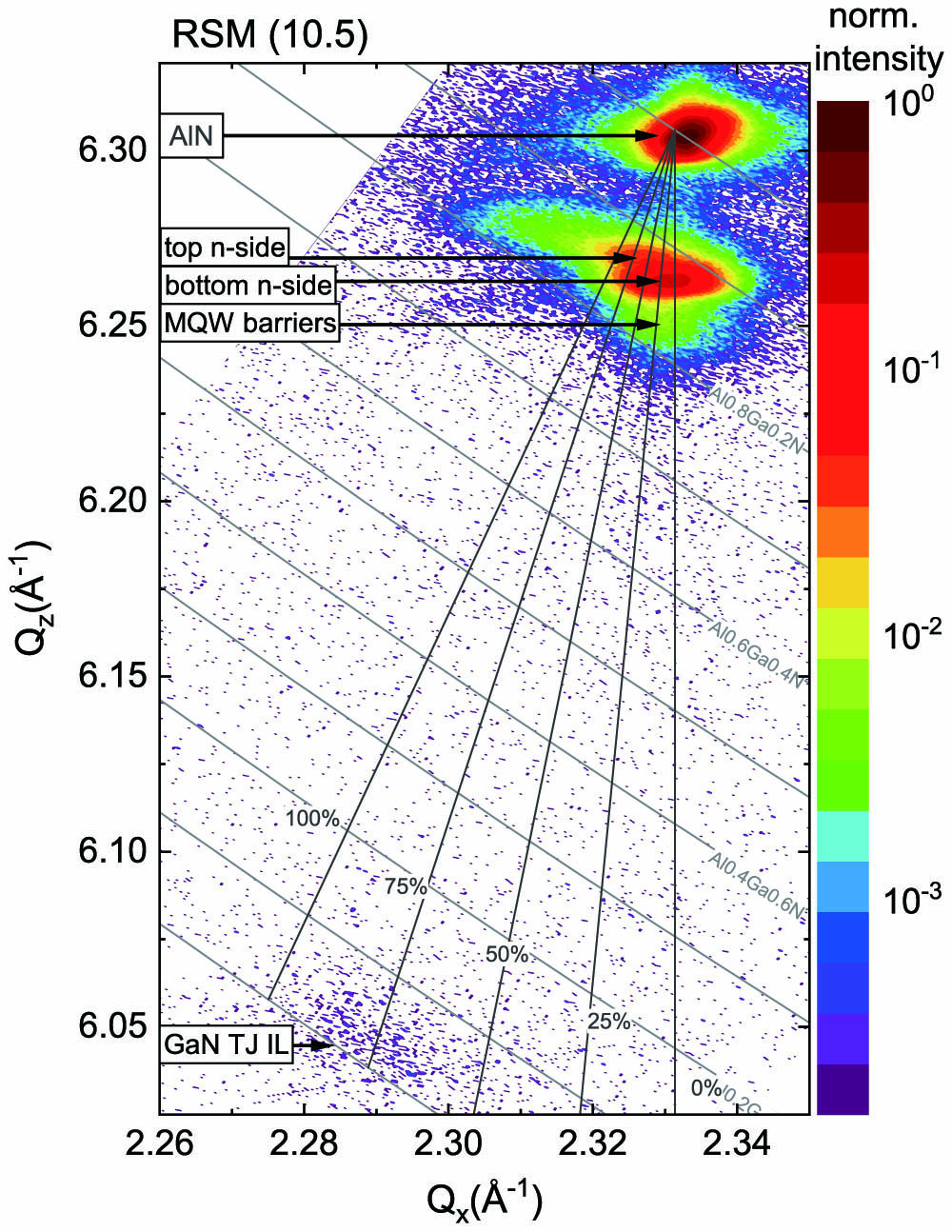
Figure 1.HR-XRD RSM near the AlN (10.5) reflex of a TJ LED heterostructure. Peaks corresponding to the individual layers are labeled in the graphic.
The electrical characteristics of the bottom and top current spreading layers and the n-contacts have been determined by linear transmission line method (TLM) measurements at a constant current density of due to the rectifying behavior [25]. Both n-contacts show rectifying characteristics as expected for such high Al mole fraction [8,23]. The sheet and contact resistivities of both layers are and , respectively, demonstrating that the electrical characteristics of the top layer are not influenced by the underlying Mg-doped layer grown before.
In order to determine the differential resistivity of the TJ LEDs, the IV characteristic has been measured on a mesa size of [see Fig. 4(a)] and dV/dj was calculated to be at a current density of . Figure 2 summarizes the differential resistivities reported in the literature of MBE- and MOVPE-grown AlGaN-based TJ LEDs as a function of the bandgap and the Al mole fraction at the TJ interface [15,18,26–35]. The lowest reported values are in the range for GaN TJ interfaces () at current densities between and and increase to the range for AlGaN TJ interfaces up to an Al mole fraction of () measured at a current density of . The relatively high resistivity presented here (which is an upper estimate due to the low current density) can be ascribed to the resistance occurring at the TJ interface due to an inefficient carrier tunneling into the large bandgap material ( for ). Additionally, high n-layer resistivities most likely contribute to the total differential resistivity [7,8,23]. However, the majority of the TJs reported in literature were grown by MBE, which might enable much more abrupt doping profiles at the TJ interface [17], potentially increasing the tunneling probabilities and lowering the differential resistivities.
![]()
Figure 2.Differential resistivity as a function of the bandgap and Al mole fraction at the TJ interface as reported for III-nitride LEDs [15,18,26
Figure 3 shows the on-wafer measured spectra of a TJ LED () in cw operation at 5 mA as measured through the bottom substrate (solid line) and through the top surface (dotted line) of the device. The peak emission wavelength is 232 nm with an FWHM of 11 nm and only slight parasitic luminescence contributions at longer wavelengths centered around 280 nm and 400 nm. The 280 nm luminescence can be attributed to Mg-related deep level transitions at the MQW to EBL interface [9], whereas the 400 nm luminescence might originate from donor-acceptor-pair recombinations at the highly Si-doped TJ interface or in the top or the bottom current spreading layer [22,36]. The inset of Fig. 3 shows a UV-sensitive EL microscopy image of a 232 nm TJ LED () with a square-shaped frame top n-contact at 5 mA. The luminescence intensity is relatively homogeneous over the entire emitting area, which indicates sufficient current spreading and spatially homogeneous tunneling. Additionally, some small areas show higher intensities (orange-red), which might be correlated with a change of the local LEE due to the presence of pits and surface hillocks as observed by scanning electron microscopy. However, as these surface defects can potentially also influence the carrier injection and, as the UV-sensitive camera is not wavelength selective, the origin of the high-intensity luminescence is subject to further investigation.
![]()
Figure 3.Spectral power density versus emission wavelength plot for a 232 nm TJ LED (
Figure 4(a) shows the on-wafer measured LIV characteristic and EQE of a TJ LED () with a stripe top n-contact measured through the bottom substrate (solid lines) and top surface (dashed lines). The operating voltage of the TJ LED is 26 V at 10 mA, which is significantly higher in comparison to a conventional LED with a non-transparent p-side (6.8 V at 10 mA) [8] and needs to be improved in order to achieve a high wall-plug efficiency (WPE). For emission through the bottom substrate, an emission power of 81 μW at 10 mA is measured (with the Si photodiode 3 mm below the LED). The emission power measured through the top surface at 10 mA is 13 μW (Si photodiode 10.5 mm above the LED). This translates into EQEs of 0.15% and 0.025% for bottom and top emission at 10 mA, respectively. As a comparison, a bottom emission power of 45 μW is obtained at 10 mA for a conventional LED [8]. Note that the given values for emission power are diminished by the detector cone sizes of the bottom and top emission EL setup, which can only detect light in detector half-cone angles of 61° and 28°, respectively. The strong increase in emission power in comparison to a conventional LED by nearly a factor of 2 can be attributed to the high transparency of the entire TJ LED heterostructure as well as the very high integrated reflection at the interface of 96% at 232 nm due to internal reflection, which results in a high bottom LEE (see also Fig. 6, left).
![]()
Figure 4.(a) LIV characteristics and EQE of a TJ LED measured through the bottom substrate (solid lines) and the top surface (dashed lines). Far-field emission pattern measured on-wafer of (b) the bottom and (c) the top hemispheres at a constant current of 5 mA. The black dashed lines in (b) and (c) indicate the detectable emission by the bottom and top EL setup as shown in (a).
To measure the integrated emission power of the TJ LEDs, far-field measurements have been carried out at a constant current of 5 mA in order to minimize device degradation [37]. Nevertheless, even at this low current, a degradation of the TJ LED emission power of approximately 10% was observed within one hour. The far fields of the bottom and the top hemispheres are shown in Figs. 4(b) and 4(c). Note that only half of the top hemisphere could be measured due to the sample holder and the power supply. The black dashed lines at 61° and 28° represent the detection cone sizes of the photodiode below and above the LED, respectively. Both far fields show a spherical Lambertian-like emission pattern with a maximum radiant intensity parallel to the -axis. This is caused by the TE-polarized portions of the emitted light as well as refraction and multiple reflection of the TM-polarized portions [12,23] at interfaces and at the ELO pattern of the AlN buffer. The maximum radiant intensity of the top hemisphere is , whereas the maximum radiant intensity of the bottom hemisphere is . Integrating the emission power of both hemispheres (assuming a symmetric top hemisphere) yields 77 μW at 5 mA (with 45 μW emitted toward the bottom and 32 μW emitted toward the top hemisphere), which correlates to an EQE of 0.29%.
From Monte Carlo ray-tracing simulations, the LEE of the TJ LEDs was determined to be 17.5% with 9.5% extracted in the bottom hemisphere and 8% extracted in the top hemisphere (see also Fig. 6, left). The difference in emission power and LEE of the bottom and top hemispheres is caused by higher Fresnel reflections at the top interface (AlGaN/air) of 20% in comparison to the bottom interfaces (AlGaN/AlN/sapphire/air) of 11%, different surface roughnesses of the top AlGaN and the bottom sapphire, and the ELO pattern. The ratio of the simulated top to bottom LEE is 0.84, which is in reasonable agreement with the ratio of the integrated top to bottom emission powers, which is 0.71. The discrepancy might be caused by degradation of the LEDs during far-field measurements (10% reduction for top emission far field) and potential light absorption within the GaN:Si TJ IL. Although transmission measurements of the entire TJ LED heterostructure (not shown here) do not show any indication of GaN-related light absorption around 360 nm, which is consistent with transmission measurements on 268 nm TJ LEDs with varied GaN:Si TJ IL thicknesses [18], and the GaN TJ IL is observable within the HR-XRD RSMs. Thus, the light absorption within the simulations of the LEE might be underestimated. Due to the high transparency of the heterostructures, we estimate the error of the LEE simulations to be approximately 6%.
As the heat removal through the sapphire substrate is very inefficient, flip-chip mounting is the most common solution for efficient heat extraction [37]. This requires the top metallization to cover the entire LED mesa and additionally to be highly reflective in order to redirect the light toward the substrate. However, the typically employed metal schemes such as V/Al or Ti/Al are not suitable as large-area top surface contacts, as they exhibit very low reflectivities. The material of choice for a reflector is aluminum, as it offers an integrated reflection at the interface at 232 nm of 94% (assuming an emission pattern from the active region with an in-plane DoP of [12]). However, aluminum is not a suitable low-resistance contact material to with high Al mole fraction. Therefore, due to the excellent current spreading in the top layer, the design of choice is a small-area annealed V/Al n-contact with low resistance combined with a large-area aluminum reflector with high reflectivity. As already mentioned, the integrated reflection at the interface at 232 nm is already very high (96%), and hence the main purpose of the top metallization is to minimize light absorption with a carefully designed metal scheme rather than to increase the bottom LEE and emission power.
Figure 5(a) shows the LIV characteristics and EQE measured through the bottom substrate of the same TJ LED device as presented in Fig. 4 after the deposition of the aluminum reflector. The operating voltage of 25 V at 10 mA is slightly lower in comparison to measurements without aluminum reflector. This might be attributed to a current flow over the large-area aluminum reflector. However, as the aluminum reflector has a much higher contact resistivity, the main current flow remains through the low-resistivity V/Al n-contact. The emission power measured through the bottom substrate at 10 mA is 84 μW, which correlates to an EQE of 0.16%. Again, this value is diminished due to the limited detector half-cone angle of 61°. The far-field measurements of the bottom hemisphere shown in Fig. 5(b) reveal an almost identical emission pattern as obtained without aluminum reflector with a maximum radiant intensity of parallel to the -axis. The integrated far-field emission power and EQE at 5 mA are 42 μW and 0.21%, respectively. Monte Carlo ray-tracing simulations of the TJ LEDs with aluminum reflector reveal a bottom LEE of 11% (see also Fig. 6, center).
![]()
Figure 5.(a) LIV characteristics and EQE of a TJ LED with an aluminum reflector on the top surface as measured through the bottom substrate. (b) Far-field emission pattern measured on-wafer of the bottom hemisphere at a constant current of 5 mA. The black dashed line indicates the detectable emission by the bottom EL setup as shown in (a).
![]()
Figure 6.Schematic TJ LED heterostructure and simulated LEE of (left) a TJ LED without aluminum reflector, (center) a TJ LED with large-area aluminum reflector, and (right) a TJ LED with large-area V/Al n-contact.
Despite the simulations of the bottom LEE showing an increase from 9.5% to 11% when depositing an aluminum reflector, experimentally a slight reduction of the integrated bottom emission power from 45 to 42 μW at 5 mA is observed. This reduction is most likely caused by device degradation due to the measurement order and time. A slight increase from 81 to 84 μW at 10 mA is observed when measured with the Si photodiode with limited detector half cone of 61° but negligible degradation. As comparison, depositing a large-area V/Al n-contact would lead to a reduction of the simulated bottom LEE to 4.5%, thus leading to an expected reduction of the emission power of more than 50%. This demonstrates that the design of a small-area annealed V/Al n-contact with low resistivity combined with a large-area aluminum reflector with a high reflectivity sufficiently avoids light absorption, which would be caused by different metallization schemes. Figure 6 depicts the simulated LEEs of a TJ LED without aluminum reflector (left), a TJ LED with large-area aluminum reflector (center), and a TJ LED with large-area annealed V/Al n-contact (right).
Finally, the performance limit of the same TJ LED device with aluminum reflector as presented in Fig. 4 and Fig. 5 has been tested by on-wafer EL measurements in cw operation until thermal rollover and in pulsed mode operation (pulse length of 2 μs, repetition rate of 20 kHz) through the bottom substrate (61° half-cone angle detectable). As shown in Fig. 7, in cw operation a maximum emission power of 220 μW is reached at 33 mA for an operating voltage of 28 V. A maximum EQE of 0.17% is reached at 16 mA. In pulsed mode operation, the effects of Joule heating are strongly reduced, and a maximum output power of 1.73 mW at 100 mA was achieved. A maximum EQE of 0.35% is obtained at a current of 50 mA. In comparison to recent literature [5,6,23,38,39], the EQE of the 232 nm TJ LED is similar to the highest reported data for conventional LED designs. Further improvements of the device performance can be expected by dicing and flip-chip mounting to enhance heat dissipation. However, the WPE needs to be improved by further optimizing the doping profile of the TJ interface and thus reducing the TJ resistance and operating voltage.
![]()
Figure 7.On-wafer measured bottom LIV characteristics in cw (solid lines) and pulsed mode operation (bullets) of a tunnel heterojunction LED (
4. CONCLUSION
In conclusion, we successfully demonstrated highly transparent tunnel heterojunction LEDs with a peak emission of 232 nm and tunnel injection into layers with a bandgap of 5.6 eV entirely grown by MOVPE. The on-wafer measured emission power and EQE of a device without reflector as determined by integrated far-field measurements at 5 mA are 77 μW and 0.29%, respectively. After deposition of a highly reflective aluminum reflector, a maximum emission power under pulsed mode operation of 1.73 mW at 100 mA and a maximum EQE of 0.35% at 50 mA measured through the bottom substrate have been presented. Currently, the operating voltage of the presented tunnel heterojunction LEDs is significantly higher in comparison to conventional LEDs, thus limiting the WPE. However, further improvements of the TJ growth conditions can lead to an LED design that utilizes highly transparent heterostructures combined with the deposition of a highly reflective aluminum reflector and at the same time maintaining a high hole injection efficiency.
Acknowledgment
Acknowledgment. The authors thank Sylvia Hagedorn and Markus Weyers (FBH, Berlin) for providing the ELO AlN/sapphire and for critically reading the paper, as well as Praphat Sonka (TU Berlin) for technical assistance.
References
[1] J. Mellqvist, H. Axelsson, A. Rosén. DOAS for flue gas monitoring—III.
[2] J. Hodgkinson, R. P. Tatam. Optical gas sensing: a review. Meas. Sci. Technol., 24, 012004(2013).
[3] M. Degner, H. Ewald. UV emitters in gas sensing applications. III-Nitride Ultraviolet Emitters, 321-349(2016).
[4] F. Mehnke, M. Guttmann, J. Enslin, C. Kuhn, C. Reich, J. Jordan, S. Kapanke, A. Knauer, M. Lapeyrade, U. Zeimer, H. Krüger, M. Rabe, S. Einfeldt, T. Wernicke, H. Ewald, M. Weyers, M. Kneissl. Gas sensing of nitrogen oxide utilizing spectrally pure deep UV LEDs. IEEE J. Sel. Top. Quantum Electron., 23, 29-36(2017).
[5] M. Kneissl, T.-Y. Seong, J. Han, H. Amano. The emergence and prospects of deep-ultraviolet light-emitting diode technologies. Nat. Photonics, 13, 233-244(2019).
[6] H. Amano, R. Collazo, C. D. Santi, S. Einfeldt, M. Funato, J. Glaab, S. Hagedorn, A. Hirano, H. Hirayama, R. Ishii, Y. Kashima, Y. Kawakami, R. Kirste, M. Kneissl, R. Martin, F. Mehnke, M. Meneghini, A. Ougazzaden, P. Parbrook, S. Rajan, P. Reddy, F. Römer, J. Ruschel, F. Scholz, L. Schowalter, P. Shields, Z. Sitar, L. Sulmoni, T. Wang, T. Wernicke, M. Weyers, B. Witzigmann, Y.-R. Wu, T. Wunderer, Y. Zhang. The 2020 UV emitter roadmap. J. Phys. D, 53, 503001(2020).
[7] F. Mehnke, T. Wernicke, H. Pingel, C. Kuhn, C. Reich, V. Kueller, A. Knauer, M. Lapeyrade, M. Weyers, M. Kneissl. Highly conductive n-Al
[8] L. Sulmoni, F. Mehnke, A. Mogilatenko, M. Guttmann, T. Wernicke, M. Kneissl. Electrical properties and microstructure formation of V/Al-based n-contacts on high Al mole fraction n-AlGaN layers. Photon. Res., 8, 1381-1387(2020).
[9] F. Mehnke, C. Kuhn, M. Guttmann, C. Reich, T. Kolbe, V. Kueller, A. Knauer, M. Lapeyrade, S. Einfeldt, J. Rass, T. Wernicke, M. Weyers, M. Kneissl. Efficient charge carrier injection into sub-250 nm AlGaN multiple quantum well light emitting diodes. Appl. Phys. Lett., 105, 051113(2014).
[10] T. A. Henry, A. Armstrong, A. A. Allerman, M. H. Crawford. The influence of Al composition on point defect incorporation in AlGaN. Appl. Phys. Lett., 100, 043509(2012).
[11] R. G. Banal, M. Funato, Y. Kawakami. Optical anisotropy in [0001]-oriented Al
[12] M. Guttmann, F. Mehnke, B. Belde, F. Wolf, C. Reich, L. Sulmoni, T. Wernicke, M. Kneissl. Optical light polarization and light extraction efficiency of AlGaN-based LEDs emitting between 264 and 220 nm. Jpn. J. Appl. Phys., 58, SCCB20(2019).
[13] N. Susilo, J. Enslin, L. Sulmoni, M. Guttmann, U. Zeimer, T. Wernicke, M. Weyers, M. Kneissl. Effect of the GaN:Mg contact layer on the light-output and current-voltage characteristic of UVB LEDs. Phys. Status Solidi A, 215, 1700643(2018).
[14] M. Jo, N. Maeda, H. Hirayama. Enhanced light extraction in 260 nm light-emitting diode with a highly transparent p-AlGaN layer. Appl. Phys. Express, 9, 012102(2015).
[15] Y. Zhang, S. Krishnamoorthy, F. Akyol, S. Bajaj, A. A. Allerman, M. W. Moseley, A. M. Armstrong, S. Rajan. Tunnel-injected sub-260 nm ultraviolet light emitting diodes. Appl. Phys. Lett., 110, 201102(2017).
[16] S. Okawara, Y. Aoki, M. Kuwabara, Y. Takagi, J. Maeda, H. Yoshida. Nitride-based stacked laser diodes with a tunnel junction. Appl. Phys. Express, 11, 012701(2018).
[17] I. P. Smorchkova, E. Haus, B. Heying, P. Kozodoy, P. Fini, J. P. Ibbetson, S. Keller, S. P. DenBaars, J. S. Speck, U. K. Mishra. Mg doping of GaN layers grown by plasma-assisted molecular-beam epitaxy. Appl. Phys. Lett., 76, 718-720(2000).
[18] C. Kuhn, L. Sulmoni, M. Guttmann, J. Glaab, N. Susilo, T. Wernicke, M. Weyers, M. Kneissl. MOVPE-grown AlGaN-based tunnel heterojunctions enabling fully transparent UVC LEDs. Photon. Res., 7, B7-B11(2019).
[19] S. Zhao, S. M. Sadaf, S. Vanka, Y. Wang, R. Rashid, Z. Mi. Sub-milliwatt AlGaN nanowire tunnel junction deep ultraviolet light emitting diodes on silicon operating at 242 nm. Appl. Phys. Lett., 109, 201106(2016).
[20] S. Rajan, T. Takeuchi. III-Nitride Tunnel Junctions and Their Applications(2017).
[21] A. Knauer, A. Mogilatenko, S. Hagedorn, J. Enslin, T. Wernicke, M. Kneissl, M. Weyers. Correlation of sapphire off-cut and reduction of defect density in MOVPE grown AlN. Phys. Status Solidi B, 253, 809-813(2016).
[22] G. Kusch, M. Nouf-Allehiani, F. Mehnke, C. Kuhn, P. R. Edwards, T. Wernicke, A. Knauer, V. Kueller, G. Naresh-Kumar, M. Weyers, M. Kneissl, C. Trager-Cowan, R. W. Martin. Spatial clustering of defect luminescence centers in Si-doped low resistivity Al0.82Ga0.18N. Appl. Phys. Lett., 107, 072103(2015).
[23] F. Mehnke, L. Sulmoni, M. Guttmann, T. Wernicke, M. Kneissl. Influence of light absorption on the performance characteristics of UV LEDs with emission between 239 and 217 nm. Appl. Phys. Express, 12, 012008(2019).
[24] Y. Kuwano, M. Kaga, T. Morita, K. Yamashita, K. Yagi, M. Iwaya, T. Takeuchi, S. Kamiyama, I. Akasaki. Lateral hydrogen diffusion at p-GaN layers in nitride-based light emitting diodes with tunnel junctions. Jpn. J. Appl. Phys., 52, 08JK12(2013).
[25] B. B. Haidet, B. Sarkar, P. Reddy, I. Bryan, Z. Bryan, R. Kirste, R. Collazo, Z. Sitar. Nonlinear analysis of vanadium- and titanium-based contacts to Al-rich n-AlGaN. Jpn. J. Appl. Phys., 56, 100302(2017).
[26] D. Takasuka, Y. Akatsuka, M. Ino, N. Koide, T. Takeuchi, M. Iwaya, S. Kamiyama, I. Akasaki. GaInN-based tunnel junctions with graded layers. Appl. Phys. Express, 9, 081005(2016).
[27] Y. Akatsuka, S. Iwayama, T. Takeuchi, S. Kamiyama, M. Iwaya, I. Akasaki. Doping profiles in low resistive GaN tunnel junctions grown by metalorganic vapor phase epitaxy. Appl. Phys. Express, 12, 025502(2019).
[28] Y. Zhang, S. Krishnamoorthy, J. M. Johnson, F. Akyol, A. Allerman, M. W. Moseley, A. Armstrong, J. Hwang, S. Rajan. Interband tunneling for hole injection in III-nitride ultraviolet emitters. Appl. Phys. Lett., 106, 141103(2015).
[29] Y. Zhang, S. Krishnamoorthy, F. Akyol, A. A. Allerman, M. W. Moseley, A. M. Armstrong, S. Rajan. Design and demonstration of ultra-wide bandgap AlGaN tunnel junctions. Appl. Phys. Lett., 109, 121102(2016).
[30] Y. Zhang, Z. Jamal-Eddine, F. Akyol, S. Bajaj, J. M. Johnson, G. Calderon, A. A. Allerman, M. W. Moseley, A. M. Armstrong, J. Hwang, S. Rajan. Tunnel-injected sub 290 nm ultra-violet light emitting diodes with 2.8% external quantum efficiency. Appl. Phys. Lett., 112, 071107(2018).
[31] S. Krishnamoorthy, F. Akyol, P. S. Park, S. Rajan. Low resistance GaN/InGaN/GaN tunnel junctions. Appl. Phys. Lett., 102, 113503(2013).
[32] S. Krishnamoorthy, F. Akyol, S. Rajan. InGaN/GaN tunnel junctions for hole injection in GaN light emitting diodes. Appl. Phys. Lett., 105, 141104(2014).
[33] E. C. Young, B. P. Yonkee, F. Wu, S. H. Oh, S. P. DenBaars, S. Nakamura, J. S. Speck. Hybrid tunnel junction contacts to III-nitride light-emitting diodes. Appl. Phys. Express, 9, 022102(2016).
[34] M. Malinverni, D. Martin, N. Grandjean. InGaN based micro light emitting diodes featuring a buried GaN tunnel junction. Appl. Phys. Lett., 107, 051107(2015).
[35] V. F. Arcara, B. Damilano, G. Feuillet, S. Vézian, K. Ayadi, S. Chenot, J.-Y. Duboz. Ge doped GaN and Al0.5Ga0.5N-based tunnel junctions on top of visible and UV light emitting diodes. J. Appl. Phys., 126, 224503(2019).
[36] K. B. Nam, M. L. Nakarmi, J. Y. Lin, H. X. Jiang. Deep impurity transitions involving cation vacancies and complexes in AlGaN alloys. Appl. Phys. Lett., 86, 222108(2005).
[37] J. Glaab, J. Ruschel, F. Mehnke, M. Lapeyrade, M. Guttmann, T. Wernicke, M. Weyers, S. Einfeldt, M. Kneissl. Degradation behavior of AlGaN-based 233 nm deep-ultraviolet light emitting diodes. Semicond. Sci. Technol., 33, 095017(2018).
[38] A. Yoshikawa, R. Hasegawa, T. Morishita, K. Nagase, S. Yamada, J. Grandusky, J. Mann, A. Miller, L. J. Schowalter. Improve efficiency and long lifetime UVC LEDs with wavelengths between 230 and 237 nm. Appl. Phys. Express, 13, 022001(2020).
[39] N. Lobo-Ploch, F. Mehnke, L. Sulmoni, H. K. Cho, M. Guttmann, J. Glaab, K. Hilbrich, T. Wernicke, S. Einfeldt, M. Kneissl. Milliwatt power 233 nm AlGaN-based deep UV-LEDs on sapphire substrates. Appl. Phys. Lett., 117, 111102(2020).

Set citation alerts for the article
Please enter your email address
© Copyright 2018-2021 | Chinese Laser Press. All Rights Reserved 沪ICP备15018463号-20