
Kui Zhou, Zheng Shan, Qian Zhang, Xiejun Wang, Jian Zhou, Chenwei Deng, Yiting Yu. Research Progresses of MEMS Fabry-Perot Filtering Chips and Their Applications for Spectral Detection[J]. Acta Optica Sinica, 2022, 42(8): 0800001
- Acta Optica Sinica
- Vol. 42, Issue 8, 0800001 (2022)
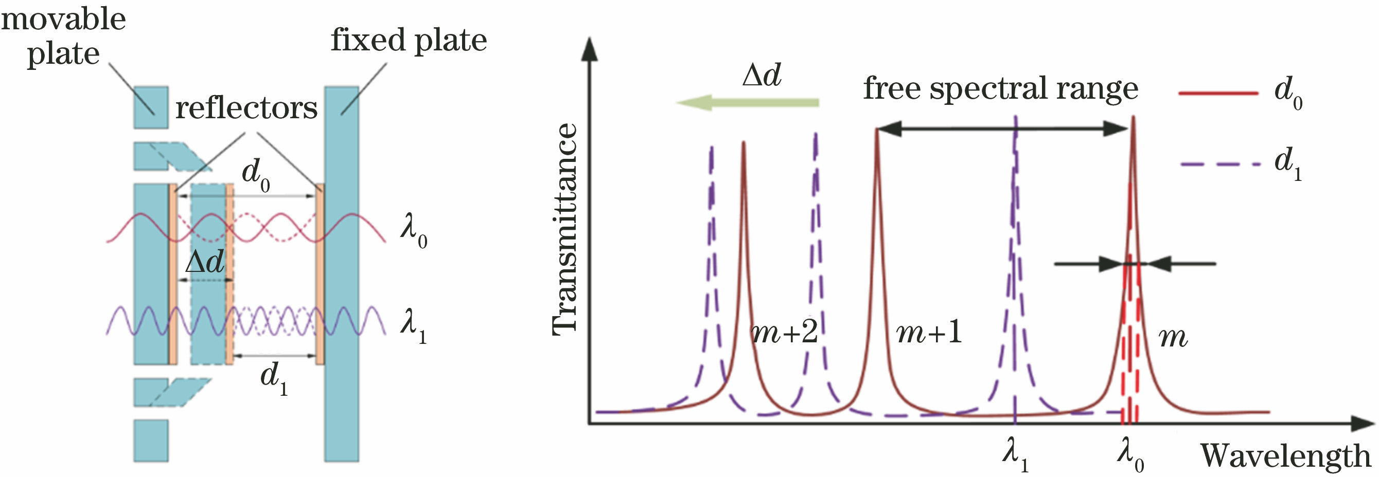
Fig. 1. Basic structure and working principle of MEMS-FP filtering chips
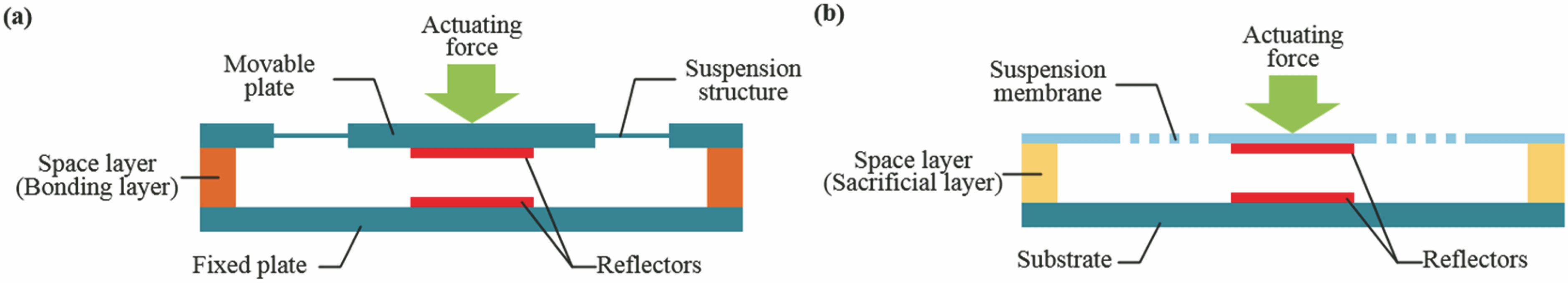
Fig. 2. Comparison of MEMS-FP filtering chips based on bulk micromachining and surface micromachining. (a) Bulk micromachining; (b) surface micromachining
Fig. 3. MEMS-FP filtering chips based on different actuation strategies. (a) Electrostatic actuation[45]; (b) piezoelectric actuation[52]; (c) thermal actuation[53]; (d) electromagnetic actuation[54]
Fig. 4. Reflectance of different metallic films with different thicknesses. (a) Au film; (b) Ag film; (c) Al film
Fig. 5. Reflectance of DBR with different film compositions. (a) Schematic structure; (b) TiO2/SiO2 film; (c) TiO2/Al2O3 film
Fig. 6. Phase shift of MEMS-FP filtering chip based on DBR
Fig. 7. Photonic-crystal reflector based on sub-wavelength periodic hole-array[60]. (a) Schematic structure; (b) SEM picture; (c) measured reflectance
Fig. 8. Electrostatically tunable MEMS-FP filtering chip working in mid-infrared wavelength developed by NASA in US[62]
Fig. 9. Electrostatically tunable MEMS-FP filtering chip working in visible wavelength and spectral imaging system developed by US Army Research Laboratory[64-66]
Fig. 10. Infrared MEMS-FP filtering chip and tunable pyroelectric detector[68]. (a) Schematic structure; (b) optical performance; (c) tunable pyroelectric detector
Fig. 11. Dual-band MEMS-FP filtering chip and detector module[43,70-72]. (a) Schematic structure and spectral performance of filtering chip; (b) optical design and assemble process of detector module
Fig. 12. Visible light MEMS-FP filtering chip based on Si3N4 film[73]. (a) Schematic structure and working principle; (b) filtering chips with different aperture size; (c) optical performance
Fig. 13. MEMS-FP filtering chip based on photonic-crystal reflector[75]
Fig. 14. Surface-machined MEMS-FP filtering chip working in visible light[78]
Fig. 15. Surface-machined MEMS-FP filtering chip based on Ag mirror[83]
Fig. 16. Piezo-actuated MEMS-FP filtering chip series developed by VTT[77]
Fig. 18. Spectral sensor for mobile gas detection[87]
Fig. 19. Spectral imaging module assembled with iPhone 5s[88]
Fig. 21. Hand-held spectral detection systems based on MEMS-FP filtering chips[81]. (a) Hand-held spectral imager[94]; (b) miniaturized spectral imager[95]; (c) point source type miniaturized spectrometer
Fig. 22. MEMS-FP filtering chips developed by domestic different research institutes. (a)(b) Shanghai Institute of Microsystem and Information Technology, Chinese Academy of Sciences[96-97]; (c)(d) Huazhong University of Science and Technology[98-99]
Fig. 23. Electromagnetic actuation MEMS-FP filtering chips and miniature spectral imagers applied to different wavebands developed by Northwestern Polytechnical University. (a) Visible light waveband;(b) long-wave infrared waveband
Fig. 24. Common optical materials and their properties. (a) Transmission range; (b) transmittance of typical infrared optical materials
Fig. 25. MEMS-FP filtering structures based on GST phase-change material. (a) FP tunable filtering structure[104]; (b) metasurface filtering structure[105]
|
Table 1. Comparison of MEMS-FP filtering chips based on bulk micromachining and surface micromachining
|
Table 2. Performance comparison of MEMS-FP filtering chips based on different actuation strategies
|
Table 3. Characteristic comparison of metallic mirror and DBR

Set citation alerts for the article
Please enter your email address
© Copyright 2018-2021 | Chinese Laser Press. All Rights Reserved 沪ICP备15018463号-20