
Jiaxin Liu, Xiyuan Tang, Linxiao Shen, Shaolan Li, Zhelu Li, Wenjuan Guo, Nan Sun. Error suppression techniques for energy-efficient high-resolution SAR ADCs[J]. Journal of Semiconductors, 2020, 41(11): 111403
- Journal of Semiconductors
- Vol. 41, Issue 11, 111403 (2020)
Abstract
1. Introduction
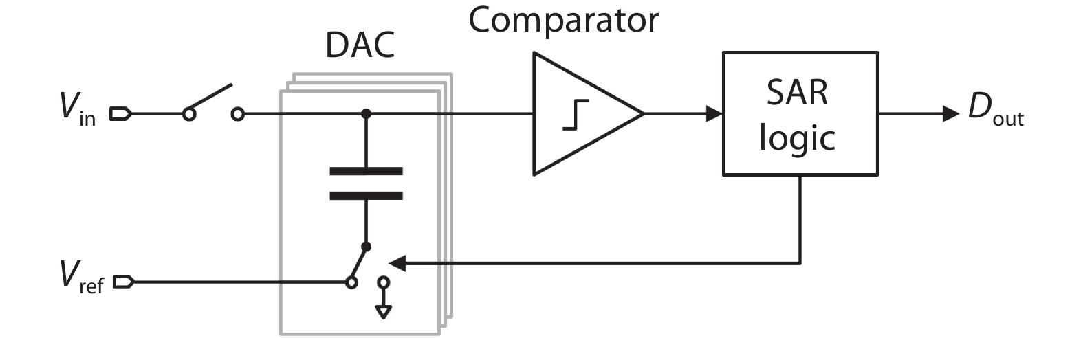
As the interface between the analog world and the digital world, the analog-to-digital converter (ADC) plays a key role in many electronics systems. In recent years, the boom of internet-of-things (IoTs) is driving the world into an unprecedented scale of connectivity and ubiquitous sensing. The fast-growing number of sensing nodes pose stringent requirements on energy efficiency of ADCs. Among various existing architectures, the successive approximation register (SAR) is deemed to be a promising candidate for ADC designs. Fig. 1 is the generic block diagram of a SAR ADC. Although most SAR ADCs are differentially implemented, a single-end one is shown here for simplicity. It consists of a capacitor digital-to-analog converter (DAC), a comparator and a SAR logic. Owing to the simple and mostly digital implementation, the SAR ADC is highly scaling friendly, and can achieve high speed and low power in an advanced nanometer CMOS technology.
![]()
Figure 1.Generic block diagram of a SAR ADC.
However, on top of the stringent power efficiency requirement, many emerging applications also have an increasing demand for high ADC resolution. This is because a high resolution ADC provides tolerance to strong interferences, such as the blocker signals in receivers and the motion artifacts in sensors. Nevertheless, in the context of SAR ADC, it is very challenging to achieve the high resolution while maintaining the superior energy efficiency. This is mainly limited by several circuit errors, including the sampling kT/C noise, comparator noise, and DAC mismatch.
Recently, there is a trend to expand the superior energy efficiency of SAR ADC to the high-resolution domain. Various emerging efforts have been made in the past decade. The key of these efforts is to leverage the technology scaling and to suppress the circuit errors in an efficient way. This paper presents a review on three classes of emerging error suppression techniques, including the kT/C noise reduction, the noise-shaping (NS) SAR, and the DAC mismatch error shaping (MES), for realizing energy-efficient high-resolution SAR ADCs. This paper is organized as follows. Section 2 provides an analysis on the major error sources. From Section 3 to Section 5, three error suppression techniques are introduced, respectively. Section 6 concludes this paper.
2. Error sources in SAR ADC
There are various error sources that can degrade the accuracy of a SAR ADC. Among them, some errors do not make up the bulk of the total error and can be suppressed with small costs. Several examples are as follows. The quantization error can be halved by adding one more bit, the hardware overhead is small. The DAC noise can be minimized by reducing the switch resistance, and this becomes easier with a more advanced technology. The sampling non-linearity can be mitigated by using bootstrapped switches. However, some other errors are very hard to be addressed and can become the limiting factors in a SAR ADC, such as the sampling kT/C noise, the comparator noise, and the DAC mismatch. This section reviews these major errors and provides a comprehensive understanding on the energy efficiency and resolution limitations.
2.1. Sampling kT/C noise
The kT/C noise occurs in any ADC with a sample-and-hold (S/H) circuit. It comes from the thermal noise associated with the sampling switch. A sampling circuit with kT/C noise is shown in Fig. 2. When the sampling switch is on, the input signal is tracked on the sampling capacitor. At the same time, the sampling switch with an equivalent resistance of Ron generates thermal noise at the top plate of the capacitor. Once the sampling switch turns off, both the input signal and the switch noise are frozen on the capacitor. The switch noise corrupts the input signal, degrading the signal-to-noise ratio (SNR) of the sampling circuit.
![]()
Figure 2.A sampling circuit with
The noise spectrum of the sampling switch at on state is white, its power spectrum density (PSD) is 4kTRon. The switch resistance and the sampling capacitor form a RC low-pass filter, limiting the noise bandwidth. By integrating the noise in the frequency domain, we can calculate the total sampling noise is
It shows that the sampling noise is independent of the switch resistance and is solely determined by the capacitor. To reduce the sampling noise, the only way is to increase the capacitor C but it is at the cost of increased power, area, and design efforts for not only the SAR ADC core, but also its input driver and reference buffer.
2.2. Comparator noise
The comparator converts the analog input into digital output, and is a key building block in SAR ADCs. Its power, noise, and speed largely determine the SAR ADC’s performance. A comparator consists of a preamp that enlarges the input signal, followed by a latch to resolve the final decision.
The conventional comparator design adopts an active preamp which consumes static power. To save the power, dynamic comparators are developed. The Strong-ARM latch[
![]()
Figure 3.Strong-ARM latch[
where vn,preamp and vn,latch represent the noise contributions of the preamp and the latch, respectively, and A is the preamp gain. As analyzed in Ref. [2], the preamp noise can be expressed as
where Cx is the loading capacitor of the preamp, Vthp and Vthn are the threshold voltages of PMOS and NMOS transistors, respectively. The noise from the latch can be expressed as
where γ is the is the device-dependent fitting parameter, and its theoretical value is 2/3 for long-channel devices. Co is the loading capacitor of the latch, it is not shown in Fig. 3.
To realize a low-noise comparator, one can apply the brute-force analog scaling, which is to increase the preamp gain, gm/ID and loading capacitors at the cost of increased power and transistor size. Generally, it requires 4 times of power for every 6 dB noise reduction, which is a steep power-noise trade-off. Moreover, the increased transistor size introduces large comparator input capacitance. It can cause signal attenuation at the comparator input, leading to increased ADC input referred noise.
2.3. DAC mismatch
DAC mismatch causes inconsistency between the analog weights of DAC cells and their digital weights. Fig. 4(a) shows the operation of a SAR ADC with a 12-bit DAC, C11–C0. In the sampling phase, the input signal is sampled on the DAC top plate and all the digital codes reset. In the conversion phase, the DAC cells are switched sequentially based on a binary search algorithm and their analog weights are subtracted from the DAC to bring the voltage at DAC top plate down to 0. At the same time, the digital output is established from 0 by assembling all the digital weights. In an ideal case, the DAC cells values, 211C–20C, perfectly match their digital weights, 211–20, and therefore the digital output represents the input signal accurately.
![]()
Figure 4.A SAR ADC with DAC mismatch: (a) operation scheme, (b) behavioral operation model.
In a practical design, each DAC cell deviates from its ideal value due to process variations. Without affecting the linearity, the most significant bit (MSB) cell C11 can be used as a reference to define the mismatch error of other DAC cells, as expressed in the following
where ei is the mismatch error of Ci.
Based on the definition above, the SAR ADC operation in Fig. 4(a) can be modeled behaviorally as depicted in Fig. 4(b). Firstly, the MSB cell is switched and its analog weight, DACMSB, is subtracted from the input. Then, the LSB cells are switched sequentially and the sum of their analog weights, DACLSBs, is subtracted from the input. Along with the subtraction of DACLSBs, the mismatch errors of the LSB cells, e10–e0, are also weighted and subtracted from the input. After digital weight assembly, the digital output is obtained as
The DAC mismatch error, E, is a combination of e10–e0 and the their corresponding LSB codes, and can be expressed as
As shown in Eq. (7), the DAC mismatch error is modulated by the digital output codes. Thereby, it is correlated with the input signal, and can cause non-linear distortions. The DAC mismatch issue is often the linearity bottleneck for high resolution ADCs.
3. Sampling kT/C noise reduction
The sampling kT/C noise has long been considered as a fundamental SNR limit for any ADC with a front-end S/H circuit. To satisfy the SNR requirement, the kT/C noise is typically suppressed by increasing the input capacitor size. The large input capacitors make it very costly to design the ADC input driver and reference buffer. Their power, area, and design complexity are typically much higher than the SAR ADC itself. To ease the ADC driver requirement while enabling high resolution, recently several emerging techniques are proposed to break the fundamental kT/C noise limit. In this session, three sampling kT/C noise reduction techniques that address the kT/C noise issue from different perspectives will be introduced.
3.1. Continuous-time SAR
In Ref. [3], Shen et al. demonstrated a 13-bit two-step SAR ADC with only 120 fF total input capacitance, as shown in Fig. 5. The key idea of this work is that it uses a continuous-time (CT) SAR as the first stage of the ADC. Since the sampling operation is removed in the CT SAR, the associated sampling kT/C noise is eliminated. Therefore, small input capacitors can be used but without incurring kT/C noise, greatly reducing the design cost for the ADC input driver. Because the input various with time, a CT SAR produces a tracking error, which makes it hard for a standalone CT SAR to go beyond the 10-bit resolution. To increase the overall ADC resolution, a two-step (or pipelined) architecture can be adopted. The CT SAR only needs to resolve a few bits (e.g., 6-bit), and its residue voltage is amplified by an inter-stage gain and then quantized by a second-stage discrete-time (DT) SAR. The DT SAR introduces a kT/C noise, but it is attenuated by the inter-stage gain when referred to the input.
![]()
Figure 5.Two-step SAR ADC with a continuous-time first stage[
However, the CT SAR approach suffers from several limitations. First, it cannot convert a DC signal since its input is AC coupled, limiting its application space. Second, the input signal frequency is limited to only 1 MHz to prevent large tracking errors from the CT SAR. Last, the CT SAR operation has to be very fast. Each CT SAR cycle is only 500 ps. Even though the input capacitor size is reduced, ensuring settling within such a short time can still be a challenge for the ADC input driver and reference buffer.
3.2. kT/C noise cancellation
Unlike Ref. [3] that eliminates the kT/C noise by removing the sampling operation in the front-end stage, another work by Liu et al.[
The SAR ADC with kT/C noise cancellation technique[
![]()
Figure 6.SAR ADC with
Compared with the prior kT/C noise reduction work[
3.3. Decoupling noise PSD and bandwidth
In Ref. [11], Li et al. explored another angle to tackle the kT/C noise issue. As discussed in Section 2.1, kT/C noise is a fundamental error source since its PSD and bandwidth are tightly coupled. To break the kT/C noise limit, this work proposed to decouple the noise PSD and bandwidth. This is realized by a two-stage amplifier-based sampling circuit, as shown in Fig. 7.
![]()
Figure 7.
Assuming gm1RL < < 1, the input referred noise PSD is dominated by the amplifier in the first stage, it can be expressed as
where gm1 is the transconductance of first-stage amplifier. By placing the dominant pole at the output of the second-stage amplifier, the noise bandwidth can be expressed as
where gm2 is the transconductance of second-stage amplifier, and RL is the output resistance of the first-stage amplifier. From Eqs. (8) and (9), the resulted total sampling noise power can be obtained as
It shows that the one can break the kT/C noise limit by setting gm2RL < 1.
An issue with this technique is that it decreases the tracking bandwidth (gm1gm2RL/2πC) by using a small gm2RL. To address this issue, a switching bandwidth technique is applied in the second-stage amplifier to maintain a high average tracking BW while achieving sampling noise bandwidth reduction. The input signal tracking is mostly done during the high bandwidth phase in which gm2RL is set to be 1. The sampling noise is reduced during the low bandwidth phase in which gm2RL is set to be less than 1.
4. Noise-shaping (NS) SAR
The comparator noise is a major limiting factor that prevents the SAR ADCs from achieving a high resolution. Traditionally, the delta-sigma (ΔΣ) architecture is commonly employed to realize high-resolution ADCs, since it can effectively suppress the comparator noise by noise shaping. However, the ΔΣ ADCs require high-performance operational transconductance amplifiers (OTAs), which are power-hungry and scaling unfriendly. To combine the benefits of both SAR and ΔΣ ADCs while obviating their drawbacks, several recent works proposed the concept of NS SAR ADCs[
![]()
Figure 8.Generic block diagram of a NS- SAR ADC.
The noise suppression capability of a NS-SAR ADC is determined by its noise transfer function (NTF). Assuming the first-order noise-shaping implementation, the NTF can be expressed as
where p is the zero of the NTF and is also the pole of the noise-shaping filter, 0 < p <1. The value of p reflects the effectiveness of noise shaping. With a larger p, the zero of NTF will be placed closer to the unit circle, and thus enabling a sharper noise-shaping effect.
To realize a NS-SAR ADC with high efficiency, the key is the design of the noise-shaping filter, which is expected to provide strong noise suppression, and at the same time, to be low power, scaling friendly and robust. Categorized by the implementation of noise-shaping filters, generally there are three types of NS-SAR ADCs, i.e., the close-loop amplifier-based one, the open-loop amplifier-based one and the passive one. In the following, the three categories of NS-SAR ADCs will be covered with insightful discussions on their benefits and limitations.
4.1. Close-loop amplifier-based NS-SAR
The first NS-SAR ADC design[
![]()
Figure 9.NS-SAR ADC with close-loop amplifier-based noise-shaping filter[
To improve the resolution of NS-SAR ADCs, Shu et al.[
To address the above limitations, Tang et al.[
![]()
Figure 10.Closed-Loop Dynamic Amplifier-based noise-shaping filter[
4.2. Open-loop amplifier-based NS-SAR
To improve the power-efficiency of NS-SAR ADCs, some researchers proposed to use open-loop amplifiers to realize the noise-shaping filters[
Fig. 11 shows the open-loop amplifier-based NS-SAR in Ref. [16], presented by Liu and Huang. Instead of using the classic active amplifier, this work uses a dynamic amplifier, further improving the power efficiency. A FIR-IIR loop filter is implemented to provide a sharp NTF. Both the FIR and IIR filters are realized by fully switched-capacitor methods. The dynamic amplifier is placed at the front-end of the loop filter, providing the gain to compensate for the signal attenuation during the passive charge sharing. It also effectively suppresses the noise from the back-end stages, allowing small capacitors to be used in the FIR and IIR filters for better area and speed.
![]()
Figure 11.Open-loop dynamic amplifier-based NS-SAR[
The NS-SAR ADCs discussed so far are all based on the cascaded-integrator-feed-forward (CIFF) structure. A limitation of the CIFF structure is that the NTF zero location directly associates with the filter quality, leading to a steep trade-off between noise-shaping effect and power efficiency. To overcome the limitation of CIFF structure, researchers proposed the error feedback (EF) structure[
![]()
Figure 12.NS-SAR ADC with EF structure and open-loop dynamic amplifier[
Nevertheless, using open-loop amplifiers brings the drawback of PVT sensitivity. The gain of an open-loop amplifier is sensitive to PVT variations, hurting the robustness of the overall ADC. In Ref. [16], the gain is adjusted by tuning the discharging currents. However, this method may not be suitable for volume production. The work of Ref. [17] ensures the gain robustness of the dynamic amplifier by using a background calibration, but this increases the design complexity. Moreover, background calibration requires a large number of input samples to process before convergence. It only works for continuous measurements. It is not suitable for IoT applications when the ADC stays in the hibernation mode most of the time, and needs to produce an accurate conversion result immediately after wake-up. In Refs. [18, 19], the gain variations are tolerated by placing the nominal NTF zeros far away from the unit circle, with a sacrifice of the noise shaping effect.
4.3. Passive NS-SAR
The above discussions show that both the close-loop and open-loop amplifier-based approaches suffer drawbacks from their amplifiers. To avoid these drawbacks, several researchers proposed to remove the amplifiers and use only switches and capacitors to build fully passive filters[
The first passive NS-SAR ADC was presented by Chen et al. in Ref. [20]. However, it only realizes a small NTF zero of 0.5 due to the lack of effective gain, leading to a mild noise shaping effect. To improve the shaping effect, Guo et al. proposed to employ multi-input-pair comparators to provide the required gain ratios in the loop filters, and they realized the first-order[
![]()
Figure 13.(a) Simplified core schematic and (b) 3-input-pair comparator of the second-order NS-SAR ADC[
However, the passive NS-SAR approach comes with the problem of poor thermal noise suppression as the passive loop filter does not produce effective gain. The thermal noise comes from two sources. First, the residue sampling and passive integration introduce a large kT/C noise. Second, the multi-input-pair comparator is much noisier than the standard 1-input-pair one. In the work of Ref. [22], the total kT/C noise of the passive loop filter in terms of in-band PSD is 18kT/CDAC, and the comparator input referred noise is 21 times larger than that of the 1-input-pair one. Although the passive NS-SAR ADC is hardware efficient, the large thermal noise harms its resolution and power efficiency. The thermal noise issue is alleviated in an optimized second-order passive NS-SAR proposed by Liu et al. in Ref. [23]. This work gets rid of the residue sampling on C0 and directly performs the integrations. By doing so, the total kT/C noise is reduced by 5 times, and the comparator input referred noise is reduced by more than 40%, compared with Ref. [22].
Seeking to improve the thermal noise suppression capability of passive NS-SAR ADCs, a few works tried to implement the effective gain in the passive loop filters. In Refs. [24, 25], the passive filters with 2 times passive gain were realized. They use no amplifier but just several additional switches, leading to very low hardware complexity. The passive gain of Ref. [24] is realized in the charge pump manner. At the end of the SAR conversion, two capacitors are connected in parallel with the DAC to perform the passive integration. After the integration, the two capacitors are stacked in series, boosting the integration voltage by 2 times. The work of Ref. [25] implements the 2 times passive gain by performing differential sampling. Moreover, it stacks the integration capacitor over the DAC, realizing the passive summation. The issue of Ref. [24] is that it still needs a multi-input-pair comparator for the summation, resulting in the large comparator noise. Although the work of Ref. [25] obviates the need of multi-input-pair comparator by realizing the passive summation, it brings back the residue sampling operation, resulting in a large kT/C noise of 20kT/C. In addition, Refs. [24, 25] have mild NTFs (zero at 0.5), leading to limited signal-to-quantization-noise ratio (SQNR) benefit.
Recently, Liu et al. proposed a new passive NS-SAR ADC that realized the 4 times passive gain and the NTF zero of 0.8[
![]()
Figure 14.(Color online) Operation of the NS SAR ADC in Ref. [
5. DAC mismatch error shaping (MES)
DAC mismatch is the linearity bottleneck for high resolution ADCs. A classic solution for DAC mismatch is to use calibration. However, the foreground calibration is vulnerable to long-term error drift, such as aging and temperature drift. Background calibration can track the component variations, but the price is the high hardware cost and long convergence time. The commonly used mismatch solution for high-resolution ΔΣ ADCs is the dynamic element matching (DEM). However, the circuit complexity of DEM grows exponentially with the number of bits, and thus, it is unsuitable for medium-to-high resolution SAR ADCs. Recently, researchers developed a new class of MES scheme that has low complexity and suits well for SAR ADCs. The details of the MES techniques are introduced as follows.
5.1. First-order EF MES
The MES technique is firstly presented by Shu et al. in Ref. [13]. Unlike DEM that relies on element scrambling, this MES technique of Ref. [13] works by explicitly feeding back the mismatch errors from the previous conversion cycle and subtracting them out in the present conversion cycle. Based on its operation principle, it is named as error-feedback (EF) MES in Ref. [27] to differentiate it from the classic DEM based MES techniques.
As shown in Fig. 15, the EF MES can be realized simply by maintaining the previous LSB capacitor connections, –DL11:0(n–1), during the sampling phase and resetting them in a separate reset phase. In this way, the mismatch error from the previous cycle, E(n–1), is fed back to the input since the mismatch error information is conveyed in the LSB part. During the SAR conversion phase, the mismatch error in the present cycle, –E(n), is introduced and cancels with E(n–1), realizing the first-order shaping effect. The only hardware overhead for the first-order EF MES is a digital circuit to compute the final digital output, Dout(n) = DM(n) + DL(n) – DL(n–1). The circuit complexity grows only linearly with the DAC resolution and thus is substantially lower than DEMs.
![]()
Figure 15.(Color online) A SAR ADC with first-order EF MES[
Despite the clear advantages, the first-order EF MES of Ref. [13] has some limitations. First, it only has the first-order shaping capability and suffers from idle tones. It cannot be directly generalized to higher-order and more advanced shaping forms. Second, the feedback of LSB DAC values eats up the input signal range, causing 6 dB dynamic range loss. To alleviate this issue, the work of Ref. [13] separates the DAC into a thermometer MSB segment and a binary-weighted LSB segment, and separately applies DEM and EF MES to each of them. This, however, brings back the issue of DEM, which is the increased circuit complexity. Even so, it only minimizes but not eliminates the dynamic range loss.
5.2. High-order EF MES
In Refs. [26, 28], the EF MES is generalized to second-order to realize more aggressive shaping. Fig. 16 depicts the second-order EF MES in Ref. [26]. The first-order EF MES only needs to feed back the previous mismatch error E(n–1), and thus, can be realized simply by delaying reset of LSB DAC. However, the second-order EF MES requires feeding back 2E(n–1)–E(n–2). To realize it, two identical LSB DACs are used, each of them alternatively produces 2E(n–1) and E(n–2) via proper DAC control during the sampling and reset phases. Similar with the first-order EF MES, feeding back previous LSB results causes ADC dynamic range loss. To address this issue, this work proposes to use digital prediction to feed the opposite signals via the MSB DAC to cancel out the injected LSB signals. As a result, it does not have any signal range loss, and its MSB DAC can be simplified to only 2 capacitors. The MSB mismatch error is addressed by a two-element data weighted averaging (DWA), which is realized by simply swapping the usage of the two capacitors.
![]()
Figure 16.(Color online) Second-order EF MES with digital prediction[
Comparing to the original first-order EF MES work[
The more detailed analysis on EF MES can be found in Ref. [27], where the advanced high-order EF MES and digital prediction are presented, enabling it to be applied to various types of low-pass, band-pass, and high-pass systems.
6. Conclusion
Over the past two decades, the SAR has benefited tremendously from technology scaling and becomes one of the most popular ADC architectures for medium-resolution applications. However, limited by several circuit errors, it is very hard for SAR ADCs to achieve high resolution. This paper reviewed several emerging error suppression techniques that can effectively reduce the major errors in SAR ADCs. The kT/C noise reduction techniques are firstly introduced to ADCs, and suit well for SAR. The NS-SAR and MES are upgraded techniques with much lower cost than the traditional noise-shaping and DEM that have been used in ΔΣ ADCs. These techniques significantly boost the resolution of SAR ADCs while maintaining the features of high energy efficiency and scaling friendliness. With the continual technical innovations, one can expect that the SAR will be an attractive alternative of ΔΣ for realizing high-resolution ADCs.
Acknowledgements
This work was supported by National Natural Science Foundation of China (No. 61904094, No. 61934009), China Postdoctoral Science Foundation (No. 2020M670329), and Beijing Innovation Center for Future Chips (ICFC).
References
[1] J Montanaro, R T Witek, K Anne et al. A 160-MHz, 32-b, 0.5-W CMOS RISC microprocessor. IEEE J Solid-State Circuits, 31, 1703(1996).
[2] P Nuzzo, F de Bernardinis, P Terreni et al. Noise analysis of regenerative comparators for reconfigurable ADC architectures. IEEE Trans Circuits Syst I, 55, 1441(2008).
[3] L X Shen, N Sun, Y Shen et al. A two-step ADC with a continuous-time SAR-based first stage. IEEE J Solid-State Circuits, 54, 3375(2019).
[4]
[5]
[6] B Razavi, B A Wooley. Design techniques for high-speed, high-resolution comparators. IEEE J Solid-State Circuits, 27, 1916(1992).
[7] M H White, D R Lampe, F C Blaha et al. Characterization of surface channel CCD image arrays at low light levels. IEEE J Solid-State Circuits, 9, 1(1974).
[8]
[9] S Yoshihara, Y Nitta, M Kikuchi et al. A 1/1.8-inch 6.4 MPixel 60 frames/s CMOS image sensor with seamless mode change. IEEE J Solid-State Circuits, 41, 2998(2006).
[10] R Kapusta, H Y Zhu, C Lyden. Sampling circuits that break the kT/C thermal noise limit. IEEE J Solid-State Circuits, 49, 1694(2014).
[11]
[12] J A Fredenburg, M P Flynn. A 90-MS/s 11-MHz-bandwidth 62-dB SNDR noise-shaping SAR ADC. IEEE J Solid-State Circuits, 47, 2898(2012).
[13]
[14]
[15]
[16]
[17] S L Li, B Qiao, M Gandara et al. A 13-ENOB second-order noise-shaping SAR ADC realizing optimized NTF zeros using the error-feedback structure. IEEE J Solid-State Circuits, 53, 3484(2018).
[18] L Jie, B Y Zheng, M P Flynn. A calibration-free time-interleaved fourth-order noise-shaping SAR ADC. IEEE J Solid-State Circuits, 54, 3386(2019).
[19]
[20]
[21]
[22] H Y Zhuang, W J Guo, J X Liu et al. A second-order noise-shaping SAR ADC with passive integrator and tri-level voting. IEEE J Solid-State Circuits, 54, 1636(2019).
[23] J X Liu, S L Li, W J Guo et al. A 0.029-mm2 17-fJ/conversion-step third-order CT ΔΣ ADC with a single OTA and second-order noise-shaping SAR quantizer. IEEE J Solid-State Circuits, 54, 428(2019).
[24]
[25]
[26]
[27] J X Liu, C K Hsu, X Y Tang et al. Error-feedback mismatch error shaping for high-resolution data converters. IEEE Trans Circuits Syst I, 66, 1342(2019).
[28] J Liu, G Wen, N Sun. Second-order DAC MES for SAR ADCs. Electron Lett, 53, 1570(2017).

Set citation alerts for the article
Please enter your email address
© Copyright 2018-2021 | Chinese Laser Press. All Rights Reserved 沪ICP备15018463号-20